Note: Descriptions are shown in the official language in which they were submitted.
WO 95/27301 216 3 3 5 9 p~I11s95/03887
-1-
CONDUCTIrIG SPRING FOR A CIRCOIT ~RUPTF.R TEST CIRCOIT
Field of the Invention
The present invention relates to a conducting
spring exerting a biasing force against a test button as it
is deflected to reversibly close an electrical contact for a
test circuit within circuit interrupters and the like.
Background of the Invention
The electrical systems in residential, commercial
and industrial applications usually include a panelboard for
receiving electrical power from a utility source_ The power
is then routed through overcurrent protection devices to
designated branch circuits supplying one or more loads.
These overcurrent devices are typically circuit interrupters
such as circuit breakers and fuses which are designed to
interrupt the electrical current if the limits of the
conductors supplying the loads are surpassed. Interruption
of the circuit reduces the risk of injury or the potential
of property damage from a resulting fire.
Circuit breakers are a preferred type of circuit
interrupter because a resetting mechanism allows their
reuse. Typically, circuit breakers interrupt an electric
circuit due to a trip condition such as a current overload
or ground fault. The current overload condition results
when a current exceeds the continuous rating of the breaker
for a time interval determined by the trip current_ The
ground fault trip condition is created by an imbalance of
currents flowing between a line conductor and a neutral
conductor such as a grounded conductor, a person causing a
current path to ground, or an arcing fault to ground_
An example of a ground fault interrupter is a fast
acting circuit breaker that disconnects equipment from the
power line when some current returns to the source through a
ground path. Under normal circumstances all current is
supplied and returned within the power conductors. But if a
WO 95/27301 PCTIUS95/03887
,~~.._
-2-
fault occurs and leaks some current to ground, then the
ground-fault circuit interrupter (GFCI) will sense the
difference in current in the power conductors. If the fault
level exceeds the trip level of the GFCI, then the circuit '
will be disconnected. The trip level for protection of
personnel is usually in the range of about 4 mA to 6 mA.
The trip level for the protection of equipment is usually
about 30 mA.
GFCIs commonly have a push-to-test feature which
provides a test circuit located inside the circuit
interrupter housing and a externally accessible push-button
mounted through the housing. Pushing the button closes the
test circuit which simulates a ground fault to check the
operation of the circuit interrupter.
The prior art as exemplified in U.S. Patent No.
4,081,852 issued to Coley et al. and U.S. Patent No.
4,568,899 issued to May et al. disclose a manual button
which closes a test circuit between two wires. The wires
lead to the trip circuit and a neutral conductor or to other
components such as a circuit board. The wires cause several
problems. Routing of the wires during assembly of the
circuit breaker requires a disproportionate amount of time
and expense and complicates automation of the assembly
process. Placement of the wires in close proximity to one
another can also lead to arcing during high voltage surges.
Any damage to the wiring insulation can lead to a dielectric
breakdown and a short condition_
The need arises to overcome the problems
associated with using wire leads for connecting a test
circuit in GFCIs. The present invention provides a
conducting spring which reversibly completes the current
path for the test circuit_ The conducting spring is
inexpensively manufactured and assembly and effectively
prevents arcing with other components of the circuit
interrupter.
-3-
Summary of the Invention
In accordance with the present invention, a spring is provided for exerting a
biasing
force against a test button to open a circuit interrupter test circuit. The
spring includes a one-
piece, elongated cantilever having a first and second end. The cantilever is
formed from an
electrically conducting material. One of the cantilever ends is adapted to
directly secure to
a first terminal of the test circuit. The other cantilever end is adapted to
directly and
reversibly contact a second terminal of the test circuit. The spring also
includes means for
resiliently flexing the second end of the cantilever in relation to the first
end. The flexing
means is integrally formed with the cantilever. The cantilever has a first arm
extending from
the first end to the flexing means and a second arm extending from the second
end to the
flexing means. The second arm is adapted to abut a test button and exert a
biased force
against the test button.
The present invention also provides a ground fault circuit interrupter for
protecting
a circuit which includes an electrically insulating housing and a test button
slidably mounted
through the housing. The button is externally accessible. The interrupter
further includes
an electronic signal processor for determining ground fault conditions within
a protected
circuit and for providing an output signal to operate a pair of contacts to
interrupt current
flow through the circuit. A first test circuit terminal connects to the
electronic signal
processor for testing the operation of the circuit interrupter by simulating a
ground fault when
energized. A second test circuit terminal provides current for energizing the
first terminal.
A spring is positioned within the housing. The spring is mechanically
supported and
electrically connected to one of the test terminals and aligned to reversibly
contact the other
test terminal. The spring is of the type substantially described above.
'~ ~~ 3~~
-4-
The present invention also provides a ground fault circuit module for
protecting a
circuit interrupter with a push-to-test feature. The circuit module includes a
circuit board and
means for sensing a current imbalance between a line and neutral. An
electronic signal
processor connects to the sensing means for determining ground fault
conditions within a
protected circuit and for providing an output signal adapted to operate a pair
of contacts to
interrupt current flow through the circuit. The sensing means and processor
are mounted on
the circuit board. A test circuit input connects to the electronic signal
processor for testing
the operation of the circuit interrupter by simulating a ground fault when
energized. The test
input is mounted on the circuit board. A spring is mechanically supported and
electrically
connected to the test input and aligned to reversibly contact the means for
energizing the test
input. The spring may be of the type described above.
Accordingly, an object of the invention is to provide a conducting spring
which exerts
a biasing force against a test button to open a circuit interrupter test
circuit.
Another object of the invention is to provide a conducting spring which
eliminates
wire connections through direct mechanical and electrical connection with the
circuit
interrupter test circuit.
A further object of the invention is to provide a GFCI which has fewer
component
parts and allows for automated assembly.
Yet another object of the present invention is to provide a conducting spring
which
prevents high voltage surge arcing between components of the test circuit and
GFCI.
Other and further advantages, embodiments, variations and the like will be
apparent
to those skilled in
t
WO 95/27301 216 3 3 5 ~ PCT/US95/03887
-5-
the art from the present specification taken with the
accompanying drawings and appended claims_
Brief Description of the Drawings
In the drawings, which comprise a portion of this
disclosure:
Fig. 1 is a side view of an embodiment of the
present invention illustrating a circuit interrupter;
Fig. 2 is an end view of the circuit interrupter
illustrated in Fig. 1;
Fig. 3 is a cross-sectional view taken along lines
3-3 of Fig. 2 illustrating one embodiment of the conducting
spring in an ground fault test circuit;
Fig. 4 is an isolated t.op plan view of the
conducting spring illustrated in Fig. 3;
Fig. 5 is an isolated side view of the conducting
spring illustrated in Fig. 3;
Fig. 6 is an isolated perspective view of a second
embodiment of the inventive conducting spring; and
Fig. 7 is a fragmentary cross-sectional view of
the circuit breaker in Fig. 3 illustrating a third
embodiment of the inventive conducting spring.
Detailed Descri t~io_n
A preferred embodiment of the present invention is
depicted in the form of a ground fault circuit interrupter
(GFCI) 10 in Figs. 1, 2 and 3. The GFCI 10 includes an
electrically insulating housing 12 closed at one face by a
detachable cover 14 which together enclose the components of
the operating mechanism and a ground fault circuit module,
generally designated as 16 and 18 respectively. An
operating handle 20 and test button 22 are mounted through
separate openings in the housing 12 for external manual
operation. Similarly, electrical connections are made to a
WO 95/27301 PCT/L1S95/03887
-6-
jaw-like line terminal 24 and a line neutral terminal wire
26 which extend through the housing 12. Mounted through the
surface of the housing 12 are a load terminal 28 and a load
neutral terminal 30 which are externally accessible. A clip
32 secured to the housing mounts the circuit interrupter 10
to a panelboard (not shown) or the like.
Referring specifically to Fig. 3, the circuit path
between a source and load (not shown) starts with the line
terminal 24 carrying current through a stationary contact 34
which is aligned to reversibly engage a movable contact 36.
The movable contact 36 may be formed as part of a carrier 38
which carries the current through a flexible conductor 40 to
a bimetal conductor 42. A rigid conductive terminal 44 is
welded to the bimetal conductor 42 and carries the current
to the load terminal 28 as will be discussed in more detail
below.
Manual control of the operating mechanism 16 is
provided using the operating handle 20 pivotally mounted
about an axis 46 in the housing 10 to control the carrier
38. The upper end of the carrier 38 is rotatably secured to
the bottom of the operating handle 20 so that the carrier 38
can be rocked clockwise and counterclockwise using a toggle
spring 48. The toggle spring 48 is secured to the bottom of
the carrier 38 and to an equilibrium position on a trip
lever 50 so as to urge the carrier 38 toward the operating
handle 20.
In response to movement of the handle 20 to the
right or left, the carrier 38 is moved counterclockwise or
clockwise, respectively, by the action of the toggle spring
48. The operating handle 20 moves the top of the carrier 38
to either side of the equilibrium position, so that the
bottom of the carrier 38 biases the movable contact 36 to
either the open or closed position.
A flag armature 52 which is externally visible
through a lens 54 indicates the position of the movable
WO 95/27301 216 3 3 5 9 PCT/US95/03887
contact 36 by connecting to the trip lever 50 at a reset pin
56. The components of the operating mechanism 16 are
shielded by a slide 58 and an arc chute 60 from any arcing
caused during the opening and closing the contacts 34 and
36. ,
The operating mechanism 16 is also controlled by
the trip lever 50. Upon the occurrence of a moderately
sustained overload condition when the contacts 34 and 36 are
in a closed position, the temperature of the bimetal
conductor 42 increases and flexes to the right. In response
to the flexing action, an armature 62 and a yoke 64 swing
counterclockwise so as to release the stand-off pressure of
the end of the trip lever 50. The trip lever 50 rotates
clockwise about pin 66 causing the toggle spring 48 to pull
the carrier 38 away from the stationary contact 34 so as to
interrupt the current path.
Similarly, upon the occurrence of an extensive
current overload condition, the yoke 64 manifests a magnetic
force that attracts the armature 62 causing it to rotate
counterclockwise. Consequently, the trip lever 50 responds
by rotating clockwise and the toggle spring 48 pulls the
carrier 38 away from the stationary contact 34 to disrupt
the current path.
After being tripped, the trip lever 50 is reset by
rotating the operating handle clockwise so that the bottom
of the operating handle 20 pushes reset pin 56. The force
acting on the reset pin 56 rotates the trip lever 50
counterclockwise to allow the end of the trip lever 50 to
engage and set the armature 62.
The response of the tripping lever 50 to the
appropriate tripping condition is set by a calibration screw
68. The calibration screw 68 engages the conductive
terminal 44 causing it to rotate right or left to
consequently change the position of the bimetal conductor
42, armature 62 and yoke 64. The calibration screw 68 is
~6~ 359 .
_g_
externally accessible.
The above-described current path and components are similar in structure and
operation to the corresponding components in U.S. Patent No. 4,623,859,
entitled "Remote
Control Circuit Breaker, " issued November 18, 1986, and assigned to the
instant assignee.
The operating mechanism 16 is also controlled by the ground fault circuit
module 18. In response to a signal from the ground fault circuit module 18, a
solenoid 70
drives a plunger 72 and an associated trip link 74 to engage the armature 62.
As previously
described, rotating the armature 62 consequently causes the trip lever 50 to
disrupt the
current path.
The ground fault circuit module 18 measures an imbalance in the current flow
through a load lead 76 and a neutral load lead 78 using a coil assembly 80.
The load lead
76 connects at one end to the conductor terminal 44, extends through the coil
assembly 80,
and connects to the load terminal 28 at the opposite end. A load board lead 82
delivers
power to the circuit board 84 through a crimp connector 86 therethrough. The
opposite end
of the load board lead 82 is crimped with the end of the load lead 76 in a two-
to-one wire
harness 88. The wire harness 88 is welded to lthe underside of a conventional
clamp plate
90 which connects to load terminal 28.
Similarly, the neutral load lead 78 connects at one end to the line neutral
terminal 26, extends through the coil assembly 80, and connects to the load
neutral terminal
30 at the opposite end. A ground board lead 92 provides a ground to the
circuit board 84
through a crimp connector 94 therethrough. The opposite end of the ground
board lead 92
is crimped with the end of the neutral load lead 78 in a two-to-one wire
harness 96. The
wire harness 96 is welded to the underside of a conventional clamp plate 98
which
_9_ '~ ~3 ~
connects to the load neutral terminal 30.
The crimp connectors 86 and 94 advantageously provide wire strain relief.
Welding
the wire harnesses 88 and 96 to the clamp plates 90 and 98, respectively,
provides relief from
wire strain and fraying. This assembly method also reduces the number of
manual operations
and improves the quality of the assembled product. Preferably, the board leads
82 and 92
are size 22 gauge wire and the leads 76 and 78 are size 16 gauge wire.
The coil assembly 80 outputs a signal to a conventional electronic signal
processor
mounted on a printed circuit board 84. A suitable coil assembly 80 is a
transformer or other
means for sensing a current imbalance between line and neutral leads. The coil
assembly 80
is fully described in U.S. patent No. 5,519,368. Also connected to the circuit
board 84 is
the solenoid 70. The discrete electrical components are omitted from the
circuit board 84
for the purposes of clarity.
The present invention provides a circuit for testing the operation of the
ground fault
circuit module 18. The test circuit simulates a ground fault by completing the
current path
from the conductor terminal 44 to the electronic signal processor on the
circuit board 84.
A spring 102 is disposed between the conductor terminal 44 and the circuit
board 84. An
embodiment of the spring 102 is more particularly illustrated in Figs. 4 and
5. The spring
102 includes an elongated cantilever 104. The term cantilever is defined by a
projecting
beam or member supported at one end.
A first end 106 of the cantilever is mechanically supported and electrically
connected
to a post 108 which extends perpendicularly from the surface of the circuit
board 84.
Preferably, a suitable fastening means like spot welding is used. Mechanical
fasteners like
screws and
WO 95/27301 PCT/US95/038~
-10-
rivets are avoided. The support provided by mechanically
securing the cantilever end 106 and post 108 also aligns and
positions a second end 110 of the cantilever to make the
electrical connection which completes the test circuit. The
post 108 is electrically connected to the circuit tracings
(not shown) on the circuit board 84.
The cantilever 104 includes a first arm 112
located near the first cantilever end 106 and a second arm
114 located near the second end 110 of the cantilever. The
length of the first arm 112 is preferably shaped to conform
to the interior configuration of the housing 10 and provide
an electrical connection directly with the test circuit on
the circuit board 84.
The second arm 114 abuts the bottom of the test
button 22 and also provides an electrical contact area for
reversibly engaging the conductor terminal 44. Preferably,
the second arm 114 is curled back on itself to provides a
larger contact area for the test button 22 and the conductor
terminal 44. The second arm 114 is biased against the test
button 22 by a coil 116 integrally formed with the
cantilever 104 between the first and second ends 106, 110.
The present invention contemplates other means for flexing
the second cantilever end 110 in relation to the first end
106 to provide reversible electrical contact between the
circuit board 84 and conductor terminal 44 as is exemplified
and described below.
To operate the test circuit, the test button 22 is
manually depressed to overcome the biasing force exerted by
the coil 116 on the second arm 114 of the cantilever. The
test button 22 continues to push on the top of the second
arln 114 until the bottom of the second arm 114 abuts the
conductor terminal 44. Once the second arm 114 engages the
conductor terminal 44, the current path is completed to
simulate a ground fault. When the operator stops depressing
the test button 22, the coil 116 provides sufficient biasing
WO 95127301 216 3 3 5 ~ PCT/I1S95/03887
-1 1 -
force to return the test button to its original position.
Consequently, the second arm 114 separates from the
conductor terminal 44 and disrupts the current path.
The cross-section of the cantilever 104 has a
wire-like shape. The diameter of the wire is preferably
about 0.026 inches and the mean diameter of the coil 116 is
about 0.130 inches. The coil 116 provides for about 10,000
cycles between about 65 and about 45 degrees. A break 118
is provided in the cantilever to position and align the
second cantilever end 110 to follow the interior of the
housing 10.
The spring 102 is made of an electrically
conducting material. Preferably, type 302 stainless steel
is used. Tempered, tin-plated, or galvanized steel are
examples of other suitable materials. For repeated use, the
spring should be capable of recovering its shape after
deformation. Preferably, the material from which the spring
82 is made is also resilient.
Other embodiments of the spring are contemplated
by the present invention. These embodiments are for
illustrative purposes only and are not intended to be,
limiting.
One such spring embodiment 120 is illustrated in
Fig. 6. The spring 120 includes an elongated cantilever 122
having a first end 124 mechanically supported and
electrically connected to the surface of the circuit board.
This embodiment 120 of the spring illustrates an alternate
means of connection to the circuit board. The first end 124
has a elongated terminal pad 106 for contact with a
conductive edge plated solder pad on the circuit board.
Preferably, a suitable fastening means like soldering is
used. The terminal pad 126 can also be held in contact with
the circuit board solder pad wedging the terminal pad 126
between the circuit board and the interior of the housing.
The cantilever 122 includes a first arm 128
WO 95/27301 PCT/US95/03887
2163359
-12-
located near the first cantilever end 124 and a second arm
130 located near a second end 132 of the cantilever. The '
length of the first arzn 128 is preferably shaped to conform
to the interior configuration of the housing and provide an
electrical connection directly with the test circuit on the
circuit board.
The second arm 130 abuts the bottom of the test
button and also provides an electrical contact area for
reversibly engaging the conductor terminal. Preferably, the
second arm 130 is curled underneath itself to provide a
larger contact area 136 at the same angle as the conductor
terminal. The second arm 130 is biased against the test
button by an angular bend 134 integrally formed with the
cantilever 122 between the first and second ends 124, 132.
The angular bend 134 exemplifies another flexing means
contemplated by the present invention.
The cross-section of the cantilever 122 has a
flattened, sheet-like shape. A break 138 is provided in the
cantilever to position and align the second cantilever end
132 to contact the conductor terminal.
The spring 130 is made of an electrically
conducting and resilient material. For repeated use, the
spring should be capable of flexing at the angular bend 134
without cracking or deformation.
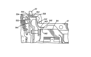
Another spring embodiment 140 is illustrated in
Fig. 7. The spring 140 includes an elongated cantilever 142
having a first end 144 mechanically supported and
electrically connected to the surface of the conductor
terminal 44. This embodiment 140 of the spring illustrates
an alternate site of connection other than the circuit board
80. Preferably, a suitable fastening means like spot
welding is used. Mechanical fasteners like screws and '
rivets are avoided. The support provided by mechanically
securing the first cantilever end 144 and conductor terminal
44 also aligns and positions a second end 146 of the
WO 95/27301 216 3 3 5 9
PCT/US95/03887
-13-
cantilever to make the electrical connection which completes
the test circuit. The second cantilever end 146 makes an
electrical connection on the circuit board 84 with a post
148. The post 148 is electrically connected to the circuit
tracings (not shown) on the circuit board 84. Alternately,
a conductive edge plated solder pad connected to the circuit
board tracings can be used as the electrical terminal on the
circuit board 84 for contacting the second cantilever end
146.
The cantilever 142 includes a first arm 150
located near the first cantilever end 144 and a second arm
152 located near the second end 146 of the cantilever. The
length of the first arm 150 is preferably shaped to conform
to the configuration of the top of the conductor terminal 44
and provide an electrical connection directly with this
terminal of the test circuit.
The second arm 152 abuts the bottom of the test
button 22 and also provides an electrical contact area for
reversibly engaging the rigid conductor 44. Preferably, the
second arm 152 provide a flattened contact area at the
second end 152 for contacting the post 148. The length of
the second arm 152 has the shape of an arch 154 made with a
uniform angle across a portion of the second arm 152. The
arch 154 is integrally formed with the cantilever 142
between the first and second ends 144, 146 and biases the
top of the second arm 152 against the bottom of the test
button 22. The arch 154 exemplifies another flexing means
contemplated by the present invention.
The cross-section of the cantilever 142 has a
flattened, sheet-like shape. A break 156 is provided in the
cantilever to position and align the second cantilever end
146 to contact the circuit board 84.
The spring 140 is made of an electrically
conducting and resilient material. For repeated use, the
spring should be capable of flexing along the arch 154
WO 95/27301 PCT/US95103887
216359
-14-
without cracking or deformation.
As illustrated, the one-piece inventive spring
provides a direct electrical connection between two
terminals of a circuit interrupter test circuit. One of the
unique features is to mechanically support the inventive
spring directly on a terminal of the test circuit such as
the circuit board or the rigid conductor. The use of wire
leads or connectors is eliminated. Assembly of the circuit
interrupter is made easier and inventory costs are lowered
with fewer parts needed.
The present invention is not limited to the use of
a coil to provide torsional flexing for the inventive spring
and the biasing force to reversibly close the terminals of
the test circuit. An angular bend in the body of the spring
is also suitable. Another example of the flexing means is
an arch in a portion of the spring with a uniform or non-
uniform radius.
The inventive spring was tested to prevent
conductance during high voltage surges. This impulse
dielectric test assures that there is ample clearance
between the spring and the terminal of the test circuit to
prevent arcing. The present invention withstood at least a
7 kV pulse test without an arcing failure.
As those skilled in the art will appreciate, the
inventive spring can be adapted and configured for use with
a wide variety of circuit breakers and other circuit
interrupters. The inventive spring is suitable for use in
low, medium, and high voltage applications and in various
phase configurations. The term circuit interrupter is
defined to include but not be limited to, single or
polyphase circuit breakers, vacuum or air circuit breakers,
fusible switches, switchgear, and the like.
The conducting spring methodology and apparatus
described above can be advantageously used for test circuits
in all types of GFCIs and ground fault equipment. Three
WO 95/27301 216 3 3 5 9 pCT~s95/03887
-15-
types of GFCI are commonly available. The first or
separately enclosed type is available for 120-volt 2-wire
and 120/240-volt 3-wire circuits up to 30 amp. The second
type combines a 15-, 20-, 25-, or 30-amp circuit breaker and
a GFCI in the same plastic case. It is installed in place
of an ordinary breaker in a panelboard and is usually
available in 120-volt 2-wire, or 120/240-volt 3-wire types
which may also be used to protect a 2-wire 240-volt circuit.
The second type provides protection against ground faults
and overloads for all outlets on the circuit. A third type
having a receptacle and a GFCI in the same housing provides
only ground-fault protection to the equipment plugged into
that receptacle. There are feed-through types of GFCI which
provide protection to equipment plugged into other ordinary
receptacles installed downstream on the same circuit.
Examples of ground fault equipment are
commercially available from the Square D Company under the
catalog designations GROUND-CENSOR, HOMELINER, QOR,
TRILLIANTR and MICROLOGICR ground fault modules. This
ground fault equipment is suitable for protection of main,
feeder, and motor circuits on electrical distribution
systems. It is also useable as ground fault relay and
ground fault sensing devices.
While particular embodiments and applications of
the present invention have been illustrated and described,
it is to be understood that the invention is not limited to
the precise construction and compositions disclosed herein
and that various modifications, changes, and variations
which will be apparent to those skilled in the art may be
made in the arrangement, operation, and details of
construction of the invention disclosed herein without
departing from the spirit and scope of the invention as
defined in the appended claims.