Note: Descriptions are shown in the official language in which they were submitted.
2~4~ 34
-
OPTICAL PHASE-MODULATING DEVICES
AND METHODS FOR T~EIR OPERATION
Field of the Invention
This invention relates to optical phase-modulating
devices and to methods for their operation. It is
particularly relevant to semiconductor-based integrated
optic devices, including Mach-zehnder interferometers.
Background of the Invention
A known semiconductor-based optical phase-
modulating device comprises a plurality of semiconductor
layers defining an optical waveguide section, and a pair of
phase-modulating electrodes on opposite sides of the
waveguide section. A time-varying electric signal is
applied to the phase-modulating electrodes to apply an
electric field across the waveguide section. The electric ~
field modulates refractive indices of the semiconductor
layers, thereby modulating the effective optical path
length through the waveguide section and the resulting
phase of the optical signal at an output end of the
waveguide section.
Such known optical phase-modulating devices can be
used in the construction of integrated optic devices. For
example, an integrated Mach-Zehnder interferometer can be
constructed from two such optical phase-modulating devices
connected between a waveguide splitter and a waveguide
combiner (Rolland et al, Electronics Letters, Vol. 29, ~o.
5, pp. 471-472, March 4, 1993).
The semiconductor layers which define the optical
waveguide section have a finite resistance. ~onsequently,
electric signals applied to the phase-modulating electrodes
spread along the semiconductor layers beyond ends of the
phase-modulating electrodes. The distributed resistance
and capacitance of the semiconductor layers act as a
~F~E~ SHEEr
~l ~4134
distributed RC network, so that the phase-modulation
provided by the phase-modulation device has an undesirable
frequency dependence. In Mach-Zehnder interferometers
constructed from such phase-modulating devices, the
frequency dependence of phase-modulation results in
frequency dependence of the modulation depth of the
recombined signal.
Summary of the Invention
0 This invention provides semiconductor-based
optical phase-modulating devices and methods for operating
semiconductor-based optical phase-modulating devices which
permit more accurate control of optical phase shifts and
resulting interference signals.
One aspect of the invention provides an optical
phase-modulating device. The device comprises a plurality
of semiconductor layers defining an optical waveguide
section. First and second pairs of electrodes are disposed
on opposite sides of first and second parts of the optical
waveguide section respectively. Constant electric
potential applying means are connected to the first and
second pairs of electrodes to apply constant electric
fields across the first and second parts of the optical
waveguide section, thereby fixing effective optical path
lengths through the first and second parts of the optical
waveguide section. The first and second parts of the
optical waveguide section are longitudinally spaced along
the optical waveguide section. A third pair of electrodes
is disposed on opposite sides of a third part of the
optical waveguide section. The third part of the optical
waveguide section is disposed between the first and second
parts of the optical waveguide section. Variable electric
potential applying means are connected to the third pair of
electrodes for applying a variable electric field across
the third part of the optical waveguide section to vary an
~htE~ûEa S~lEEI
-2154i3~
effective optical path length through the third part of the
optical waveguide section.
The fixation of electric fields across the first
and second parts of the waveguide section by the
phase-fixing electrodes limits the spread of the variable
electric field along the semiconductor layers to reduce the
distributed resistance and capacitance of the
phase-modulating device thereby providing better high
o frequency response. The phase-fixing electrodes also
permit DC biasing of the phase shift provided by the
phase-modulating device.
Preferably, at least one electrode of each of the
first and second pairs of electrodes is spaced from a
respective end of a corresponding electrode of the third
pair of electrodes by a distance which is much shorter than
the corresponding electrode of the third pair of
electrodes.
- 20
The semiconductor layers defining the optical
waveguide section may comprise a pair of cladding layers
having a cladding refractive index and a core layer having
a core refractive index, the core layer being disposed
between the cladding layers and the core refractive index
being greater than the cladding refractive index over a
range of applied electric fields. The cladding layers may
be doped with impurities of opposite conductivity types to
define a doping junction which can be reverse-biased to
apply relatively large electric fields across the waveguide
section.
The optical phase-modulating device is
particularly useful for constructing integrated optical
devices, such as Mach-Zehnder interferometers used for
optical slgnal modulation.
~I~N~EO S~ET
2~ ~134
Thus, another aspect of the invention provides an
integrated optical device comprising an optical waveguide
splitter, first and second optical waveguide devices
coupled to first and second outputs of the optical
waveguide splitter respectively, and an optical waveguide
combiner, coupled to outputs of the first and second
optical modulating devices to produce an optical
interference signal. At least one of the first and second
optical waveguide devices is an optical phase-modulating
o device as defined above.
Another aspect of the invention provides a method
for operating an optical phase-modulating device which
comprises a plurality of semiconductor layers defining an
optical waveguide section. The method comprises applying
constant electric fields across first and second parts of
the optical waveguide section to fix effective optical path
lengths through the first and second parts of the optical
waveguide section while varying an electric field across a
third part of the optical waveguide section to vary an
effective optical path length through the third part of the
optical waveguide section. The first and second parts of
the optical waveguide section are longitudinally spaced
along the optical waveguide section, and the third part of
25- the optical waveguide section is disposed between the first
and second parts of the optical waveguide section.
Convenien~ly, a constant electric potential may
be applied between each of first and second pairs of
electrodes disposed on opposite sides of the first and
second parts of the optical waveguide section respectively
to fix the electric fields across the first and second
parts of the optical waveguide section. A time-varying
electric potential may be applied between a third pair of
electrodes disposed on opposite sides of the third part of
the optical waveguide section to vary the electric field
across the third part of the optical waveguide section.
~U~NDE~ SHEE~
2 ~ 6 ~ 1 3 ~ PCT/CA94/00260
and second parts of the optical waveguide section. A time-
varying electric potential may be applied between a pair of
phase-modulating electrodes disposed on opposite sides of
the third part of the optical waveguide section to vary the
, 5 electric field across the third part of the optical
waveguide section.
The constant electric potential applied between
each of the first and second pairs of phase-fixing
lo electrodes may be a zero potential or may be a non-zero
potential for adjusting a DC phase-bias of the waveguide
section.
srief ne~cr;Dt;on of the DrAwinas
Embodiments of the invention are described below
by way of example only. Reference is made to accompanying
drawings, in which:
Figure 1 is a perspective view of a known
semiconductor-based optical phase-modulating device;
Figure 2 is a cross-sectional view of the phase-
modulating device of Figure 1 taken on section line 2-2 of
Figure 1;
Figure 3 is a schematic diagram of a circuit which
2s models electrical characteristics of the phase-modulating
device of Figure 1;
Figure 4 is a perspective view of a semiconductor-
based phase-modulating device according to an embodiment of
the invention;
Figure 5 is a cross-sectional view of the phase-
modulating device of Figure 4 taken on section line 5-5 of
Figure 4;
- Figure 6 is a schematic diagram of a circuit which
models electrical characteristics of the phase-modulating
device of Figure 4; and
WO95/0~5 PCT/CA94/00260
216 113ll
Figure 7 is a top plan view of an integrated optic
Mach-Zehnder interferometer based on a pair of phase-
modulating devices similar to the device shown in Figure 4.
s Description of Embodiments
Figures 1 and 2 show a known form of semiconductor-
based phase-modulating device 100.
The phase-modulating device 100 is formed on a
lo semiconductor substrate 110 and comprises a first
semiconductor cladding layer 122 on the substrate 110, a
semiconductor core layer 124 on the first cladding layer
122, and a second semiconductor cladding layer 126 on the
core layer 124, the core and cladding layers 122, 124, 126
15 together defining a ridge 120 on the substrate 110. The
core and cladding layers 122, 124, 126 are formed of
different semiconductor compositions so that the core layer
124 has a higher refractive index than the cladding layers
122, 126 so that the ridge 120 functions as a horizontal
optical waveguide section. The first cl~ing layer 122
has the same doping polarity as the substrate 110, and the
second cladding layer 126 has an opposite doping polarity
so the three layers 122, 124, 126 of the ridge 120 also
define a vertical doping junction.
A semiconductor contact layer 130 covers the
second cladding layer 126. The contact layer 130 is formed
of a semiconductor which is heavily doped to the same
doping polarity as the second cladding layer 126. A
dielectric layer 140 covers an upper surface 127 of the
first cladding layer 122 on both sides of the ridge
waveguide section 120 and sidewalls 128 of the ridge
waveguide section 120. A metallic layer 150 contacts the
contact layer 130 and defines an upper phase-modulating
electrode of the device 100. A metallic layer 160 on a
bottom surface 114 of the substrate 110 defines a lower
phase-modulating electrode of the device 100.
1 3 4
O95/0~5 PCT/CA94/00260
-
The device 100 is operated by applying a time-
varying electric potential between the upper and lower
phase-modulating electrodes while propagating light along
the ridge waveguide section 120, the polarity of the
electric potential being such as to reverse bias the
vertical doping junction defined by the cladding layers
122, 126 and the core layer 124. The electrodes apply a
time-varying electric field to the semiconductor layers
o 122, 124, 126, thereby modulating refractive indices of the
semiconductor layers 122, 124, 126. Modulation of the
refractive indices modulates the effective optical path
length through the ridge waveguide section 120, thereby
modulating the phase at an output end of the ridge
waveguide section 120 of light propagated through the ridge
waveguide section 120.
The semiconductor layers 110, 122, 124, 126, 130
have a finite resistance. Consequently, electric signals
applied to the phase-modulating electrodes spread along the
semiconductor layers 110, 122, 124, 126, 130 beyond ends of
the phase-modulating electrodes. The distributed
resistance and capacitance of the semiconductor layers 110,
122, 124, 126, 130 can be modelled as a distributed RC
network 180 as shown in Figure 3, where C is the
capacitance of the layers 110, 122, 124, 126, 130 under the
upper phase-modulating electrode 150, and r and c are the
resistance and capacitance per unit length of the layers
110, 122, 124, 126, 130 beyond ends of the upper phase-
modulating electrode 150. The distributed resistances r
and capacitances c define a low pass filter, so that the
phase-modulation provided by the phase-modulation device
- 100 has an undesirable frequency dependence.
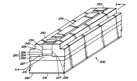
- 35 Figures 4 and 5 show a semiconductor-based phase- modulating device 200 according to an embodiment of the
W095/0~ 216 41 3 ll PCT/CA94/00260
invention. This phase-modulating device 200 is formed on
an n-type InP substrate 210.
The phase-modulating device 200 comprises an n-
type InP cladding layer 222, an intrinsic Multiple QuantumWell (MQW) core layer 224 on the n-type cladding layer 222,
and a p-type InP cladding layer 226 on the core layer 224.
The MQW core layer 224 has a higher refractive index than
the InP cladding layers 222, 226, so that the core and
o cladding layers 222, 224, 226 together define a ridge which
acts as a horizontal optical waveguide section 220. The
core and cl~;ng layers 222, 224, 226 also define a
vertical pin doping junction.
The phase-modulating device 200 further comprises
a contact layer 230 of p-type InGaAs which covers the p-
type cladding layer 226 and a dielectric layer 240 of
silicon dioxide which covers an upper surface 227 of the
lower cladding layer 222 on both sides of the ridge
waveguide section 220 and sidewalls 228 of the ridge
waveguide section 220.
The phase-modulating device 200 has three TiPtAu
upper metallic layers 2S0, 252, 254 spaced along the ridge
waveguide section 220, each contacting the contact layer
230. First and second upper metallic layers 250, 252 are
20 microns long and are spaced from opposite ends of the
third upper metallic layer 254 by 20 microns, the third
upper metallic layer 254 being 600 microns long.
The phase-modulating device 200 further
comprises a Ni/Ge/Au/Ti/TiN/Au lower metallic layer 260 on
a bottom surface 212 of the substrate 210.
The distinct upper metallic layers 250, 252, 254
define three longitudinally-spaced series-connected parts
270, 272, 274 of the waveguide section 220, each part 270,
~95/0~5 ~ 1 ~ 41 ~ ~ PCT/CA94/00260
272, 274 underlying a respective metallic layer 250, 252,
254. The first and second upper metallic layers 250, 252
define upper phase-fixing electrodes while the third upper
metallic layer 254 defines an upper phase-modulating
electrode. Regions of the lower metallic layer 260 beneath
the first and second waveguide sections 270, 272
respectively define first and second lower phase-fixing
electrodes while a region of the lower metallic layer 260
beneath the third waveguide section defines a lower phase-
o modulating electrode.
The phase-modulating device 200 is operated by
applying a time-varying electric potential between the
upper and lower phase-modulating electrodes while
lS propagating light along the waveguide section 220, the
polarity of the electric potential being such as to reverse
bias the pin doping junction defined by the core and
cl~ding layers 222, 224, 226. The phase-modulating
electrodes apply a time-varying electric field across the
third part of the waveguide section 220, thereby modulating
refractive indices of the semiconductor layers 222, 224,
226 in the third part of the waveguide section. Modulation
of the refractive indices modulates the effective optical
path length through the third part of the waveguide section
220.
At the same time, a constant electric potential is
applied between each upper phase-fixing electrode and its
corresponding lower phase-fixing electrode to fix the
electric field across the first and second parts of the
waveguide section 220. This effectively limits the spread
of the time-varying electric potential along the waveguide
- section 220 to reduce frequency dependent variation of the
phase-modulation provided by the device 200.
In practice, the device 200 is operated by
grounding the lower metallic layer 260 and applying a
W095/0~5 ~ ~ 6 ~ ~ 3 ~ PCT/CA94/00260
constant potential with respect to ground to the first and
second upper metallic layers 250, 252 while applying a time-
varying potential with respect to ground to the third upper
metallic layer 254 while propagating light along the
waveguide section 220.
Usually, the first and second upper metallic
layers 250, 252 are grounded so;that there is a zero
potential between each pair of phase-fixing electrodes. In
this case, the distributed resistance and capacitance of
the semiconductor layers 210, 222, 224, 226, 230 can be
modelled as a distributed RC network 280 as shown in Figure
6. Grounding of the first and second upper metallic layers
250, 252 effectively connects shunts S across significant
portions of the distributed RC network, thereby reducing
undesirable frequency dependence of the phase-modulation
characteristics of the device 200.
In some instances it may be advantageous to apply
a non-zero DC potential between one or both pairs of phase-
fixing electrodes to adjust a DC phase-bias of the
waveguide section 220.
The phase-modulating device 200 can be fabricated
according to conventional semiconductor device fabrication
techniques. For example, the n-type cladding layer 222,
the core layer 224, the p-type cladding layer 226 and the
contact layer 230 are successively epitaxially grown on the
substrate 210 by Organo-Metallic Vapour Phase Epitaxy
(OMVPE), by Molecular Beam Epitaxy (MBE) or by other
suitable epitaxial growth techniques. Typical layer
thicknesses, compositions and dopings are:
T.~yer Thickness Comnosition DoDi nq
cladding 222 2 microns InP n: 5X10l7 cm-3
35MQW core 224 0.4 microns InP/InGaAsP intrinsic
cladding 226 2 microns InP p: 5X10l7 cm-3
contact 230 0.2 microns InGaAs p+: 1019 cm-3
2 1 ~ 4 1 3 ~ PCT/CA941~0260
The MQW core layer 224 comprises 20 sublayers of InP
interleaved with 20 sublayers of InGaAsP, each sublayer
being lO0 Angstroms thick.
- 5 The ridge waveguide section 220 is protected with a photolithographically defined mask, and unprotected
regions of the contact, upper cladding and core layers 230,
226, 224, and approximately 0.3 microns thickness of the
lower cladding layer 222 are removed by dry-etching to
define the waveguide sectlon 220. The waveguide section
220 is typically 2 microns wide.
The conformal silicon dioxide layer 240 is
deposited to a 3 micron thickness by Plasma Enhanced
Chemical Vapour Deposition (PECVD). Photoresist is spun on
to define a substantially planar upper surface, and the
photoresist is etched back to reveal the top of the ridge
waveguide 220. The distinct layers 250, 252, 254 of TiPtAu
are formed and defined using conventional liftoff
techniques. The Ni/Ge/Au/Ti/TiN/Au layer 260 is then
formed on the bottom surface of the substrate by successive
electron beam evaporation deposition of individual metallic
sublayers followed by heating to alloy the metallic layer
260.
The resistivity of the semiconductor layers of
the waveguide section 220 and the spacing between the upper
phase-fixing electrodes and the upper phase-modulating
electrode are selected so as to achieve a desired frequency
response and input impedance for the device 200. The
frequency response of the device 200 can be flattened by
reducing the spacing between the phase-fixing electrodes
- and the phase-modulating electrode. However, reducing the
spacing between the phase-fixing electrodes and the phase-
- 35 modulating electrode also reduces the shunting resistance
between these electrodes. Consequently, there is a design
tradeoff between the flatness of the frequency response and
W095/0~5 PCT/CA94/00260
~16413 l
the shunting resistance. In the device described above,-
the shunting resistance is approximately 3000 ohms, and the
3 ds bandwidth in a 50 ohm system is approximately lS GHz.
s The phase-modulating device 200 can be used as a
basic building block in a variety of integrated optics
applications. For example, the phase modulating device can
be used in the construction of an integrated optic Mach-
Zehnder interferometer 500 as shown in the plan view in
lo Figure 7.
The interferometer 500 comprises an optical
waveguide splitter 510, first and second optical phase-
modulating devices 200, 200~ as described above, and an
optical waveguide combiner 520, all formed on a common
substrate 530. The first and second phase-modulating
devices 200, 200' are coupled to first and second outputs
512, 514 of the waveguide splitter 510 respectively, and
the waveguide combiner 520 has first and second inputs 522,
524 coupled to outputs of the first and second phase-
modulating devices 200, 200~ respectively.
To operate the interferometer, an optical signal
is launched in the waveguide splitter 510, constant
potentials are applied to the phase-fixing electrodes of
the phase-modulating devices 200, 200~ and time-varying
potentials are applied between the phase-modulating
electrodes of the phase-modulating devïces 200, 200'.
The waveguide splitter 510 divides the launched
light into two optical signals. Differences in the time-
varying potentials applied to the first and second phase-
modulating devices 200, 200~ result in different phase
shifts as the two signals pass through the phase-modulating
devices 200, 200'. The phase-shifted optical signals
recombine to produce an interference signal in the
waveguide combiner 520. The intensity of the interference
~1641~
~95/0~5 PCT/CA94/00260
-
signal depends on the difference of the phase shifts
produced by the phase-modulating devices 200, 200'. The
intensity is maximized at zero phase difference and
minimized at a 180 degree phase difference.
Usually, the time-varying potential applied to the
- second phase-modulating device 200' is an inverted version
of the time-varying potential applied to the first phase-
modulating device 200 to m;n;mi ze the AC signal amplitude
0 required to achieve a desired modulation depth of the
interference signal. Usually a zero potential is applied
between all pairs of phase-fixing electrodes of both phase-
modulating devices 200, 200'. However, a non-zero DC
potential could be applied to the phase-fixing electrodes
of one phase-modulating device to produce a DC phase
difference between the two recombined signals.
One of the phase-modulating devices 200, 200' of
the interferometer 500 could be replaced with a plain
waveguide section. In this configuration, all phase-
modulation would be provided by the single r~m~;n;ng phase-
modulating device.
Waveguide splitters suitable for use in the
2s interferometer 500 are described by C. Rolland et al in
IEEE Photonics Technology Letters, Vol. 2, No. 6, June
1990, p.404-406, which is hereby incorporated by reference.
Numerous modifications could be made to the phase-
modulating device 200 without departing from the principlesof the invention.
~ For example, the waveguide section 220 could be a
buried semi-insulating waveguide section rather than a
ridge waveguide section.
WOgS/0~45 21 ~ 4 PCT/CA94/00260
Other semiconductor materials systems could be
used to form the waveguides, and other conductor
compositions could be used to form the electrodes.
s The core layer 224 of the waveguide section 220
could be a single InGaAsP layer instead of a MQW layer
comprising multiple sublayers of alternating compositions.
However, this modification would degrade the high frequency
performance of the device 200.
The lower metallic layer 260 could be divided into
distinct electrode regions to provide increased flexibility
in biasing the phase-modulating device 200.
These and other modifications are within the scope
of the invention as claimed below.