Note: Descriptions are shown in the official language in which they were submitted.
2164247
FIELD OF THE INVENTION
This invention relates to the field of
telephony, and in particular to a ringing signal
discriminator.
BACKGROUND TO THE INVENTION
Ringing signal discriminators (referred to
below as ring discriminators) detect the presence of
ringing signals from other signals that may be present
on a telephone line, such as noise, dual tone
multifrequency (DTMF) signals, crosstalk from other
telephone lines, control signals of various types,
harmonics generated from various signals and noise such
as control signals, etc.
In certain jurisdictions a ringing detector is
required to react to any signal of at least a certain
amplitude within the frequency band of 23 and 54 Hz as a
true ringing signal, and outside of the band of 18 and
64 Hz as a false signal. 18-24 and 45-64 Hz zones are
insensitive zones (see Figure 1). Frequencies 20 and 60
Hz are chosen roughly in the middle of the insensitive
zones as two digital thresholds between which the
existence of a ringing signal is considered to be true.
The reason for that is that the factor 3 (60/20) is easy
to detect digitally.
A ringing signal is thus considered to have a
frequency of between 20 Hz and 60 Hz. Only +/- 8.3%
separates 64 Hz, a false ringing frequency threshold,
and 54 Hz, which is within the band and which is a true
ringing frequency threshold. It has been found that
circuits that use analog signals are slow in detecting
the ringing signal, requiring several ringing cycles to
be able to detect the ringing signal, and are sensitive
to tolerance variations in the components which make up
the ringing signal.
216~2~7
Slow ringing signal detection can result in
lost calls due to a receiving party taking a handset off
hook prior to completion of ringing signal detection.
Ringing signals cannot be recognized in this case though
they exist, and connection of the call cannot be made.
Sensitivity to tolerance variations can result in in-
band ringing signals not being detected or out-of-band
signals being mistaken for in-band ringing signals.
SUMMARY OF THE INVENTION
The present invention is a ring discriminator
which can detect the presence of a ringing signal at the
end of only one and a half of a first ringing cycle, and
thus can provide a ringing control signal extremely
quickly to a called party or to equipment which is
enabled in the presence of a ringing signal. Further,
the sensitivity of the present invention to component
tolerance variations is substantially reduced due to a
ringing signal detection mechanism which is for the most
part digital.
In accordance with the present invention, a
ring discriminator is comprised of apparatus for
receiving an input ringing signal, a counter, apparatus
for applying clock pulses to the counter, apparatus for
enabling the counter to count clock pulses from a cycle
of ringing current, and apparatus for determining a
clock pulse count on the counter to distinguish a
frequency characteristic of the ringing signal. It is
preferred that the cycle of ringing current is a first
cycle in a ring burst.
In accordance with a further embodiment, in the
aforenoted ring discriminator the counter enabling
apparatus is comprised of apparatus for detecting the
beginning and the end of a single pulse period for
generating an enable pulse beginning and ending at the
2164247
beginning and end of the single pulse period, and for
applying the enable pulse to the counter.
BRIEF INTRODUCTION TO THE DRAWINGS
A better understanding of the invention will be
obtained by reading the description of the invention
below, with reference to the following drawings, in
which:
Figure 1 is a frequency chart of in-band and
out-of-band ringing signals,
Figure 2 is a schematic diagram of a preferred
embodiment of the present invention, and
Figure 3 is a waveform diagram illustrating the
forms of signals at various locations in the circuit
illustrated in Figure 1.
DETAILED DESCRIPTION OF THE INVENTION
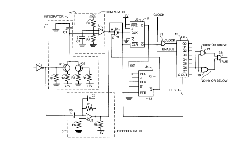
A preferred embodiment of the invention will be
described with reference to both of Figures 2 and 3
together. A ringing signal to be discriminated, shown as
the RING IN signal in Figure 1, is applied to the input
of an operational amplifier 1, which acts to both buffer
the ringing signal and to limit it (e.g. by clipping)
into somewhat square-wave form.
The output signal of clipping operational
amplifier 1 is applied to the inputs of a differentiator
3, which differentiates the leading edge of the output
signal from operational amplifier 1. That
differentiated signal is shown as the DIFF OUT signal in
Figure 3.
The output signal of operational amplifier 1 is
also applied to the input of an integrator 5, which has
a fast charge time and a slow discharge time. The
integrated output signal may be detected across
capacitor C1, and is shown in Figure 3 as signal CAP C1.
Both the integrator and differentiator are of
conventional and well known construction.
CA 02164247 1999-03-10
The output signal of the integrator S is
applied to one input of a comparator 7, which converts
the output of the integrator into square wave. Since
the integrator integrates the ringing signals over all
cycles of each ring burst, the square wave output signal
from integrator S is a pulse which lasts the interval of
the ring burst (i.e. corresponds to the ring burst
envelope), but starts later than the beginning of the
first ringing cycle by a phase shift of 90 degrees.
This will occur at whatever the frequency of the ringing
signal.
Both the output signal of the comparator 7 and
the output signal of the differentiator 3 are applied to
respective inputs of NAND gate 9. The output of the
NAND gate 9 is applied to the clock input CLK of a first
self-latching flip flop 11. The Q output of flip flop
11 is applied to the clock input CLK of a second self-
latching flip flop 13, and the /Q output of flip flop 13
is connected to another input of NAND gate 9. An enable
pulse is provided at the /Q output of flip flop ll, as
will be described below.
Prior to the receipt of an input ringing
signal, the /Q output of flip flop 13 is at high logic
level, as may be seen from waveform U4 in Figure 3, and
is applied to an input of NAND gate 9. With the receipt
of ringing signals, the output of the comparator 7
(signal U1 OUT in Figure 3) goes to high logic level,
with the envelope of the ringing burst, and is received
at an input to NAND gate 9. Pulses resulting from
differentiation of the leading edges of the ringing
cycles as indicated by the DIFF OUT signal are applied
to an input of NAND gate 9. The result are pulses at
the output of NAND gate 9 of the waveform U5 OUT shown
in Figure 3. Those pulses are received at the CLK input
of flip flop 11.
,
CA 02164247 1999-03-10
With the receipt of the first pulse at the CLK
input of flip flop 11, its /Q output goes to high logic
level, shown as waveform U3 /Q OUT, and its Q output
goes to low logic level. With the receipt of the second
pulse at the CLK input of flip flop 11, its /Q output
goes to low logic level and its Q output goes to high
logic level, as may be seen in Figure 3. Thus for the
interval of one ringing cycle the output /Q is at high
logic level, and outside that ringing cycle that output
is at low logic level.
The inverse of that pulse, at the Q output of
flip flop 11, is applied as a clock pulse to the CLK
input of flip flop 13. As a result, the /Q output of
flip flop 13 changes from high to low logic level at the
termination of the clock pulse applied to its CLK input.
That low logic level signal, applied to an input of NAND
gate 9, causes inhibition of the differentiated leading
edges of the ringing signal from passing through NAND
gate 9. As a result only two of such pulses pass
through NAND gate 9, representing the beginning of
successive ringing cycles, i.e. the beginning and the
end of a single ringing cycle (shifted 180 degrees) and
being the first ringing cycle of a ring burst. This may
be seen from the waveform diagrams of Figure 3.
Thus only a single pulse signal /Q OUTPUT is
provided at the /Q output of flip flop 11 resulting from
the first ringing cycle of a ring burst. That single
pulse signal is used as an enable signal to an enable
input of a binary counter 15.
A clock signal is also applied to the counter
15, preferably through an AND gate 17 with the enable
pulse, as shown.
Thus during the interval of an enable pulse,
clock signals can pass through AND gate 17 to the
counter 15, which is enabled to count clock pulses
21642~7
during that interval. The count reached by the counter
represents the period of the enable pulse, which
corresponds directly to the frequency of the input
ringing signal.
To discriminate the frequency of a received
ringing signal as being within or outside a standard
ringing frequency band, the Q6 and Q7 terminals of the
counter are connected to the respective inputs of a NOR
gate 19 and to the respective inputs of a NAND gate 21.
The outputs of gates 19 and 21 are applied to the inputs
of an AND gate 23. The output of AND gate 23 is an
output signal which indicates by a TRUE signal if the
input ringing signal frequency is within a band
indicated by the clock count reached by counter 15
during the interval when it is enabled.
To reset the circuit, the Ul OUTPUT signal,
which lasts for the interval of the ring burst envelope,
from the output of comparator 7, is applied to the clear
inputs CLR of both flip flops 11 and 13, and to the
reset input RESET of the counter 15. Thus when the Ul
OUTPUT signal goes to low logic level, at the end of a
ring burst, both flip flops are reset to their initial
state and the counter is cleared, ready for receipt of a
subsequent ring burst.
As an example in the diagram illustrated if the
count reaches 01000000 (decimal 64) the frequency of the
input ringing signal is 60 Hz and if the count reaches
11000000 (decimal 192) the frequency of the input
ringing signal is 20 Hz. These frequencies represent
the highest and lowest threshold frequencies of the
ringing signal band. The clock frequency, the clock
pulses of which are counted by the counter 15, in this
case can be calculated as 64 (count) x 60 (Hz) = 3840
Hz, or 192 (count) x 20 Hz = 3840 Hz.
216~2~7
It will of course be recognized that the number
of bits counted in the counter 15 may be used, a
different counter may be used, and various forms of
logical circuits may be used to realize the present
invention, other than the exact circuitry shown, to
realize the present invention. In addition the present
invention can be used to discriminate signals other than
ringing signals, and the term ringing signals should be
construed to mean any input signals of similar
characteristic which are capable of being discriminated
by the present invention. In addition the circuitry
connected to the output of the counter 15 may be used to
indicate the frequency or period of the ringing input
signal, rather than merely that the ringing input signal
is within a particular band of frequencies.
A person understanding this invention may now
conceive of alternative structures and embodiments or
variations of the above. All of those which fall within
the scope of the claims appended hereto are considered
to be part of the present invention.