Note: Descriptions are shown in the official language in which they were submitted.
~ 2164465
-- 1 --
C~.V~ FOR CO`NV~1NG A MODULATING SIGNAL WITH U~pT~RT.~.
ENVELOPE TO TWO MODULATING SIGNALS WITHOUT VpRT~RT-~
ENVELOPE,
T~S~I'1L~K USING THE CO1.V~KTER
AND
METHOD FOR TRANSMITTING A MODULATED WAVE WITH VApT~RT-~
ENVELOPE
R~K~OUND OF THE lNv~LlON
o The present invention relates to an art for transmitting
a modulated wave with variable envelope, such as 4-phase
Phase Shift Keying (hereinafter referred to as PSK), ~/4
shift Differential Quadrature Phase Shift Keying
(hereinafter referred to as DQPSK) and the like.
A conventional digital cellular phone system employs a
linear modulation method using a modulated wave with a
narrow band width such as ~/4 shift DQPSK for efficient
use of frequency. However this linear modulation method
varies the amplitude of transmission radio wave to a great
degree compared to the conventional constant envelope
modulation method (where the envelope does not vary)
employing Frequency Modulation (hereinafter referred to as
FM), Gaussian Minimum Shift Keying (hereinafter referred to
as GMSK) modulation and the like. As a result, a
transmitter is required to transmit the above-described
~_ 21 64465
-- 2 --
amplitude variation accurately. That is why a linear
amplifier has to be used in spite of its
ineffectiveness.
Fig. 3 shows a block diagram of a conventional
transmitter.
A base band waveform generation circuit 1 receives an
incoming input data signal 7, synchronizing with a clock
8 and outputs corresponding base band signals
(modulating signal) I and Q, respectively. The signal I
lo refers to an in-phase component of the transmisslonradio wave to the carrier. The signal Q refers to a
quadrature component.
These signals are input to an quadrature modulator 2
for quadrature modulating a local signal (carrier)
output from a local oscillator 6. Output signals
(modulated signal) of the quadrature modulator 2 are
amplified with a transmission power amplifier 3 and
transmitted from an antenna 5 after eliminated
unnecessary waves through a transmission filter 4.
The output of the quadrature modulator 2 as linear
modulation such as ~/4 shift DQPSK, QPSK and the like,
is accompanied with the envelope amplitude variation
because of using no constant envelope modulation. The
transmission power amplifier 3 has to be a linear
2s amplifier in order to reproduce the envelope amplitude
21 64465
- 3
variation as accurate as possible.
Fig. 4 is a graphlcal representation of
- characteristics of a transmission power amplifier. An
axis of abscissa is an input level, a left axis of
ordinates is an output level and a right axis of
ordinates is efficiency. The solid line designates a
relationship between input power and output power. The
dotted line designates a relationship between the input
power and efficiency.
The conventional transmission method has no chance but
uses the area where the output power linearly varles to
the input power in order to conduct linear
amplification. This area, however, exhibits quite low
efficiency. Moreover the conventional method increases
power consumption for transmission compared with the
constant envelope modulation method applicable in the
non-linear area (lower right section of the graph of
Fig. 4).
The above described conventional method for amplifying
the linear modulated wave with the linear amplifier
exhibits quite low power efficiency, resulting in
excessive power consumption increase.
SUMM~RY OF THE l~v~NL-lON
It is an object of the invention to provide a solution
for the aforementioned problem.
~_ 21 64465
-- 4
Another object of the invention is to provide a
transmitter and a method enabling to use a non-linear
and efficient amplifier for transmission power
amplification.
The aforementioned present invention is achieved by a
converter for converting a modulating signal with
envelope variation to two modulating signals without
envelope variation, the converter comprising means for
converting a signal of the modulating signal with
o envelope variation of which in-phase component signal is
I and quadrature component signal is Q to a signal of
which in-phase component signal is I1, and quadrature
component signal is Q1 and a signal of which in-phase
component signal is I2, and quadrature component signal
is Q2 that meet the following conditions (1) to (3):
(I1)2 + (Q1)2 = constant (1)
(I2)2 + (Q2)2 = constànt (2)
Vector (I,Q) = Vector (I1,Q1) + Vector (I2,Q2) (3).
Moreover, the aforementioned present invention is
achieved by a transmitter comprising:
means for converting a signal of the modulating signal
with envelope variation of which in-phase
component signal is I and quadrature component
signal is Q to a signal (of which in-phase
component signal is I1, and quadrature component
. ~ 2164465
-- 5
signal ls Ql) and a signal (of which in-phase
component signal is I2, and quadrature component
signal is Q2) that meet the following conditions
(1) to (3):
S (Il)2 + (Ql)2 = constant (1)
(I2)2 + (Q2)2 = constant (2)
Vector (I,Q) = Vector (Il,Ql) + Vector (I2,Q2) (3),
a first modulation means for modulating a carrier with
the signal (Il,Ql) and generating a first modulated
o wave;
a second modulation means for modulating a carrier
with the signal (I2,Q2) and generating a second
modulated wave;
a first amplification means for power amplifying the
lS first modulated wave;
a second amplification means for power amplifying the
second modulated wave; and
means for composing outputs signals of the first
amplification means and the second amplification
means.
Furthermore, the aforementioned present invention is
achieved by a method for transmitting a modulated wave
with envelope variation, the method comprising steps of:
converting a signal of the modulating signal with
envelope variation of which in-phase component
-- 6 --
signal ls I and quadrature component signal is Q
to a signal of which in-phase component signal is
Il, and quadrature component signal is Ql and a
signal of which in-phase component signal is I2,
and quadrature çomponent signal is Q2 that meet
the following conditions (1) to (3):
(Il)2 + (Ql)2 = constant (1)
(I2)2 + (Q2)2 = constant (2)
Vector (I,Q) = Vector (Il,Ql) + Vector (I2,Q2) (3);
a first modulation step of modulating a carrier with
the signal (Il,Ql) and generating a first modulated
wavei
a second modulation step of modulating a carrier with
the signal (I2,Q2) and generating a second
S modulated wave;
a first amplification step of power amplifying the first
modulated wave;
a second amplification step of power amplifying the
second modulated wave;
composing the first power amplified modulated wave and
the second power amplified modulated wave;
band limiting a composed modulated wave; and
transmitting a band limited modulated wave.
The present invention converts a modulating signal of
which amplitude is variable (i.e., of which envelope is
- ~ 21 64465
7 --
variable) to two constant envelope modulating signals.
Then the present invention modulates, amplifies and
composes respective carriers by using respective
constant envelope modulating signals. Thus, the present
invention allows to use a non-linear and highly
efficient amplifier, resulting decreasing of power
consumptlon.
BRIEF DESCRIPTION OF T B DRAWINGS
This and other objects, features and advantages of the
present invention will become more apparent upon a
reading of the following detailed description and
drawings, in which:
Fig. 1 is a figure for explaining a principle of the
present invention;
Fig. 2 is a block diagram of an embodiment of the
present invention;
Fig. 3 is a block diagram of a conventional
transmitter; and
Fig. 4 is a figure showing characteristics of a
transmission power amplifier.
DESCRIPTION OF TB PREFERRED EMBODIMENTS
A principle of the present invention is hereinafter
described.
Fig. 1 is a vector representation of phase and
2s amplitude of a signal.
~_: 21 64465
8 --
Assuming that a vector of a transmission modulating
signal is designated as A, in-phase component to the
carrier is designated as I and quadrature component is
designated as Q, the vector A is expressed as the
following coordinate:
A = (I, Q) ... (1)
Assuming that an amplitude "a" of the vector A is
variable, each vector of Al and A2 is supposed to have a
constant amplitude with its value equal to or more than
o 1/2 of the maximum value of the amplitude "a". It is
assumed that A1 and A2 have the same amplitude values of
1 for simplification ~i.e., a < 2). The vectors Al and
A2 are expressed as the following coordinates:
Al = (Il, Ql), A2 = (I2, Q2)
The values of Il, Q1l I2 and Q2 are selected so that the
sum of the vectors Al and A2 is equal to the vector A.
Each of the above value is obtained by the following
equations of (3-1) to (3-4).
Il = {I+Q SQRT(4/a2 - 1)}/2 .... (3-1)
Q1 = {Q-I SQRT(4/a2 - 1)}/2 .... (3-2)
I2 = {I-Q SQRT(4/a2 - 1)}/2 .... (3-3)
Q2 = {Q+I SQRT(4/a2 - 1)}/2 .... (3-4)
where SQRT(x) refers to a square root of the x. The
above equations (3-1) to (3-4) obviously show that:
2s I12 + Q12 = 1 and I22 + Q22 = 1. This represents that
2 1 64465
~, .
signals (Il,Ql) and (I2,Q2) are constant envelope
modulating signals, respectively.
This also shows that:(Il,Ql) + (I2~Q2) = (I~ Q)
As aforementioned, it is possible to obtain an
envelope modulating signal with variable phase component
(I, Q) by generating the constant envelope modulating
signal with the phase component of (Il,Ql) and the the
same valued constant envelope modulated wave with the
phase component of (I2,Q2) and amplifying and composing
0 them with the same gain.
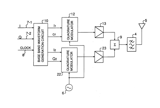
A transmitter of the present lnvention is described
referring to Fig. 2.
As shown in Fig. 2, the transmitter of the present
invention comprises a base band waveform generation
circuit (converter) 10 for outputting base band signals
(modulating signals) Il, Ql, I2 and Q2 based on an in-
phase component signal I, quadrature component signal
(modulating signal) Q and a clock 8 synchronized with
input data; a first quadrature modulator 12 for
quadrature modulating a local signal (carrier) output
from a local oscillator 6 by using the in-phase
component signal Il and the quadrature component signal
Ql; a second quadrature modulator 22 for quadrature
modulating a local signal (carrier) by using the in-
2s phase component signal I2 and the quadrature component
~ 21 64465
- 10 -
signal Q2i a first transmission power amplifier 13 for
amplifying the output signal of the first quadrature
modulator 12, a second transmission power amplifier 23
for amplifying the output signal output from the second
S quadrature modulator 22, a power composition device 9
for composing output signals of the transmission power
amplifiers 13 and 14; a band pass filter 4 for band
limiting the output signal of the power composition
device 9 and an antenna 5 for transmitting the output
signal of the band pass filter 4.
The base band waveform generation circuit 10 (the
converter) applies equations (3-1) to (3-4) to the input
data 7, supplies the in-phase component signal I1 and
the quadrature component signal Q1 to the first
quadrature modulator 12 and supplies the in-phase
component signal I2 and the quadrature component signal
Q2 to the second quadrature modulator 22.
Where, the base band waveform generation circuit 10
comprises a digital signal processor in which a software
for calculating equations (3-1) to (3-4) is embedded.
The first quadrature modulator 12 quadrature modulates
the local signaI (carrier) output from the local
oscillator 6 with the in-phase component signal I1 and
the quadrature component signal Q1.
2s The second quadrature modulator 22 quadrature
2 1 64465
-- 11 --
modulates the local signal (carrier) with the in-phase
component signal I2 and ~he quadrature component signal
Q2-
Output signals of the first quadrature modulator 12
S and the second quadrature modulator 22 are poweramplified through the first transmission power amplifier
13 and the second transmission power amplifier 23,
respectively. Since the output signals of the first and
the second quadrature modulators 12 and 22 are constant
lo envelope modulated waves processed through the base band
waveform generation circuit 10 as aforementioned, no
distortion occurs in spite of power amplification with
the non-linear and highly efficient power amplifier.
The output signals of the first and the second-
transmission power amplifiers 13 and 23 are powercomposed through the power composition device 9. As a
result, with the output signal of the power composition
device 9, the local signal (carrier) is quadrature
modulated with the in-phase component signal I and the
quadrature component signal, thus providing the signal
comparable to that of power amplified with no
distortion.
The output signal of the power composition device 9 is
supplied to the antenna 5 for transmission, after band
limited with the band pass filter 4.