Note: Descriptions are shown in the official language in which they were submitted.
Wo 94~0028 PCTnUS94/06717
2t 65424
MULTI PROTOCOL PERSONAL COMMUNICATIONS SYSTEM
s
CRO8S-REFERENCE
The present application is related to the
following pPn~ing patent application by the same inventor:
10"DIGITAL TELEPHONE, ~RT-~ TV SYSTEM AND LOCAL
EXCHANGE BYPASS NETWORK", Serial No. 07/761,281 Filed
September 17, 1991.
"METHOD AND APPARATUS FOR ~RTNG OF COMMON IN-
HOUSE WIRING TO PERMIT MULTIPLE TELEPHONE CARRIERS TO
15SERVE THE SAME CUSTOMER", Serial No. 07/949,424 Filed
September Z2, 1992.
"CELL BASED WIDE AREA NETWORK ALTERNATIVE ACCESS
TELEPHONE AND DATA SYSTEM", Serial No. 07/953,744
Filed September 29, 1992.
20"WIDE AREA FIBER AND TV ~pRT-~ FAST PACKET CELL
NETWORK", Serial No. 08/000,373 Filed January 4, 1993.
BACRGROUND OF THE INVENTION
1. Field of the Invention
This invention relates to personal communication
networks in general and, in specific, those that use a TV
cable system as a transmission medium and where signals are
sent using ATM compliant cell formats.
2. De~cri~tion of Related Art
A significant portion of a long distance
telephone bill is attributable to transfer payments
required to be made by the long distance carrier to the
local telephone companies at each end of the circuit. To
w~s41so~8 PCT~S94/~717
21 65424
reduce such fees for local interconnection, long distance
inter-exchange carriers seek an alternative path to deliver
signals from a subscriber's telephone directly to the long
distance carrier switch thus bypassing local telephone
companies facilities.
In the co-pending patent applications identified
above in the Cross Reference section, ATM based
communications systems are described wherein cordless
terminal devices generate and utilize ATM compliant fast
packet cells transmitted over TV cable and/or fiber optic
pathways. In the cross-referenced patent applications cell
based formats are used throughout. Starting at the user's
terminal device, the cells are transmitted using cordless
means, and thence over cable and fiber optic paths to reach
area wide ATM networks for interconnection to the world's
telephone systems.
It would be desirable to have a system that is
consistent with the system described in the earlier cross-
referenced patent applications, but creates an evolutionary
path towards the eventual development of that system
without requiring the full system configuration to be in
place at the outset. The objective is to create an interim
minimal system that can grow into the larger system
containing the Directory Computer and interconnected ATM
network described in the earlier referenced patent
applications.
8UMMARY OF T~E INVENTION
In accordance with the present invention there is
shown a bi-directional transmission system for conveying
data between at least one terminal unit which receive and
transmit data in the same signal format as each other and
a transmission interface unit. The signals to and from the
terminal units are carried by a first communications link
wu ~ PCT~S94/06717
21 65424
to a relay transceiver where the signals from the terminal
units are converted bi-directionally between the signal
format of the terminal units and fixed length compliant ATM
cells when the signal format of the terminal units is other
than a fixed length compliant ATM cell format. Via a
second communications link the bi-directional transfer of
fixed length compliant ATM cells is performed with a
transmission interface unit. In the transmission interface
unit there is a bi-directional conversion of the fixed
length compliant ATM cells to time division multiplexed
signals in the upstream direction and from time division
multiplexed signals to fixed length compliant ATM cells in
the downstream direction, wherein the u~L~eam signal
direction is toward the transmission interface unit and the
downstream signal direction is toward the terminal units.
There is also shown a bi-directional
communications system for bypassing a local exc~n~e
carrier telephone system which is an extension of the bi-
directional transmission system described above with the
time division multiplex signal being ~Y~ ged bi-
directionally via a third communications link between the
transmission interface unit and a switching unit that has
the functionality of a Class 5 central telephone office
switch that is connected to a public switched tel~phonQ
network.
Further, either the bi-direction transmission
system or the bi-directional communication æystem described
above can include a æD~onA communications link that
includes a multiplicity of n bi-directional tandemly
connected second communications links and a third
communications link includes a multiplicity of m bi-
directional tandemly connected third communications links.In such a system the transmission interface unit, for
maximum utility should also have sufficient capacity to
U~ PCT/US94/U6717
21 65424
convert signals from any of the n second communications
links to any of the m third communications links, wherein
n and m are each positive integers.
In yet another embodiment of the present
invention in either of the systems discussed above there
can be at least two terminal units each designed to
transmit and receive in different signal formats from each
other and a programmable relay transceiver unit. In this
embodiment the relay transceiver unit includes a software
definable transmitter, a software definable transmitter, a
receiver processing unit and a transmitter processing unit.
The function of the software definable transmitter unit is
to transmit radio signals via the first communications link
to one of the terminal units in the signal format of that
terminal unit. The function of the software definable
receiver unit is to receive radio signals also via the
first communications link from one of the terminal units.
To control the operation of software definable receiver
unit the receiver processing unit is provided and that unit
performs several functions, including determining from the
signal received by the software definable receiver unit the
format and validity of the received signal from the
terminal unit by comparing the characteristics of the
received signal against stored characteristics of the
possible signal formats until a match is found and for a
call originating upstream to also compare the address of
the responding terminal unit to the address of the upstream
originated call, changing the parameters of the software
definable receiver unit to the characteristics of the
identified signal format including the frequency,
bandwidth, modulation, bit timing and sensitivity thereof,
and converting the received signals from the terminal unit
to fixed length compliant ATM cells. Similarly, to control
the transmitter processing unit the transmitter processing
unit is provided and that unit performs several functions,
including changing the parameters of the software definable
wus4~w~ PCT~S94/06717
2 1 65424
transmitter unit responsive to the receiver processing unit
including the center frequency, bandwidth, modulation, bit
timing and power output thereof, sequentially transmitting
test signals in the possible signal formats of the terminal
units to the terminal units when the call originates
upstream until the signal format of the addressed terminal
unit is determined by the receiver proc~C~or unit and the
receiver proc~s~or unit provides the characteristic
settings to the transmitter processing unit, and converting
the fixed length complaint ATM cells to the format of the
terminal unit to which signals are to be sent.
The present invention also individually includes
the two forms of the bi-directional relay transmission
interface unit as disc~c~^~ above with e_~2-t to the two
systems of the present invention.
Further scope of applicability of the present
invention will become apparent from the description given
hereinafter. However, it should be understood that the
details of the specific examples, while indicating
preferred embodiments of the invention, are given by way of
illustration only, since various changes and modifications
within the spirit and scope of the invention will become
apparent to those skilled in the art from this detailed
description.
BRIEF DE8CRIPTION OF T~E FIGURE8
Figure 1 is a prior art block diagram of the
communications system described in the cross-referen~A co-
pen~ing patent applications of the same inventor.
Figure 2 is a block diagram showing the modified
portions of the system of Figure 1 wherein one embodiment
of the present invention resides for the conversion of
signals from non-cell h~C~A terminals into formatted cells,
.. U, .~WLO r~-lIU~ lUIIIll
21 65424
etc.
Figure 3a is a block diagram showing the terminal
devices connected to the SIU of the system of the present
invention.
Figure 3b is a state table that defines the
various operations of the microcontroller of the block
diagram of Figure 3a.
Figure 4a is a conceptual diagram of the two
different data transmission domains present - ATM cells and
Tl PCM - which are inter-linked with one another in the
present invention.
Figure 4b is a timing diagram illustrating the
basic difference in format between ATM cells and PCM
transmlssion.
Figure 5a is an overall block diagram of the Tl
terminator unit 51 of Figure 2.
Figure 5b is a simplified flow chart showing the
major processing flows through the blocks in Figure 5a.
Figure 5c is a conceptual view of the random
access memory storage of the 8-bit bytes of the separate 24
Tl channels of data in PCM format (stored right to left,
top to bottom) in row format while the 53 ATM cells are
organized as orthogonal columns (top to bottom, left to
right) of this matrix.
Figure 6 is a detailed block diagram of one of
the Tl side units of Figures 5a and 5b for connecting each
Tl line to the system of the present invention.
Figure 7 is a block diagram of the Retimer Unit
WUy4/_~Lo PCT~S94/06717
21 65424
of Figure 6 by which timing waveforms based on the T1 1.544
Mbps data timing are created for use in timing the ATM
cells.
s Figure 8 is a partial block diagram showing the
distribution of the retimed signals from one PCM channel
for use throughout the ATM portion of the system.
Figure 9 is a detailed block diagram of one of
the TV cable side units of Figures 5a and 5b.
Figure 10 is a detailed block diagram of the
signaling transfer processor of Figures 5a and Sb.
Figure 11 is a detailed block diagram of the
packetizing processor of Figures 5a and 5b.
Figure 12a is a simplified block diagram showing
the implementation details of the subsystem for generating
semaphore signals.
Figure 12b and 12c are flow charts detailing the
operation of the semaphore interchange from the point of
view of microprocessors A and B in Figure 12a,
respectively.
Figure 13 is a block diagram of the software
defined transceiver of Figure 3a for use in supporting
multiple possible mode subscriber terminal units.
Figure 14 is a flow chart of the adaptation
process of the Multimode Subscriber Unit of Figure 13.
Detailed Description of the ~referred Embodiment:
Figure 1 is a simplified version of Figure lb of
the above-referenced patent application by the same
W094/30028 PCT~S94/06717
21 65424
inventor entitled "Cell Based Wide Area Network Alternative
Access Telephone and Data System" (serial number 07/953744,
filed September 29, 1992). In that application a Wide Area
Network (WAN) Asynchronous Transfer Mode (ATM) compliant
cell based communications system delivers high data rate
cells from a plurality of terminal devices to support a
multiplicity of simultaneous terminal device applications
for homes and businesses was disclosed. That system
supports multichannel voice and data communications on
cable TV systems and to tie multiple cable TV systems and
telcos together for transmission of voice and data
communication between any combination of them.
In the co-pending patent applications identified
above, ATM based communications systems are described
wherein cordless terminal devices generate and utilize ATM
compliant fast packet cells that are transmitted over TV
cable and/or fiber optic pathways. In each of the above
cross-referenced patent applications cell based formats are
used throughout. Starting at the user's terminal device,
the cells are transmitted using cordless means, and thence
over cable and fiber optic paths to reach area wide ATM
networks for interconnection to the world's telephone
systems.
More specifically, as illustrated in Figure 1
herein, the customer's premises equipment 20 may include
several cordless ATM based terminal units 8, 8' and 8",
such as cordless telephones, data transfer devices and
computer terminals which are in communication via radio
signals 12, 12' and 12", respectively, with a small, in-
house, multi protocol relay station called the Subscribers
Interface Unit (SIU) 14. SIU 14 is in turn connected to a
TV cable system by cable 16, for example a coaxial cable
and/or an optical transmission path. At the head end of
the cable TV system, in the unit subsystems identified here
as switching functionality 22, there is included fiber
W094l30028 , PCT~S94/06717
21 65424
terminator unit 28 to transfer the signals between the
fiber optic and wire transmission domains and, via lines 30
and 32, to communicate with the interconnected larger ATM
domain 34. Where the ATM domain 34 interconnects with the
PCM/T1 world telephone system, the ATM signals are
converted to PCM/T1 domain for compatibility with the
existing telephone system. Additionally, directory
computer 25 is used to provide address translation as
described in the cross-referenced patent applications.
One objective of the present invention is to
create a cost-effective, technically viable technology to
permit competition with local telephone exchanges by
providing an alternative transmission path to the
unregulated long distance telephone carriers. Accordingly,
one embodiment of the present invention takes signals from
non-cell based terminals connected to the TV cable and
converts them into formatted ATM cells. It then transmits
these ATM cells efficiently via- a limited TV cable
bandwidth to reach a cable TV hub. Here the ATM cells are
converted to PCM/Tl signals needed for connection to a
cellular telephone switch (MTSO).
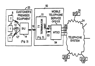
Figure 2 shows an emhoA;ment of the present
invention which is an interim configuration between the
total ATM system of the above cross referenced patent
applications and the present PCM based world telephone
system. Here the focus is on a subset of the prior system
as illustrated by Figure 1 with the conversion between ATM
cells and PCM signals occurring closer to the subscriber's
end of the system than discussed with respect to Figure 1
and in the cross-referenced patent applications of the same
applicant. In this embodiment, the customer premises
equipment 20 and the world telephone system 24 are the same
as in Figure 1. At the head end of cable 16, in place of
switching functionality 22 of Figure 1, there is a new
subsystem 50 that includes a Tl terminator unit 51 and a
~.u .!~LO PCT~S94/06717
2 1 65424
Mobile Telephone Service Office (MTSO) 54. Tl terminator
unit 51 is connected to the head-end of TV cable 16 and
communicates with MTSO 54 via up and down signal lines 53
and 52, respectively. MTSO 54 in turn communicates with
the world-wide telephone system 24 by means of cables 56,
which in most installations are leased lines.
The function of T1 terminator unit 51 is two
fold. First it performs the operations discussed above of
fiber terminator unit 28. In addition it takes the upward
bound ATM cells from SIU 14 and converts them into PCM/T1
carrier signals that are commonly used be the telephone
companies. The PCM/Tl carrier signals are then transferred
to MTSO 54 (typically, a cellular telephone switching
office which is tied to the telephone system via leased
lines 56 and which also receives signals independent from
those of the present invention via radio links from
individual cellular telephone hand-sets) for delivery to
and from the public switched telephone network 24. In the
downward direction MTSO 54 hands off the Tl/PCM carrier
signals from telephone system 24 to Tl terminator unit 51
which also performs the reverse transformation of those
signals to ATM cells for delivery to SIU 14.
For simplicity, Figure 2 illustrates the present
invention in a system wherein the subscriber is connected
solely to the world-wide telephone network 24 via a cable
TV system that feeds and receives signals from MTSO 54.
In Figure 3a, SIU 14 of Figures 1 and 2 is
expanded to show four subsystems thereof to illustrate the
connection of the subscriber's cordless telephone units 8
and 8' to both the cable TV system of Figure 2 and to the
subscriber's individual twisted-pair telephone line 10 at
the subscriber's site. (This concept is discussed in more
detail in the above-referenced patent application by the
same inventor entitled "Cell Based Wide Area Network
WU Y4/~8 PCT/USg4/06717
21 65424
11
Alternative Acc ^.aS Telephone and Data System", serial
number 07/953744, filed September 29r 1992.) As shown
here, SIU 14 includes software defined transceiver 601
(which is ~iR~lcsed in additional detail in conjunction
with Figure 13 below) for communicating with cordless
telephones 8 and 8', cable TV modem 108, telephone
interface unit 62, and microcontroller 72. For purposes of
discussion with this figure, cordless telephones 8 and 8'
each transmit and receive in the same mode, i.e. all ATM
mode or all a serial signal non-cell mode -- there is no
mixed mode transmission. Other than that limitation the
software defined trAn-c~iver 601 can ~ Gl L multiple
subscriber terminals simultaneously.
15The communication between terminals 8 and
software defined transceiver is via antenna 600 and
diplexer 602, together with programmable receiver 606 and
transmitter 624, each of which is ~o..LLolled by digital
signal processor 610 and 620, respectively. Additionally,
20each of processors 610 and 620 look to digital control 628
for the necessary parameters for receiver 606 and
transmitter 624, and, if wireless terminals 8 are other
than ATM mode devices, for the necessary control
information to convert the upstream serial signals to ATM
cells and to perform the reverse conversion from ATM cells
to the neC~c~Ary serial signal for the downstream signals.
TV cable modem 108 is connected to TV cable 16,
30sending the upstream signals via 5-30 MHz transmitter 110
and receiving the downstream signals via 450 MHz receiver
118 in the way described in the cross referenced earlier
filed patent applications. The operation of modem 108 and
the other functions performed to transmit and receive
telephone calls via TV cable 16 have been described above
and in greater detail in this cross referenced pending
patent application.
~ u~ uul11
2 1 65424
12
Similarly, telephone interface unit 62 is
connected to telephone twisted pair 10 on the subscriber's
site. Also shown are a conventional telephone instrument
60 and local exchange demarcation device D which optionally
connects the subscriber's on site twisted pair wiring 10 to
the local telephone company. This is described in more
detail in the above cross-referenced patent application by
the same inventor entitled "Method and Apparatus for
Sharing Common In-House Wiring to Permit Multiple Telephone
Carriers to Serve the Same Customer", serial number
07/949,434 filed September 22, 1992. Telephone interface
unit 62, to perform the usual ho~lsPkPering requirements of
such a unit, includes block 66 provides the housekeeping
(BORSHT) functions on the incoming and outgoing signals
which includes battery, overvoltage protection, ringing,
touch-tone decoding, signalling, and hybrid and
transmission. These are conventional telephone line
support functions under control of signals from controls
buffer 68 and measurç buffer 70. Telephone interface unit
62 also includes digital to analog converter (D/A) 85 and
analog to digital converter (A/D) 86 to interface between
BORSCHT unit 66 and microcontroller 72 to send signals to
and from the telco lines, respectively.
Since in the present invention the signal format
with which each of the software defined transceiver 610, TV
cable modem 108, and microcul.LLoller 72 communicate with
each other is ATM cells, telephone interface unit 62 must
also interface with microcontroller 72 with ATM cells.
Thus, in addition, D/A 8S and A/D 86 must also convert the
signals between ATM cells and Tl/PCM channels in both
directions, respectively.
The final component of SIU 14 is mi~u~ocessor
72 which includes a microprocessor and the usual supporting
RAM, ROM and address decoder collectively numbered 73, a
pair of signal buffers 80/81 in communication with each of
W094l3~28 PCT~S94106717
2 1 65424
the other components of SIU 14, and a pair of control and
measure buffers 82l83 also each in communication with each
of the other components in SIU 14.
s Since there are six possible combinations for
routing a call that originates at one point in the total
connected system of Figure 3a to any other point in the
connected system, microcontroller 72 performs that routing.
To perform all of the connections and the housekeeping
functions that are also required, microcontroller 72, as
shown here, is a 16+ state machine as outlined in the table
of Figure 3b. The microprocessor arrangement 73 determines
the destination and path of each byte. Given that
information, microprocessor arrangement 73 causes each byte
received from the originating unit (108, 62 or 601) in the
corresponding receive buffer 81 to be transferred via bus
74 to the transmit buffer 80 associated with unit 108, 62
or 601. Thus, the one of units 108, 62 and 601 which has
the byte to be transerred to another of those units writes
that byte to its associated receive buffer 81/81'/81". The
control and measure information to implement the above
transfers is handled using the associated control and
measure buffers 82 and 83, respectively, of each of units
108, 62 and 601. Referring to Figure 3b the allowable
states of microcontroller 72 can be seen to define the
desired operations.
The ouL~uL of the TV cable modem 108 is always in
the form of ATM cells and conversion of the ATM cells to
and from Tl/PCM channels occurs in the Tl Terminator Unit
51. The next several figures to be A i ~CltCe~ each
illustrate that conversion in different symbolic ways.
Referring next to Figure 4a there is shown a
conceptual diagram of the two different data transmission
domains that Tl termination unit 51 of Figure 2, and other
units shown and not shown in the various figures, converts
W094~0028 PCT~S94/06717
21 65424
_ 14
back and forth between depending on which direction the
signal is being sent, downstream A 146 (ATM to T1/PCM) or
upstream B 148 (ATM to Tl).
Figure 4b presents a timing diagram to illustrate
the linear mapping between the ATM and Tl/PCM domains. For
example, to map multi-byte ATM cell 166' into a Tl/PCM time
division multiplexed signal the individual consecutive
bytes of the ATM cell must be mapped into the time-spaced
byte arrangement of the Tl/PCM domain, i.e. the three
consecutive bytes of ATM cell 166' must be mapped into the
equally spaced, time multiplexed and separated Tl/PCM bytes
162, 162' and 162", respectively.
For convenience of illustration in Figure 4b,
each ATM cell has been shown to have three bytes when in
reality an ATM cell is made up of 53 consecutive 8 bit
bytes and each T1 channel is typically made-up of 8-bit
serial byte samples.
Figure Sc is a conceptual view of a random access
memory of 53 by 24, 8-bit bytes. If the conversion is from
Tl to ATM, then 24 bytes of data from each PCM channel are
read-in and stored top to bottom starting in the upper
right and progressing in vertical columns to the left with
each column being filed from the top in this illustration.
After the data is stored, then the corresponding ATM cells
are created by reading from the memory starting at the top
and reading vertically a column at a time beginning at the
column on the left in this illustration with only the data
from occupied PCM channels being converted into ATM cells.
Alternatively, if the conversion is from ATM to
T1, then the 53 ATM cells are read into the memory in
columns. If no ATM cell was present the column would be
left all zeros. Starting in the upper right and
~.v ~ J~O PCT~S94/06717
21 65424
_ 15
progressing to the left a cell at a time across the page
to the right. then the next lower row is read out, and so
forth. When the 53 ATM cells are stored then the T1
channels can be read out of memory starting in the right
corner and reading a byte at a time to the left for each
row and then doing the next lower row, and so forth.
To simplify interconnection with present day
cellular telephone switches (MTSO 54 in Figure 2) without
the necessity for the addition of hardware beyond that
described herein, ATM compliant cells that contain
signaling information are treated separately from those ATM
cells that contain voice and data information.
In Figure 2, the present invention starts with
ATM cells from cordless telephones and/or conventional
telephone signals, with different characteristics for each
of the connected systems at each end of the global circuit.
These cells are transmitted via a cable TV system and can
be converted into T1/PCM (or other types of signals) at the
point of interconnection with a cellular telephone
switching office, MTSO 54. The use of ATM cells and not
sending cells during silence periods allows serving a
larger population of cable users when the limited bandwidth
of the TV cable transmission path is the main constraint.
In this ATM cell transmission application, it is desirable
to limit the telephone signaling information to a single
cell.
Two alternative approaches for sending signaling
information are commonly used in practice. One approach is
that signaling bits can be "robbed" from the bit stream for
each voice carrying T1/PCM channel. Alternatively, a
single T1/PCM channel (Channel 23) can be reserved solely
for the transmission of signaling information. The second
approach is used in ISDN (Integrated Service Data Network)
implementation and thus is the preferred embodiment
W094/30028 PCT~S94/06717
21 65424
_ 16
described in detail below. However, one skilled in the art
could also use the "robbed bit" signaling approach in lieu
of the dedicated signaling channel approach to practice the
present invention.
The ISDN approach as implemented in the present
invention is illustrated in Figures 5a, 5b and 6 through
12c. Figure 5a is a block diagram representation of T1
terminator unit 51 of Figure 2 configured to implement the
ISDN approach in which the control signals are carried on
a separate channel from the voice and data signals. Here,
T1 terminator unit 51 is shown to include several functions
which is shown in block diagram form and in each block it
is also indicated in which subsequent figure the internal
details of that box can be found. Included are 1 through
n Tl side units 200 and 200n, respectively, each of which
communicate directly with MTS0 54 via the up- and
downstream lines 53 and 52, and 53D and 52n, respectively,
as discussed in relation to Figure 2. At the downstream
side of Tl terminator unit 51 are 1 through m TV cable side
units 202 and 202m, respectively, each of which communicate
directly with a TV cable 16 and 16m, respectively, as
discussed in Figure 2. Linking each of the TV cable side
units 202 and 202m with each of the Tl side units 200 and
200n for converting the voice and data carrying signals ATM-
Tl or Tl-ATM is packetizing processor 204. Similarly,
linking each of the TV cable side units 202 and 202m with
each of the Tl side units 200 and 200D for converting the
signaling carrying signals ATM-Tl or T1-ATM is signalling
transfer processor 206.
Since the upstream bandwidth of cable systems is
considerably more limited than the downstream bandwidth, it
is necessary to provide cable service within a particular
geographical area by means of a plurality of feeder cables
all connected to the same headend of the cable TV system.
In operation that generally converts to an isolated feeder
W094~0028 PCT~S94/06717
2 1 65424
-
cable per neighborhood. Thus a separate TV cable side unit
202 is needed for each common shared frequency division
multiplexed channel with each being able to handle perhaps
8-10 terminal devices using cell transmissions at the same
time. Similarly, each Tl side unit has a 23 channel
capacity limit and since, statistically not all of the
capacity of each of the TV cable side units will be usec ~t
any point in time, it is only necessary to provide
sufficient capacity in total of all of the Tl side units to
handle the statistical peak number of calls being handled
by the total combination of the TV cable side units.
Figure Sb is a block diagram that corresponds
with that of Figure 5a which is simplified in part in that
only one each of TV cable unit 202 and Tl side unit 200 are
shown, and expanded in part with the inclusion of added
functional blocks within each of packetizing processor 204
and signalling transfer processor 206 that illustrate the
conversion process of the up- and downstream signals ATM-Tl
and Tl-ATM in each block. In packetizing processor 204 in
the upstream direction block 250 shows the conversion of
ATM voice and data cells into Tl/PCM channel 0 through 22
signals, and similarly in the downstream direction block
242 shows the conversion of Tl/PCM channels 0 through 22
signals into ATM voice and data cells. In signalIing
transfer processor 206 in the u~Lleam direction the ATM
signalling cells conveying signalling data must be
converted to HDLC signalling format and placed in Tl/PCM
channel 23 (block 262) to be carried upstream, and
similarly in the downstream direction the HDLC signalling
formatted information in Tl/ PCM channel 23 is converted to
ATM cell format (block 256).
In Figure 6 Tl side unit 200 is ~YpAn~ upon
with the Tl link 52, 53 shown here as including DSU/CSU
interface unit 282. The link 214 to packetizing processor
204 is shown here as the combination of lines 240 and 252,
WU ~WLO PCT~S94/06717
21 65424
-- 18
whereas the link 216 to signalling transfer processor 206
is shown here as 254/264 for later individual reference.
As a T1/PCM signal is received from DSU/CSU 282 on line 208
it is directed to signal retimer 288 (only one of which is
necessary for all of the T1 side units, which is also the
case with respect to DSU/CSU 282) which is discussed in
greater detail with respect to Figure 7 and to a serial-in
parallel-out buffer 314. The purpose of retimer 288 is to
synchronize the T1 signals here with those of the telco
since the T1 telco signals must be very precise and the
output bus (see Figure 7) from retimer 288 is directed to
both signalling transfer processor 206 and packetizing
processor 204. From serial-in parallel-out buffer 314 the
downstream Tl/PCM channel signals are placed on bus 308 and
for direction to parallel-in parallel-out buffers 310 and
316 to direct channel 0-22 signals to packet processor 204
and the channel 23 signals to signalling transfer processor
206. Similarly the upstream signals from packet processor
204 and signalling transfer processor 206 are received by
parallel-in parallel-out buffers 312 and 316, respectively,
from which they are placed in signal bus 308 for transfer
to parallel-in serial-out buffer 318 for transfer upstream
via DSU/CSU 282. All of these functions are conducted
under the control of microcontroller 296 and the included
processor 298, EPROM 300, RAM 302 and ROM 304. Also shown
here are semaphores 320, 320' and 320" to synchronize the
timing of the transfer of signals between Tl side unit 200
and each of signalling transfer processor- 206 and
packetizing processor 204.
Retimer 288 is further expanded in Figure 7. The
Tl signals from the telco are time synchronous so that it
is necessary for the upstream data stream to match this
data rate. The signal on line 208 is the downstream signal
from DSU/CSU 282 from the telco which is made up of 192
bits in the form of 24 data channels, each of 8 bits, with
an added sync bit which may be either "1" or "0". That
W~Y4/~W~ PCT~S94/06717
2 1 65424
19
downstream signal is applied to AND gate 354, clock
separator 350, and data validity checker 368. Clock
separator 350 recreates a clock rate pulse from the
incoming data signal and applies that pulse to AND gate
354, modulo 192/193 counter 362, and data validity checker
368. The signal from AND gate 354, in turn is applied to
modulo 24x12 counter 360 and AND gate 364. Counter 362
then counts to either 192 or 193, depending of the state of
the sync bit. The modulo 192/193 count from counter 362
and the reclocked data stream from AND gate 354 in AND gate
364 creates the syncopated clock signal on line 366. Data
validity checker 368, using the reconstructed clock signal
from clock separator 350 and the incoming data stream
checks the data stream for the presence of unwanted
patterns and generates a reset signal on line 370 if a
problem is detected. Data validity checker 368 also
generates a frame start pulse on line 372 to define the
start time of each 192 bit data frame. The reset signal
from data validity checker 368 is also applied to the
modulo 24x12 counter 358 to trigger the start of the count
to generate a frame 23 valid signal on line 360. Timer 288
also includes a local clock that is controlled by a crystal
oscillator VXCo 380 that nominally operates at 8 times the
desired clock signal to gain additional edge resolution.
The 8x clock signal is brought out on line 382 and is
applied to divider 38~ to provide the desired 2.048 Mb/s
clock signal on line 386. Line 386 is also connected to
up/down counter 390, together with the syncopated clock
signal on line 366, to generate a correction signal to be
applied to VXCo 380 to correct the signal from the local
oscillator. Then for purposes of simplicity, lines 360,
366, 370, 372, 386 and 382 are considered bus 294 in Figure
6.
In Figure 8 there is shown a simplified Tl side
unit 200 that contains retimer 288 with the syncopated
clock line 366, 2.048 Mb/s clock line 386 and the 8x clock
W094t300~ PCT~S94/06717
~ 1 65424
- 20
line 382 each feeding a corresponding bus 404, 402 and 400,
respectively, for distribution for each of the T1 side
units 200 included in the Tl terminator unit 51.
In Figure 9 TV side cable unit 202 is shown in
greater detail with TV cable 16 shown to the left in
communication with the TV cable modem which consists of
high/low filter 422, high frequency upstream transmitter
450, low frequency downstream receiver 426, the
corresponding frequency control blocks 458 and 462,
respectively, which are controlled by microcontroller 434
via data bus 432 for setting the operating frequencies for
the selected band for the signals to and from the
subscriber. An downstream ATM cell from receiver 426 is
transferred to serial-in/16 bit parallel-out buffer 430
(with 16 bits or more being selected to give more
resolution for setting the frequencies of transmitter 450
or receiver 426) from which it is applied to data bus 432
and in-turn transferred to parallel-in/parallel-out buffer
442 for transfer to packetizing processor 204 via bus 248
if the ATM cell contains voice or data information. In
reverse, an upstream voice or data signal from the
subscriber is received from packetizing processor 204 via
bus 246 by parallel-in parallel-out buffer 444, which in
turn supplies that signal to bus 432. From bus 432 it is
applied to 16 bit parallel-in serial out buffer 446 for
application to transmitter 450, the high pass filter in
filter 422 and then to TV cable 16.
If the signals up- and downstream containing
signalling and address information then they are exchanged
with signalling processor 206 by microcontroller 434 which
receives or delivers then, from or to the transceiver
section discussed above via bus 432. Mi~o~ocessor 434,
in order to determine if the ATM cell currently on bus 432
contains signalling information and is to be directed to
signalling processor 206 examines the signalling bit in the
wog4/30028 PCT~S94/06717
21 65424
_ 21
header of the ATM cell and if it is set then ATM cell is
directed to signalling processor 206. To accomplish that,
the ATM cell is read into the ROM of microcontroller 434
for deliver to bus 435 and to address decoder 436 and
s parallel-in parallel-out buffer 445 for delivery to
signalling processor 206.
Also shown in Figure 9 are semaphores 320, 320'
and 320" to synchronize the timing of the transfer of
signals between TV cable side unit 202 and each of
signalling transfer processor 206 and packetizing processor
204.
Figure 10 is a hardware block diagram of
15signaling transfer processor 206 of Figures 5a and 5b.
This unit consists of a parallel-in/parallel-out buffers
(472, 474, 476, 478) and a semaphore flag S that is
associated with each one of said TV cable side units 202
and each T1 side units 200 (here four such buffers are
shown since the example of Figure 5a includes two of each
of the TV and Tl side units). Each of the buffers supplies
and receives, as appropriate, a signal to and from data bus
471 under control of microcontroller 470 which manipulates
the signals in the various buffers as per the flow diagrams
identified in Figure 5b. Additionally, each of the
semaphore flags is read and set by the microprocessor of
microcontroller 470 to coordinate the timing of the data
conversions and transfers performed here and the transfer
of data at the interface to the various TV and T1 side
units.
Similarly, Figure 11 is a hardware block diagram
of packetizing processor 204 of Figures 5a and 5b. This
unit consists of a parallel-in/parallel-out buffers (504,
35506, 508, 510) and a semaphore flag S that is associated
with each one of said TV cable side units 202 and each T1
side units 200 (here four such buffers are shown since the
W094~0028 PCT~S94/06717
21 65424
_ 22
example of Figure Sa includes two of each of the TV and T1
side units). Each of the buffers supplies and receives, as
appropriate, a signal to and from data bus 502 under
control of microcontroller 500 which manipulates the
signals in the various buffers as per the flow diagrams
identified in Figure 5b. Additionally, each of the
semaphore flags is read and set by the microprocessor of
microcontroller 500 to coordinate the timing of the data
conversions and transfers performed here and the transfer
of data at the interface to the various TV and T1 side
units.
Figures 12a through 12c are provided to
illustrate the operation of the semaphore system of the
present invention and how they function between each of the
pair of units where they are used as discussed generally
above. For purposes of illustration the interaction
between the semaphores of packetizing processor 204 and TV
cable side unit are used in the simplified block diagram of
Figure 12a. Here there is shown a microprocessor 434 and
S00 on either side of the interface with a single semaphore
320 shared between them, unlike what might have been
mistaken in Figures 9 and 11 as there being a first
semaphore talking to a second semaphore on each side of the
interface.
Figures 12b and 12c are flow charts detailing the
operation of microprocessors A and B (S00 and 434,
respectively) with respect to semaphore 320 in the
interchange of data between the two units from the
individual points of view of microprocessors 500 and 434 in
Figure 12a, respectively. Figure 12b is a flow chart that
describes the operation of microprocessor 500 and its
interaction with semaphore 320 to control the exchange of
data with the unit controlled by mi~o~ocessor 434. The
decision flow begins at block 520 with mi~G~ocessor A
(500) waiting for the next allowable interval. When that
w094/30028 PCT~S94106717
21 65424
23
time arrives, microprocessor A checks the state of the
shared semaphore (320) with microprocessor B (434) (block
524). If semaphore 320 (block 526) is set to zero then no
data is available (block 542) and microprocessor A
concludes that there is no data to be transferred from the
unit controlled by microprocessor B (434) (block 546) and
control returns to block 520 to -~ait the next allowable
polling interval.
If semaphore 320 is set to "l", then control
proceeds to block 532 where it is noted that there is data
available with microprocessor A proceeds to transfer the
data in register B (442) in the unit of microprocessor B to
register A (506) within the same unit as microprocessor A
(block 536). Following the transfer of the data between
the registers, microprocessor A resets semaphore 320 to "0"
(block 538) and control is returned to block 520 to await
the next allowable polling interval.
Considering the interface operation from the
point of view of mi~GpLocessor B (434), refer now to
Figure 12c. The process begin at block 560 where
microprocessor B awaits the next allowable polling interval
during which it proceeds to check the status of semaphore
320 (block 564). If semaphore is set to "0" (block 568),
microprocessor B next checks for data that it has that is
awaiting to be transferred to the unit of microprocessor A
(block 578). If no data is present, then the semaphore is
left set to "0" (block 590) and control is returned to
block 560 to await the next allowable polling interval.
If the test at block 578 indicates that there is
data awaiting to be transferred, then that data is
transferred from register B to register A (block 584), the
semaphore is set to "l", and control is returned to block
560 to await the next allowable polling interval.
W094~ PCT~S94/06717
21 652424
At block 568 if the semaphore is set to "1"
microprocessor notes that register A has not accepted a
previous data transfer and the delay between sending the
next data packet may have to be extended or there is some
other problem, e.g. there has been a failure of the
semaphore (block 574), and then control is returned to
block 560 to await the next allowable polling interval.
For purposes of illustration Figures 12a through
12c only discuss the semaphore operation for what in the
overall system operation would be an upstream data
transfer. When there is a downstream data transfer between
the same units, the interaction between then with respect
to the semaphore is the same with the function of
microprocessors A and B being reversed. Further, the
operation of the semaphores is the same between any two
units in the above describe system is the same as that
described here for these two units.
Another feature of the present invention is the
broadening of the earlier concepts disclosed in Figure 2,
as well as the cross-referenced pending patent applications
of the same inventor, by providing the capability for
supporting multiple alternative terminal air interfaces
between subscriber cordless devices 8 and SIU 14. To fully
accomplish this goal, SIU 14 is modified to provide the
necessary flexibility to support the use of an ATM cell
based and any non-cell hAc~A cordless devices 8 by the same
SIU 14, unlike the originally described operation where
multiple cordless devices of the same cell or non-celled
hAceA configuration could be handled simultaneously by the
same SIU 14. Thus in this configuration, SIU 14 may also
support one or more markedly different protocols and
arrangements now in place and used by currently available
and future cordless devices 8 until a common stAnAArd is
achieved, if ever.
WU ~C /.)W~ ;'l'IU~Y4/UO'll'I
21 65424
Thus, SIU 14 in the preferred configuration could
have been a fixed wired configuration in Figure 3a,
however, if the software defined transceiver as shown in
Figures 3a and 13 is used for either application, it would
also be possible to program the SIU to operate either in
the preferred format with multiple subscriber units each of
the same cell transmission mode, or in the secondary
embodiment with the capability of supporting one subscriber
terminal at a time wherein that terminal can be of any cell
based or non-cell based format. However, if the processing
of the signals is performed using fast Fourier transforms
it is also possible to interface with multiple terminals
each in the same signal format but transmitting at
different frequencies.
This arrangement thus allows support of both ATM
cell-based and non-cell-based devices, irrespective of the
different interface standards present, but with only one
being used at any instant in time. This freedom of choice
thus allows a transitional multiple mode capability so that
other PCS and cellular type telephone instruments can also
be used with the system of the present invention. To do
this, SIU 14 of Figure 13 converts conventional serial
signal streams from PCS cordless devices into compatible
ATM cell based signals that become a universal interface
signal with Tl terminator unit 51.
The concept of dual mode subscriber terminal
devices is well known with several manufacturers having
announced dual mode cellular telephone products. Generally
one of the two modes is cellular AMPS (Advanced Mobile
Phone System) while the other is a PCS technology. Unlike
the case where the circuitry and ~G~Lamming that must be
replicated in each cordless terminal unit to operate in
each mode varies by the nature of the particular mode
combination chosen, the present invention creates a
multimode capability in SIU 14 and not the subscriber's
2 1 62~424
cordless terminal instrument.
As discussed above, the preferred operational
mode of the present invention is the use of ATM cells down
S to the subscriber's cordless terminal, while secondary
modes might include one or more of the PCS stAnAArds, such
as DECT, CT2, GSM or other non-cell forms of PCS. of
course when SIU 14 is supporting several different modes of
signal transmission, a single SIU 14 would be able to
support only a single mode at a time. The capability to
support multiple simultaneous conversations as described in
the above cross referenced related patent applications can
only be performed by a single SIU 14 in the preferred
operational mode.
The embodiment supporting a multiplicity of
different air interfaces with cordless subscriber devices
8 is implemented, as discussed below in relation to Figures
13 and 14, by transforming, as n~ceCcAry~ the signals from
the various devices 8 to a single signal format for
transmission to a remote cellular switching center, e.g.
MTSO 54. The key concept here is the realization that
while each of several personal communications air
interfaces are in use or proposed, each have totally
2S different signal and protocol requirements. Upon closer
examination, however, it is noted that those requirements
can be broken down into common functions -- a generic
transmitter, a generic receiver, and a generic processor.
The transmitter and receiver can each be instantly software
definable since each operates at a limited number of
frequencies. While these frequencies are different for
each of the PCS systems they are sufficiently clustered so
that a single frequency agile unit can be designed to meet
the needs of each system. The number of center frequencies
for the existing and proposed PCS systems is quite limited,
there are only about two bAn~s, 900 MHz and 1800 MHz which
can easily be accommodated in the same unit. It is also
r~ u~ vv ~ ~ ~
~ . v ~ ~
2 1 65424
_ 27
possible that the receiver could even be a homodyne
receiver that does not need an IF, but that is not
mandatory. The processor and the logic is the easiest part
of the equation in that it potentially requires only
different software for each system. Thus, a single
hardware SIU 14 can de designed to appear to be one or more
software definable SIUs.
The main building blocks of each of the existing
and proposed PCS systems are:
1. RF Center Frequency Selection
Almost all of the new generation personal
communications terminals tend to operate in the
frequency range of 800 to loO0 MHz or 1800 to
2200 MHz. Local oscillators, frequency
synthesizers and similar functions may all be
served by a common frequency agile module, with
plug-in filters and a diode switch to select the
filters.
2. Diplexing Selection
All non-cell format terminals can be divided
into two classes of diplexing, Time Division
Diplexing (TDD) and Frequency Division Diplexing
(FDD). In TDD the transmitter and the receiver
are sequentially connected to a common antenna to
provide the illusion of simultaneous transmission
and reception while the FDD approach requires
carefully match filters.
3. Transmitter Selection
Hand held cellular devices operate at a 600
mW level and, the smaller PCS devices operate at
100 mW and less. Dynamic power reduction is
generally used and is of primary importance in
certain CDMA approaches necessary to maximize the
~ . V; .~J ~ D r~ ~ l u ~ vv ~ ~ ~ 2 1 65424
28
numbers of users on an rf channel. The short
ranges used with the present system allow much
lower power densities than found in most
transceiver devices designed for longer range
objectives than needed to reach an in-house
Subscriber Interface Unit, generally less than 60
meters.
4. Receiver Selection
The key receiver variable is bandwidth.
Most PCS systems use a broa~hAn~ channel that is
in turn time subdivided into separate channels.
Diode switched filters allow the matching of the
bandwidth to the application.
5. A/D Conversion
The output of the receivers can be handled
in a generic manner by an analog/digital
conversion of the received signal and its
quadrature component sampled at a rate
commensurate with the symbol rate used.
6. A/D Output
The output of the receiver after the analog
to digital process, is a set of paired digital
values generated at the sampled data rate
a~p~G~iate to the incoming symbol rate.
7. Digital Signal Processing (DSP)
The digital stream containing measurements
of the two quadrature signal components of the
received waveform are next pro~sce~ using a
general purpose pror~c~or to produce the desired
outgoing digital signal. The term DSP is
intended only in an overall sense, defined to
include constellation fitting, interpolation and
control as well as forward error correction,
W094/30028 PCT~S94/06717
21 65424
- 29
voice dynamic range expansion, dPco~ing of
signaling commands, etc.
In summary, a feature of the present invention
creates a generic transmit/receive capability wherein by
changing parameter settings causes the structure of the SIU
to be changed to match a different air interface as needed.
While it is obvious that it is less eYp~n~ive to restrict
manufacture to a single s~nA~rd, permitting a single SIU
instrument to serve any of several different PCS/cellular
formats is considered to be an economically advantageous
feature to justify the additional complexity and cost.
While this ~iccllcsion speaks in terms of generic
transceivers operating in the 800 to 100 MHz range and the
1800 to 2200 MHz range it is obvious to one skilled in the
art that other frequencies could be chosen as well such as
5400 MHz, or even 40 MHz as used for cordless telephones.
Referring now to Figure 13 there is shown a
programmable SIU 14 (see Figure 2) for use with various
non-cell based cordless subscriber units 8, one at a time.
To support the simultaneous use of multiple terminals 8 of
different signal transmission modes, SIU 14 would have to
create a separate virtual transceiver for each terminal
transmission mode in use at that time. As shown, software
defined transceiver 601 includes a receiving digital
processor 620 coupled to programmable transmitter 624, a
sending receiver 606 coupled to sending processor 610, and
a diplexer 602 and associated antenna 600 for transmission
to and from subscriber terminal 8. In the sending
direction, subscriber terminal 8 transmits a signal which
impinges antenna 600, is then directed by diplexer 602 to
programmable receiver 606, to sending digital processor 610
to be converted into ATM cells as necessary and written to
buffer 81" in microcontroller 72 (see Figure 3a). In the
receiving direction, the ATM cell to be received is read
~. v, ..__U~o ~;lIU:~Y~lU~
21 65424
from receiving buffer 80" of microcontroller 72 (see Figure
3a) by receiving processor 620 where it is converted to the
signal mode of terminal unit 8 if it is other than ATM
hAs~A. The signal from receive processor 620 is then
transferred to receive transmitter 624, applied to diplexer
602 and antenna 600 and transmitted to terminal 8.
Additionally, the function of each of the above-described
units, other than antenna 600 and TV cable modem 108 are
controlled by digital controller 628 which is programmed to
adjust, or program, the operation of each of those units in
response to the type of terminal device being used by the
subscriber and to convert to and from ATM cell based on the
transmission mode of terminal 8.
The key to the operation of programmable SIU 14
is that the mode of operation for both upstream and
downstream transmission is defined by the operational mode
of the terminal 8 of interest. In operation then, digital
controller 628 of software defined transceiver 601 of
Figure 13 is programmed sequentially look for each expected
form of modulation and data formats in the receive mode.
This operation of software defined transceiver 601 of
Figure 13 is illustrated in block diagram form in Figure 14
in simplified form. When there is a signal either send or
receive, digital controller 628 initially trys the default
mode (Mode #l) of block 652. Receiver 606 is checked for
receipt of an RF signal (block 656), if one is received the
characteristics of the signal is checked against those for
Mode #1 (block 662), and if the characteristics match then
Mode #1 is selected (block 666). If either the RF signal
is not received (block 656) or the received signal is not
valid (block 662) control is directed to block 668 to try
Mode #2. The same tests as for Mode ~1 are performed for
Mode #2 in blocks 672 and 678, with Mode #2 being selected
if both tests are successful (block 684), otherwise control
shifts to block 686 to try Mode #N with the tests being
conducted again in blocks 690 and 694 with Mode #N being
~Og4~ r~lIU~lU~
21 65424
_ 31
selected if the tests are successful (block 700) or if
either test fails control is returned to block 652 to
restart the process for Mode #1. As stated above, this
procedure continues until the correct mode is determined
and established by digital controller 628.
The preferred embodiment here and in the above
cross-referenced patent applications by the same inventor
each uses an ATM cell format that is an "ATM compliant
cell" format that differs from full st~n~Ard ATM cell
format in that some of the payload space is reserved to
contain additional addressing space that is ne~ to
eYp~ the address space beyond the stAnd~rd 5-byte ATM
header to permit the addressing of cells to specific
subscriber terminal devices. The additional address bits
in the ATM compliant cells are invisible to the
conventional ATM switches, thus allowing there use with
conventional ATM networks as well. additionally, as used
in this application the term compliant ATM cells includes
cells that contain control signals and which may be of a
different length than the cells that contain data or voice
information.
Although the descriptions above primarily discuss
the use of present generation implementation techniques,
some specific technologies involved in the preferred
embodiments of the present invention are e~r~cted to change
as time evolves. Further, as will be understood by those
familiar with the art, the present in~ Lion may be
embodied in other specific forms without departing form the
spirit or essential characteristics thereof. The scope of
the present invention therefore in its full interpretation
is only to be limited by the scope of the claims appended
hereto.