Note: Descriptions are shown in the official language in which they were submitted.
WO95/~6~ 216 ~ 5 6 4 PCT/GB94/~602
~ -- 1 --
DISPERSION COMPENSATION IN AN OPTICAL
COMMUNICATIONS SYSTEM
The present invention relates to methods and apparatus
for compensating for dispersion in optical communications
systems, and in particular to methods and apparatus employing
optical phase conjugation.
In order to have a high transmission capacity, an
optical communications system must have low dispersion, this
means that pulses of light travelling along the waveguide,
generally an optical fibre, of the optical communica-tions
system should not suffer significant distortion. This
distortion may arise from a number of sources. If the
optical communications system employs multi-mode fibre, each
of the different modes will have a different group velocity,
15 thus modulated signals, i.e. pulses of light passing down the
multi-mode optical fibre, which are made up of a number of
different modes of the waveguide will experience a different
group delay from each of their modes. This causes a pulse
formed from more than one mode to spread out as it
20 propagates, and is called intermodal dispersion. Once
consecutive pulse have spread out so that they are no longer
distinguishable, one from the other, the information
transmission limit of the optical communications system has
been reached. This limit is expressed as a bandwidth
25 distance product since it will be reached at a higher bit
rate for a shorter optical communications link. Intermodal
dispersion between the modes of multi-mode fibres is one of
the reasons why modern optical communications systems have
moved to the use of single mode optical fibre which, since it
30 only supports one optical mode, does not suffer from
intermodal dispersion.
However single mode optical communications systems do
suffer from pulse spreading due to the small, but finite
bandwidth of the optical source employed. This type of pulse
spreading is called chromatic dispersion, and is due to two
effects. Firstly, material dispersion is present because the
refractive index of a dispersive medium, such as silica from
SU~STITUTE S~EET (RUI.E 26~
W095l~6~ ~6~ - 2 - PCT/GB94/00602
which optical fibres are typically made, depends on
wavelength. Secondly, waveguide dispersion, since the
propagation characteristics of the single mode supported by
a single mode fibre also depend on wavelength. Since the
material dispersion of silica is positive at most wavelengths
of interest for optical communications systems, and the
waveguide dispersion for single mode fibres is negative,
these two effects can be carefully balanced in a well
designed optical fibre so as to give zero total, chromatic
dispersion at the operating wavelength of the optical
communications system.
The vast majority of optical communications systems
which have been installed worldwide contain single mode
optical fibre which has been designed for use in the 1.3~m
low loss window, and as such has low chromatic dispersion at
this wavelength. In recent years the rapid development of
erbium doped fibre amplifiers (EDFA) has meant that fibre
loss, and thus the power- budget of optical communications
systems, is no longer the fundamental limit to achievable
20 transmission distance. However these EDFAs are only operable
in the 1.55~m optical transmission window so that if existing
optical communication links are to be upgraded, for example
to operate at higher bit rates, these systems must operate in
the 1.55~m at window, over optical fibre designed for use at
1.3~m. Thus the fundamental bandwidth distance product
transmission limit when upgrading an existing optical
communications system is that imposed by dispersion.
Furthermore, even for systems having fibre designed for use
at 1.55~m, as very high bit rates are approached, unless very
narrow linewidth, externally modulated lasers are employed,
dispersion again is the fundamental limit to transmission
capacity.
A number of methods of compensating for dispersion are
known. In one such technique the optical signal, at the
transmitter end of the optical communications system, is
deliberately distorted before being launched into the optical
fibre. The distortion imposed upon the optical signal must
W095/~3 21 6~ ~ 1 PCT/GB94/~602
be calculated so as to be compensated by the dispersion that-
the optical signal subsequently suffers during propagation
along the optical fibre. An example of such a technique is
that disclosed by Koch and Alferness in "Dispersion
Compensation By Active Predistorted Signals Synthesis"
Journal of Lightwave Technology, volume LT-3, no. 4, August
1985. In order to successfully apply these techniques the
transmission characteristics of the particular optical fibre
employed, and the length of the transmission link need to be
10 known so that the predistorted signal can be correctly
synthesised. Generally the optical source employed in these
systems needs to be sophisticated, and thus complex, 80 a8 to
allow independent control of the amplitude and frequency of
the optical signal. The problems inherent in predistortion
15 dispersion compensation systems are considerably exacerbated
for higher bit rate systems, where indeed dispersion
compensation is of greatest importance.
In a second, known dispersion compensation technique
a negative dispersion optical fibre is employed to compensate
either at the transmission end, or at the receiver end of the
optical link for the positive dispersion suffered by optical
signals propagating along the transmission optical fibre.
When optical signals at 1.55~m are transmitted along a
transmission optical fibre having a dispersion zero at 1.3~m,
2S the signals will suffer positive dispersion i.e. the sign of
the differential of their group delay with wavelength, will
be positive, and will typically be of the order of
17ps/km/nm. Single mode optical fibre can be specifically
designed to have a large negative chromatic dispersion, by
choosing the waveguide parameters to give large negative
waveguide dispersion, for èxample a fibre having a core of
small diameter and high refractive index will have negative
waveguide dispersion. Such a scheme was employed by
Izadpanah et al in "Dispersion Compensation In 1310nm
35 Optimised SMFs Using Optical Equaliser Fibre, EDFAs And
1310/lSSOnm WDM" Electronics Letters, 16 July 1992, volume
28, no. 15, page 1469. Izadpanah et al employed a specially
WO 9~1.3C~3 PCT/GB94/00602
2~6556~ ~
designed negative dispersion fibre having a di~persion of
-45ps/km/nm. The length of negative dispersion fibre
required was approximately one third of the length of the
transmission link over which dispersion was being
compensated. Such large lengths of additional fibre are
clearly inconvenient and expensive. Furthermore due to the
high level of doping used in the core, and the small core
size this fibre had a relatively high loss, so that
amplification of the optical signal is essential, even if the
10 bit rate of the system is not increased.
A third form of dispersion compensation has been
theoretically proposed by Yariv et al in "Compensation For
Channel Dispersion By Non-linear Optical Phase Conjugation"
Optics Letters, volume 4, no. 2, February 1979. Yariv et al
15 proposed that by generating an optical phase conjugate
replica of the optical signal after it has passed through one
half of the optical transmission link, and launching this
phase conjugate replica into the second half of the optical
transmission link, the effects of the dispersion suffered by
the optical signal in the first half of the link will be
reversed and the optical signal will be restored to its
original shape. This technique relies on the time inversion
of the group velocity dispersion of the optical signal caused
by phase conjugation, and thus requires that the dispersion
25 in the second half of the optical transmission link is the
same as the dispersion in the first half, if it is to be
fully compensated for.
Yariv's proposal has been implemented in an optical
communications system ~y employing non-degenerate four wave
30 mixing (NDFWM) in dispersion shifted fibre (DSF) to provide
the necessary optical phase conjugation. In this case the
phase conjugate optical signals travel in the same direction
as the copropagating pump light and original optical signal.
This technique has been demonstrated by Watanabe et al in
"Compensation Of Chromatic Dispersion In A Single Mode Fibre
BY Optical Phase Conjugation~ IEEE Photonics Technology
Letters, volume 5, no. 1, January 1993 and by Jopson et al in
,. - 21 6S~6LI
-
"Compensation Of Fibre Chromatic Dispersion By Spectral Inversion" Electronics
Letters, 1 April 1993, volume 29, no. 7. In both cases long lengths, over 20km,
of carefully designed DSF were required. A DSF is a fibre which has been
designed to have zero dispersion in the 1.55~Lm telecommunications window, i.e.
5 its dispersion zero has been shifted from 1.3~1m to around 1.55~m. In addition to
this requirement, Watanabe and Jopson furthermore needed to arrange for the
wavelength of the pump light required for NDFWM in the DSF to be the same as
the zero dispersion wavelength of the DSF, in order to achieve sufficient phase
matching between the pump and the optical signals. This requirement for phase
10 matching over the 20km of the DSF is severe, and means that the wavelength ofthe pump light must be carefully controlled e.g. over 20km with a pump and signal
separation of 2nm the pump wavelength must be within approximately 1 nm of the
dispersion zero wavelength. Furthermore this requirement`becomes more severe
as the length of the DSF increases, and rapidly more severe as the wavelength
15 separation of the pump and signal is increased. The efficiency of conversion of the
optical signal to its phase conjugate replica achieved by both Watanabe and
Jopson is low, approximately -25dB in both cases. Thus the phase conjugate
signal to be launched into the second half of the optical transmission link is at a
very low level.
It has been suggested by Murata et al in "THz Optical Frequency
Conversion Of 1 Gb/s Signals Using Highly Non-degenerate Four Wave Mixing In
An InGaAsP Semiconductor Laser" IEEE Transactions Photonics Technology
Letters, volume 3, no. 11, November 1991, that Yariv's phase conjugation
technique for dispersion compensation could be implemented by employing a
25 semiconductor Fabry-Perot laser as the phase conjugating device. This suggestion
has not, however been demonstrated.
Another known technique for dispersion compensation is described in
"Chirping Compensation Using a Two-Section Semiconductor Laser Amplifier" -
Journal of Lightwave Technology, vol. 10, no. 9, Sept 1992, pages 1247-1254.
The present invention provides a method of compensating for dispersion in
an optical communications system, the method comprising the
PN~END~ S~E~
W095/~653 PCT/GB94100602
2165~ 64 6
steps of
i) positioning a semiconductor optical amplifier
between a first and a second length of optical
fibre,
ii) launching optical signals into the first length
of optical fibre,
iii) directing optical signals emerging from the
first length of optical fibre into the
semiconductor optical amplifier,
ivl supplying optical pump radiation to the
semiconductor optical amplifier so that the
optical signals and the pump radiation within
the semiconductor optical amplifier and
generate the phase conjugate of the optical
signals, and
v) launching the phase conjugate optical signals
into the second length of optical fibre.
The method of the present invention thus overcomes the
disadvantages inherent in using DSF to provide optical phase
conjugation, by employing a semiconductor optical amplifier.
These devices are of a short length, of order one hundred
microns, so that phase matching between the pump radiation
and the optical signal is easily achieved. Since
semiconductor optical amplifiers have gain, the efficiency of
30 the optical phase conjugation process is far higher than for
passive DSFs.
The applicants have surprisingly found the method of
the present invention successful in compensation for
dispersion in optical communications systems, despite the
fact that there is substantially no cavity enhancement of the
optical phase conjugation in a semiconductor optical
amplifier. The theoretical suggestion by Murata et al leads
WO9SI03~3 21 6S PCT/GB94/00602
- 7 -
the skilled man to expect that substantial cavity enhancement
of the four wave mixing process by a resonant structure, for
example a Fabry-Perot laser, is essential to the achievement
of sufficient optical phase conjugation efficiency. The
applicants have discovered, not only that this is not the
case, but that there are significant advantages in employing
a semiconductor optical amplifier rather than a semiconductor
laser. When a significant degree of cavity, or resonance,
enhancement is employed the pump and optical signal must both
be accurately controlled in wavelength so that they are
coincident with one of the cavity modes, thus requiring
accurate wavelength control over these signals. The pump
radiation wavelength in particular must coincide with that of
one of the cavity modes of the Fabry-Perot laser to injection
lock it, and these modes typically have an injection locking
bandwidth of only a few GHz. Furthermore the use of
resonance enhancement inherently places a limitation on the
modulation bandwidth that can be imposed on the optical
signal. This is because if the bandwidth of the optical
signal begins to approach the bandwidth of the cavity
resonance, the cavity resonance will act as a spectral filter
to the optical signal, causing distortion of the modulation
pattern of the optical signal. This effect will become more
severe as the modulation bandwidth of the optical signal
increases, and particular far more severe if the optical
signals are not transform-limited, for example if the
transmitter has significant linewidth or suffers from chirp.
A further disadvantage, inherent to all resonant devices, is
their instability under temperature variations or mechanical
vibration.
Preferably a semiconductor optical amplifier employed
in the method of the present lnvention has a variation in
gain with wavelength, caused by facet reflections, of less
than SdB i.e. the amplitude of the so called "gain ripple" is
less than SdB. The Applicants have determined that
semiconductor optical amplifiers having a gain ripple less
than 5dBs will not suffer substantially from the
WO55,~?~.'3 PCT/GB94/00602
2 1 65 ~ 6~ - 8 -
disadvantages of cavity enhancement, for example the optical
signal bandwidth restriction discussed above. As will be
described hereinafter such semiconductor optical amplifiers
do, however, benefit to a small degree from some cavity
enhancement.
Preferably the semiconductor optical amplifier
employed in the present invention has facet reflectivities of
less than 103. This effectively ensures that, for single
pass gains of up to 20 dB, the semiconductor optical
amplifier is a travelling wave amplifier, having no cavity
enhancement.
Preferably the wavelength of the optical signal and
the wavelength of the pump radiation are separated by at
least lnm. This ensures that the four wave mixing undergone
by the optical signals and the pump radiation is highly non-
degenerate. This is desirable since highly non-degenerate
FNM (NDFWM) is based on an ultra-fast intraband optical non-
linear gain process which has a very short response time,
less than lps, and thus allows the present wavelength
dispersion compensation technique to be applicable to optical
communications systems operating at bit rates up to tera bits
per second.
Advantageously the gain of the semiconductor optical
amplifier is saturated by the pump radiation. The applicants
have surprisingly discovered that operating the semiconductor
optical amplifier under saturation increases the ratio of the
phase conjugated signal to the background spontaneous
emission.
In addition, or alternatively, the semiconductor
optical amplifier is advantageously operated with a high
injection current. Although both the level of the phase
conjugated optical signals, and the background spontaneous
emission increase with increasing injection current, it has
been found that the rate of increase in the level of the
35 phase conjugated optical signal is greater than that of the
background spontaneous emission, so that the signal to
background ratio may be increased by increasing the injection
WOg5/036~ 21 ~ PCT/GB94/00602
current.
Although the optical pump radiation may be supplied to
the semiconductor optical amplifier via the first length of
optical fibre, advantageously the optical pump radiation is
supplied to the semiconductor optical amplifier from an
optical pump source co-located with the semiconductor optical
amplifier. This arrangement ensures that the optical pump
radiation does not suffer, for example from Brillouin
scattering in the first optical fibre.
Advantageously, the optical pump radiation supplied to
the semiconductor optical amplifier is generated within the
semiconductor optical amplifier. This may be achieved, for
example, if both the semiconductor optical amplifier and the
optical pump source are comprised by a semiconductor device
15 having wavelength selective feedback means, for example a
distributed feedback (DFB) laser, or a distributed Bragg
reflector laser. In this case the pump radiation for four
wave mixing, rather than being supplied to the semiconductor
optical amplifier from an optical pump source distinct from
the semiconductor optical amplifier, is generated by the
interaction of the wavelength selective feedback means with
the gain medium of the semiconductor optical amplifier.
Thus, in this case, a single semiconductor device, for
example a DFB laser, acts as both a source of narrow
linewidth pump radiation, and the non-linear medium in which
four wave mixing occurs. Hence only the optical signals are
injected into the single semiconductor device, and the phase
conjugated optical signals are extracted from the
semiconductor device. Preferably the wavelength selective
feedback means provide strong optical feedback only at the
pump wavelength, so as to avoid causing spectral filtering of
the optical signals, or the phase conjugate optical signals.
According to a second aspect of the present invention
there is provided an optical communications system comprising
a transmission path including a first optical fibre and a
second optical fibre, an optical signal source for launching
optical signals into the first optical fibre, an optical pump
W095/~6~ PCT/GB94/00602
2l6ss64 - 10-
source for generating pump radiation, and a semiconductor
optical amplifier having an input from the first optical
fibre and an output to the second optical fibre, wherein, in
use, the semiconductor optical amplifier receives the pump
radiation and the optical signals, after said signals have
propagated through the first optical fibre, and generates
phase conjugate replicas of the optical signals, which
replicas are launched into the second optical fibre.
According to a third aspect of the present invention
a semiconductor optical amplifier is used to provide phase
conjugation of optical signals in an optical communication
link and thereby to substantially compensate for dispersion
suffered by the optical signals during propagation along the
optical communications link.
Embodiments of the present invention will now be
described, by way of example only, with reference to the
accompanying figures, in which
Figure l(a) shows the output spectrum of a SOO~m
Fabry-Perot laser with the laser free-running, with 64mA
injection current, (b) shows the injection-loced spectrum of
the same laser with -6.7dBm light coupled into the device
from an LEC laser operating at 1.557249~m;
Figure 2 shows non-degenerate four-wave mixing in an
injection locked Fabry-Perot laser around the 5th resonance,
(a) shows the spectrum off-resonance, with the probe laser
wavelength between two FP modes, (b) shows the spectrum on
resonance, with the probe laser wavelength tuned to the peak
of the FP resonance;
Figure 3 shows non-degenerate four-wave mixing in an
injection locked Fabry-Perot laser around the 14th resonance,
(a) shows the spectrum off-resonance, (b) shows the spectrum
on resonance;
Figure 4 shows resonance profiles for (a) the NDFWM
conjugate signal, and (b) the probe laser signal, in an
injection-locked Fabry-Perot laser;
Figure 5 shows facet output powers, from a FP laser,
of the pump, probe and NDFWM conjugate signals(to short and
W095/~3 21 6~S PCTIGB94/00602
long wavelengths) at the peak of each resonance, as a
function of the pump probe detuning;
Figure 6 shows resonance lineshapes for a FP laser for
the pump, probe and NDFWM conjugate signal (short wavelength)
for (a) the 5th and (b) the 14th resonance away from the FP
resonance at which the pump is injected, the abscissae
showing the pump-probe detuning frequencies;
Figure 7 shows the theoretical variation of the
resonance enhancement and the bandwidth of cavity-enhanced
lO NDFWM with gain ripple;
Figure 8 shows the experimental arrangement for an
embodiment of the invention;
Figure 9 shows optical spectra measured at the output
of the SOA shown in Figure 8, (a) with the DFB signal, and
lS (b) without the DFB signal (offset by -lOdB);
Figure 10 shows eye diagrams for the arrangement of
Figure 8 for (a) the back-to-back arrangement, (b) lOOkm
transmission without dispersion compensation, and (c) lOOkm
transmission with dispersion compensation (measurements were
20 made using a 2.5Gbit/s optical receiver, with -26dBm received
power);
Figure 11 shows bit error rate curves for the back-to-
back arrangement, lOOkm transmission without dispersion
compensation, and lOOkm transmission with dispersion
compensation 2.488Gbit/s (215-1) NRZ pseudo-random se~uence;
Figure 12 shows the power of the phase conjugate
signal and signal-to-background ratio as a function of the
chip gain of a travelling wave amplifier (TWA).
Figure 13 shows phase conjugate power and signal-to-
30 background ratio as a function of the total fibre input power(pump+signal). (The curve is a guide to the eye).
The applicants have carried out experiments, and a
theoretical analysis, to determine the effect of cavity
enhancement on NDFWM. These experiments and analysis will
first be described, followed by a description of an optical
communications system according to an embodiment of the
present invention.
W095/03C53 PCT/GB94/00602
2 16S 5 6 l _ 12 -
A number of experiments have been carried out with
Fabry-Perot lasers i.e. devices having very high levels of
cavity enhancement, by injecting two signals, a pump and a
probe into these lasers, and tuning the wavelength of the
pump and the probe across the Fabry-Perot (FP) resonances of
the lasers. Figure la shows the output spectrum from a 500~m
Fabry-Perot laser, having 16 multiple quantum wells tMQW),
when the laser is free running, with 64mA injection current.
It can be seen from this figure that the output on resonance
is some 30dBs greater than off resonance. Figure lb shows
the output spectrum from the same Fabry-Perot laser following
injection locking with -6.7dBm light from the tunable pump
source.
Light from the probe source was coupled into the
Fabry-Perot laser, maintaining the input power constant at -
13.6dBm (coupled-in power). With the wavelength of the pump
maintained at 1.557249~m, the wavelength of the probe was
tuned through the FP resonances of the pump to longer
wavelengths, with up to 9.7nm (1.19Thz) detuning between the
two inputs. Output spectra with two inputs are shown in
Figures 2(a) & (b) (for -3nm, 370GHz detuning between the
pump and probe and in Figures 3(a) & (b) (for -9nm, l.lTHz
detuning); in both cases Figure (a) shows the spectrum off
resonance and (b) the spectrum on resonance. The effect of
the cavity FP resonances on the NDFWM is, qualitatively, very
clear: when the wavelength of the probe lies in between two
FP resonances (off resonance), no conjugate signals could be
observed, but tuning the probe to the peak of the FP
resonance causes a dramatic increase in the conjugate beam
30 power.
The optical power in the NDFWM conjugate beam (to
shorter wavelengths) and the probe laser outputs are shown in
Figures 4(a) & (b), respectively, as a function of the pump-
probe detuning. The powers were determined from the measured
spectra, but the system was calibrated to obtain actual facet
powers. Both the conjugate and probe beams show resonances,
corresponding to each of the 14 FP resonances, with narrow
W095/03653 PCT/GB94/00602
~ - 13 - ~1 6~ ~
linewidth. Though the peak-to-trough ratios for the probe
beam resonances are approximately equal to those of the
residual FP modes of the FP laser spectrum, the magnitude of
the conjugate beam resonances correspond to the square of
these amplitudes.
The optical powers of the pump, probe and NDFWM
conjugate beams (to both longer and shorter wavelengths) at
the peak of the resonances is shown in Figure 5. The most
important feature of the figure is the roll-off of the power
of the short wavelength conjugate beam. For detunings of up
to 0.9THz(7.2nm) the conjugate beam strength decreases at the
rate of approximately lOdB/decade. Above 0.9THz (7.2nm) the
conjugate beams strength decreases at the rate of
approximately lOdb/decade. Above 0.9THz there is a much more
rapid drop in optical power. The absolute power level of the
conjugate beam is at least an order of magnitude higher than
measured in similar experiments on travelling wave amplifiers
for simila_ input powers. In fact, for detunings up to
-0.6THz (4.8nm) the power of the conjugate beam at the output
facet is higher than the injected power in the probe beam.
The solid line shows the theoretically predicted NDFWM
gain (arbitrary scale) given by:
gFW~(~)a I ~( Ps~ , ~NL l2
l-z~rR 1 -
~
( 1 )where Ps,t is the gain saturation power of the amplifier and
P is the total optical power, ~NL is the non-linear gain
parameter, ~ is the pump-probe detuning, tR and r in are the
characteristic times of the physical processes giving rise to
the two terms, that is, carrier density 'population
pulsations' and non-linear gain. rR is the effective
recombination lifeline (including stimulated emission), and
r in is the intraband relaxation time. The theoretical curve
shown gave a good fit to the experimental data for a 16-well
strained layer travelling wave amplifier under similar
experimental conditions, with parameters rR=0.08ns and
WO 95/03653 PCT/GB94/00602
2~L6~ 14 - ~
~in=. 5Ps- The curve gives a reasonable fit to the data for
detunings up to 0.9THz, the relatively slow decay
(-lOdB/decade) arising from the combination of the fast decay
(20dB/decade) of the NDFNM due to population pulsations
(~ l/TR), and the almost constant level of NDFWM from non-
linear gain (~sl/~R).
The rapid decay of the conjugate signal for
frequencies above 0.9THz is due to two effects: (1) the
broadening of the resonance resulting from reduced modal
gain, and (2) the dispersion of the mode index, resulting in
a varying FP mode spacing. Since the enhancement in the
conjugate beam power results from the coincidence of both the
probe and conjugate beams with FP resonances, the latter
effect results in the two beams not being at resonance
simultaneously. This effect appears to be dominant, since
effect (1) would result in a sharp reduction in the probe
output power beyond 0.9THz detuning, which is not observed.
In order to quantify the enhancement in NDFWM
efficiency resulting from cavity resonances, the results
described in the previous section will be compared with
results on travelling wave amplifiers (TWAs) and DFB lasers.
For the TWAs, a pump and a probe beam were injected into a
device which had been anti-reflection coated on both facets
to s0.2%; the devices gave high single-pass gain (-20dB) with
<2dB residual Fabry-Perot ripple. For the DFB, a single
probe input was injected into the device, which was operated
well above threshold, emitting >lOmW power.
- It is necessary, however, to compare the results in a
way which removes the dependence on experimental details,
e.g. input powers and single-pass gain . Since the power in
the conjugate beam is, in 7eneral, described by the relation
PF~PI2P2, where Pl, P2, PF~ are the optical powers of the pump,
probe and FWM conjugate beams, coefficients ~out and ~in are
defined for the purposes of comparison in the following way:
PFWII~ OUt ~OUt- ( Pl~ OUt ) P2~ OUt ( 2 )
PFWM~ OUt il jn- (P" in) P2~ in (3)
where the subscripts 'out' and 'in' denote whether the power
WO95/~653 PCT/GB94/00602
_ - 15 - ~6
is the output facet power or the coupled-in input power. ~in
indicates the basic efficiency of a device for phase
conjugation, through this will depend on the single-pass gain
at which the device is operated. ~out gives a better
indication of the intrinsic efficiency of each type of
device, since this removes the dependence on single-pass
gain, and therefore will more clearly show the effect of FP
cavity resonances. Table 1 shows the values of ~Ou~ and ~in
for lT~z pump-probe detuning, for five measurements. Devices
numbered 1, 2 and 3 are two facet anti-reflection coated
amplifiers, device 4 is a DFB laser, and device 5 is a Fabry-
Perot laser. (In all the measurements, the weaker probe beam
was to longer wavelength of the pump beam).
Type Coupled Input ~0ut/mw2) (~i n / mw
Powers (dB) (dB)
Pl(dBm) P2(dBm)
1 2FC Amplifier -4.5 -9.2 -62.2 -14.2
2 2FC Amplifier -6.1 -10.1 -56.6 -2.6
3 2FC Amplifier -7.7 -12.2 -56.1 -2.1
4 3-Section DFB --- -60.7 ----
-9.3
Uncoated, -6.7 -30.7 +7.7
Injection-
Locked
The most remarkable feature of the table is that,
while the values of ~out for the TWA and DFB measurements are
relatively uniform, the value for the FP device at resonance
is -30dB greater. This indicates that the effect of the FP
cavity is to give roughly three orders of magnitude
enhancement in the NDFWM efficiency. There is considerably
less difference in the values of ~in owing to the much lower
gain in the F-P device, though as expected, there is less
uniformity for the TWA and DFB results.
WO9S/~C53 PCT/GB94/~602
2 ~65 S 6 ~ ~ 16 -
The results shown in Figure 4 reveal that the
resonance enhancement in the NDFWM occurs over a narrow
bandwidth, and this imposes a severe limitation on the use of
the effect, both with regard to the maximum bit rates and to
the ease of use. The output intensities of the pump, probe
and conjugate beam (short wavelength) for a small range of
detunings around the resonance are shown in Figure 6 for ta)
the 5th resonance and (b) the 14th resonance. The
experimental points for the probe and conjugate beams are
fitted using the following Airy-like functions:
Ipr = Ip~o {[1-RG]2 + 4RGsin2(~k.L)}l (4)
IF~ = IF~O ~[1-RGl2 + 4RGsin2(~k.L)}~Z (5)
where RG=~(R~R2).exp(gL) and Rl,R2 are the facet
reflectivities, g is the single-pass gain and L is the device
length. ~k is the wavevector detuning from the FP resonance,
and ~k.L=~(~f/~fFsR) where Af is the frequency detuning and
is the free spectral range of the FP modes. Equations
(4) and (5) are obtained assuming equal, uniform modal gain
and effective index for probe and conjugate beams, and
uniform pump power.
The parameter RG indicates the degree of feedback
within the Fabry-Perot cavity, and in particular the
magnitude of the gain ripple (i.e. ratio of the maximum to
minimum gain over one cavity mode) in the amplifier is given
by
Gain Ripple = (l+RG)2
( l-RG)Z
In both figures, the probe and conjugate beam
resonance lineshapes were fitted using the same value of RG
(the only variable parameter, apart from the peak intensity),
and the measured value of 82.4GHz was used for ~fF5R. The
full-width at half maximum intensity (FWHM) for the probe and
conjugate signals was found to be 4.3GHz and 2.8GHz
respectively for the 5th resonance; the resonance bandwidth
for the 14th resonance was substantially broader, with FWHM
values of 8.2GHz and 5.2GHz for the probe and conjugate
signals respectively. For the 14th resonance, there is also
W095/03CS3 PCT/GB94/00602
_ - 17 - 21 6 ~ 56g
significant difference of 4-SGHz in the resonance peak
positions for the probe and conjugate signals, which support
the conclusion drawn previously that the modal dispersion
degrades the cavity enhancement at detunings of 21THz.
The narrow bandwidth of the resonance enhancement
clearly places a considerable restriction on the usefulness
of the effect. Equation (5) shows, however, that there is a
trade-off between the resonance bandwidth and the magnitude
of the enhancement, and Figure 7 shows the dependence of the
10 peak resonance enhancement and of the resonance FWHM (as a
fraction of ~fF5R) on the gain ripple. The point where gain
ripple =0 corresponds to the case of a TWA with gain g. The
figure shows that, in order to obtain a substantial
enhancement, say>10, the resonance linewidth would need to be
less than 0.18AfFSR (-15GHx for a 500~m device). In the
present case, ~f(FWHM)/~fFsR lies in the range 0.033-0.06,
corresponding to a resonance enhancement of 250-2000, which
is consistent with the value of deduced in the previous
section.
The experiments described have shown that extremely
large enhancements in the efficiency of wavelength
translation of NDFWM may be obtained using cavity-
enhancement. Under the experimental conditions, an increase
of approximately three orders of magnitude was observed in
the NDFWM efficiency, for modest pump powers, for pump-probe
detunings of up to 0.9THz (9.2nm) phase conjugate.
The usefulness of the effect is, however, limited by
the following considerations: (1) the bandwidth for
injection-locking is small, typically a few GHz, and
therefore requires high stability in the pump and mixing
devices. In addition, with two optical inputs, there are
regimes in which the injection-locking becomes unstable,when
the device tries, in effect, to lock to two signals
simultaneously. (2) The bandwidth for resonance enhancement
is also small. In the measurement, this bandwidth was found
to be as small as 2.8GHz (FWHM). There is a trade-off
between the resonance bandwidth and the enhancement obtained,
wo gs/~ 2 ~ 6 5 5 6 ~ 18 - PCT/GB94/~602
and it is predicted that to obtain a factor of 10 increase in
the NDFWM efficiency (compared with that for a travelling
wave amplifier) one would be restricted to a bandwidth of
-lSGHz. This not only means that the wavelength of the input
signal needs to be finely tunable and stable, but that the
maximum bit rate for signals which are to be phase conjugated
is limited to -15Gbit/s.
These problems can be overcome by using a
semiconductor optical amplifier (such as a TWA) which has
little cavity enhancement. The main difficulties then
encountered lie in obtaining sufficient power and signal-to-
background ratio in the phase conjugate signal. Since NDFWM
is highly non-linear, these two quantities are strongly
dependent on the powers of pump and signal beams within the
TWA. To determine the optimum working conditions, these two
parameters were measured as a function of (a) the gain of the
TWA, and (b) the optical input power.
Figure 12 shows the phase conjugate power (measured at
the output facet) and the signal-to-background ratio
(measured by optical spectrum analyser with O.lnm resolution)
as a function of the chip gain, for constant input power of
+4.8dBm (total fibre power, pump + signal). The phase
conjugate power increases as the cube of the gain of the TWA,
giving up to -l~dBm at high injection currents. The signal-
to-background ration also increases strongly with the gain,
but as the s~uare of the gain. At the highest gains, the
ratio is close to 20dB. The signal-to-background increases
less rapidly with the gain than the phase conjugate power
owing to the linear dependence of the background spontaneous
emission on the gain.
The dependence of the phase conjugate power and the
signal-to-background ration on the input power is shown in
Figure 13 for constant TWA injection current of 250mA (the
ratio between pump and signal input power being held
constant). Surprisingly, the phase con~ugate power level is
quite insensitive to the input power. This, however, may be
explained by the small change in the output power of the TWA
W095/~6~ 1 6 ~ 6~ PCT/GB94tO0602
~ -- 19 --
under strong saturation. The input power, however, doeæ have
a strong effect on the signal-to-background ratio. This
increases sharply with increasing input power, owing to the
reduction in background spontaneous emission. This is an
important consideration when attempting to minimise the noise
introduced in the phase conjugation.
An embodiment of the present invention will now be
described in which FWM in a semiconductor optical amplifier
(SOA) is employed to compensate for dispersion in an optical
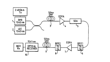
communications system. With reference to Figure 8, a DFB
laser 1 is used as the transmitter, directly modulated with
a 2.488~bit/s pseudo-random NRZ 2l5-1 pattern. The DFB laser
1 has a wavelength of As=1544.7nm. The bias and modulation
of the DFB 1 were chosen to give good extinction ratio but,
consequently, large chirp. The signal is combined at the
transmitter end of the system with CW light from a pump laser
2, a long external cavity (LEC) laser operating at
Ap=1543.lnm. The combined pump and signal is transmitted
across 50km normal-dispersion single-mode fibre 3, with a
dispersion of 17ps/nm.km at the signal wavelength. After
amplification by an Erbium-doped fibre amplifier 4 (EDFA),
the light was coupled into an SOA 5. The SOA is an etched-
mesa buried hetrostructure device with an active layer of
InGaAsP and both facets anti-reflection coated to less than
103 reflectivity. The SOA is operated at high injection
current (300mA), but the gain is saturated by the injected
light with less than ldB residual Fabry-Perot ripple. The
phase-conjugate signal is generated by NDFWM within the SOA,
with a wavelength given by lpC={21p-l-As-l~-l = 1541.4nm. An
optical bandpass filter 6 (1.3nm bandwidth) follows the SOA
and allows only the phase-conjugate signal to be transmitted.
This signal is amplified by a further EDFA 7 and further
filtered by filter 8 (0.6nm filter) then transmitted across
a second 50km length of single-mode fibre 9. The signal is
detected using a PIN-FET optical receiver 10.
Spectra at the output of the SOA are shown in Figure
9, (a) with and (b) without the signal beam. With the signal
WO95/~ PCT/GB94/00602
2i6S564 - 20 -
and pump both present and with polarisations aligned, the
phase-conjugate signal at 1541.4nm is generated, with the
inverted spectral profile of the DFB signal beam. The fibre
input powers of the pump and signal beams into the SOA are
+2.7dBm and -4.ldBm respectively. The background to the
spectra is from amplified spontaneous emission from both the
EDFA and the SOA and causes a reduction in the signal-to-
noise ratio. In order to maximise both the signal-to-noise
ratio and conversion efficiency the SOA is operated with high
gain and moderately high input optical power. Taking into
account the coupling loss into and out of the SOA, the
conversion efficiency of the phase conjugation (i.e. ratio of
the power of the phase conjugate beam at the output facet to
signal power coupled into the SOA) is +2.4dB, with a phase-
conjugate of -5.6dBm at the output facet of the SOA. This
conversion efficiency is at least 20dB greater than using
DSF, and can be further increased by using a SOA with higher
output power.
The effect of the dispersion compensation is clearly
seen by comparison of the eye diagrams of Figure 10, where
(a), (b) and (c) correspond to the back-to-back measurement,
and 10Okm transmission without and with dispersion
-compensation, respectively. The figures are all taken from
the receiver output with -26dBm received optical power. The
effects of fibre chromatic dispersion are evident from the
distortion of the eye diagram (b), but the clean eye is
completely recovered by the dispersion compensation (Figure
(c) ).
Bit error rate (BER) measurements were performed for
back-to-back transmission, and 100km transmission with and
without dispersion compensation, and the results are shown in
Figure 11. The back-to-back measurement, with the DFB signal
directly into the receiver, shows a sensitivity of -27.5dBm.
The inclusion of a 0.6nm bandpass filter results in a power
3S penalty of less than 0.ldB. Transmission of the DFB signal
over 100km without compensation (with a single EDFA at the
transmitter) results in a considerable dispersion penalty,
W095/03C~ PCT/GB941~602
- - 21 - ~ 5
and BERs as low as 109 could not be achieved. A similar eye
diagram and BER characteristic were obtained using the
arrangement of Figure 8, but with the filters tuned to
transmit the DFB signal. With dispersion compensation, a
dramatic improvement in the BER characteristic is seen, with
109 BER at -25.5dBm. The 2dB penalty results both from a
reduction in extinction ratio and the introduction of signal-
spontaneous beat noise, both arising from the introduction of
amplifier spontaneous emission.
Thus chromatic dispersion compensation using optical
phase conjugation in a semiconductor optical amplifier has
removed the dispersion penalty in the transmission of a
directly-modulated 2.5Gbit/s signal at 1.5~m over 100km of
normal dispersion fibre. The efficiency of the phase
conjugation is high at +2.4dB, despite the lack of cavity
enhancement.
In an alternative embodiment the SOA 5 is provided by
a DFB laser having a wavelength of 1543nm, thus allowing the
pump laser 2 to be dispensed with. In this embodiment the
20 pump radiation at 1543nm is generated within the SOA 5.
Again, in order to maximise the efficiency of phase
conjugation the SOA (in this case a DFB) is operated to
provide maximum output power, i.e. with a high injection
current, typically more than 10 times the threshold current.
Furthermore the average power of the optical signal injected
into the SOA 5 is limited to a level such that the degree of
gain modulation caused in the SOA is small, typically less
than ldB.