Note: Descriptions are shown in the official language in which they were submitted.
CA21 65596
OU ~ BUFFER CIRCUIT
- FOR HIGH-SPEED LOGIC OPERATION
BACKGROUND OF THE INVENTrON
1. Field of the Invention
The present invention relates to an output buffer
circuit and more particularly, to an output buffer circuit
applicable to high-speed logic operation using two
field-effect transistors (FETs~ serially connected to each
other, which is preferably realized on semiconductor
integrated circuits.
2. Description of the Prior Art
Fig. 1 shows a conventional output buffer circuit 31,
which has first and second n-channel enhancement
metal-oxide-semiconductor FETs (MOSFETs) 41 and 42 serially
connected to each other. The MOSFETs 41 and 42 are provided
between a positive supply terminal 44 and a negative supply
terminal 45 of the circuit 31.
A drain of the first MOSFET 41 is connected to the
positive supply terminal 44 and is applied with a positive
supply voltage +Vdd. A source of the first MOSFET 41 is
connected to a drain of the second MOSFET 42. A source of
the second MOSFET 42 is connected to the negative supply
terminal 45 and is applied with a negative supply voltage -
CA21 655'~6
-
v~
An output terminal 46 of the circuit 31 is connected
to the connection point of the source of the first MOSFET 41
and the drain of the second MOSFET 42. A digital output
signal Sc is taken out from the output terminal 46.
A gate of the first MOSFET 41 is directly connected
to an input terminal 32 outside the circuit 31. This gate is
applied with a first digital input signal Sa that is supplied
into the input terminal 32.
. 10 A gate of the second MOSFET 42 is connected to the
input terminal 32 through an inverter 34. A gate of the
second MOSFET 42 is connected to an output end of the
inverter 34. An input end of the inverter 34 is connected to
the input terminal 32. The gate of the second MOSFET 42 is
applied with a~ second digital input signal Sb. The second
input signal Sb is produced by inverting the logic state of
the first input signal Sa by the inverter 34.
The first input signal Sa is of a positive logic and
the second input signal Sb is of a negative logic. Therefore,
the second input signal Sb is always opposite in logic state
to the first input signal Sa.
When the first input signal Sa ls in the high or "H"
level, the second input signal Sb is in the low or "L"
level. Therefore, the first enhancement MOSFET 41 is ON or
CA21 655q6
... ~
conductive and the second enhancement MOSFET 42 is OFF or
nonconductive and as a result, the output signal Sc is in the
high or H level.
On the other hand, when the first input signal Sa is
in the L level, the second input signal Sb is in the H
level. Therefore, the first MOSFET 41 is OFF and the second
MOSFET 42 is ON and as a result, the output signal Sc is in
the L level.
Thus, if one of the first and second MOSFETs 41 and
42 is ON, the other thereof is always OFF, which means that
none of the MOSFETs 41 and 42 are ON simultaneously.
Accordingly, no current flows through the MOSFETs 41 and 42
in either steady state except for a leakage current of the
MOSFET 41 or 42, resulting in low power dissipation.
The conventional output buffer circuit 31 described
above has the following problem.
When the output signal Sc is turned from the L level
to the H level, in other words, the first input signal Sa is
turned from the L level to the H level, the first MOSFET 41
cannot be rapidly changed from the nonconductive state to the
conductive state. Consequently, the circuit 31 cannot respond
quickly to the rapid transition of the first input signal Sa
because the output signal Sc is delayed to rise with respect
to the first input signal Sa.
- CA21 65596
~ This problem is caused by the fact that the first
- MOSFET 41 needs to have the gate-to-source voltage VGS greater
than its threshold voltage VTH in order to be turned on. The
MOSFET 41 starts to be turned on after the delay in which
the gate-to-source voltage VGS increases from the ground to
the threshold voltage VTH and therefore, the output signal Sc
starts to rise after the same delay.
Sl1~ARY OF THE INVENTION
Accordingly, an object of the present invention is to
provide an output buffer circuit that enables to reduce the
delay of a digital output signal with respect to an input
digital signal.
Another object of the present invention is to provide
an output buffer circuit applicable to high-speed logic
operation.
Still another object of the present invention is to
provide an output buffer circuit that can provide a function
of limiting the swing of an output signal, thereby enhancing
the high-speed logic operation.
These objects together with others not specifically
mentioned will become clear to those skilled in the art from
the following description.
An output buffer circuit according to the present
CA21 655q6
~ invention includes first and second FETs serially connected
to each other. A gate of the first FET is applied with a
first digital input signal. A gate of the second FET is
applied with a second digital input signal. The first and
second FETs operate to be opposite or complementary in logic
state to each other. A digital output signal is taken out
from a connection point of the first and second FETs.
The circuit further includes a current source for
causing a bias current having the same direction or polarity
as that of a drain current of the first FET to flow through
the first FET in the pseudo-OFF state.
The "pseudo-OFF state" is defined as an OFF state
that is the same as the ordinary OFF state of the first FET
if the bias current does not flow through the first FET.
With the output buffer circuit according to the
present invention, when the first FET is in the pseudo-OFF
state, the bias current having the same direction or polarity
as that of a drain current of the first ~ET flows through
the first FET by the current source. Therefore, in the next
turn-on process, the drain current of the first FET starts to
increase from the value of the bias current to a specified
turn-on current value. This means that the first FET can be
turned on more quickly than the case in which no bias current
is supplied to the first FET in the ordinary OFF state.
CA2 1 655~6
~ As a result, the output buffer circuit according to
the present lnvention can reduce the delay of the output
signal with respect to the first input signal. This means
that the circuit according to the present invention can be
applied to high-speed logic operation.
Also, as the bias current is supplied to the first
FET in the pseudo-OFF state, the gate-to-source voltage of
the first FET is increased. Accordingly, the swing of the
output signal is reduced compared with the case in which no
current is supplied to the second FET in the OFF state.
The first and second FETs may be made of any FET;
however, they are preferably made of MOSFETs, because they
are readily formed on the large-scale integrated circuits
(LSIs).
Also, though the first and second FETs may be of an
enhancement or depletion type, the enhancement type is
preferred since the advantage of the invention can be
effectively obtained.
The conductivity type of the first and second FETs
may be the same as or different from each other if the first
and second input signals opposite in logic state to each
other are applied to the gates of the first and second FETs,
respectively.
The bias current may be set as any value if it has
- CA21 65596
- the same direction or polarity as that of a drain current of
the first FET. The maximum value of the bias current is
limited by the m~x;mllm current value that is allowed to flow
by the first FET in the pseudo-OFF state. However, if the
current value is far greater than the threshold current, the
power dissipation of this output buffer circuit becomes very
large. As a result, the bias current value is preferably set
as a value near the threshold current of the first FET. More
preferably, the bias current value is slightly greater than
the threshold current.
It is preferred that the bias current Ib is set as
any value in the range of ITH < Ib S lOOITH~ where ITH is the
threshold current of the first FET. In this case, both the
reduced signal delay and low power dissipation can be
performed.
It is more preferred that the bias current Ib is set
as any value in the range of 2ITH S Ib S 50ITH. In this case,
a margin for the threshold current fluctuation is given and
therefore, the effect of the signal delay reduction is
ensured to be accomplished even if the threshold current
fluctuation is caused by the variation of the fabrication
process conditions. Also, the power dissipation can be
restrained.
In a preferred embodiment, the current source is
~A2~ 6559~
composed of a third FET connected in parallel to the second
- FET and a voltage source for supplying a bias voltage to a
gate of the third FET. An additional advantage that the bias
current value can be readily adjusted by changing the bias
voltage value is obtained.
The voltage source is preferably made of a fourth FET
whose gate is connected to a gate of the third FET. The gate
and a drain of the fourth FET are connected to each other.
An additional advantage that the voltage source can be simply
configured is provided.
A fifth FET whose gate and drain are connected to
each other or a resistor may be additionally provided for the
voltage source. In this case, an advantage that the bias
voltage can be readily adjusted by changing the resistance of
the fifth FET or the resistor is provided.
In another preferred embodiment, the current source
is composed of a current mirror made of third and fourth
FETS. The third FET iS connected in parallel to the second
FET and produces the bias current. The fourth FET produces a
reference current. The bias current is proportional to the
reference current. An additional advantage that the bias
current is not affected by the threshold voltage fluctuation
is obtained. There is a further additional advantage that the
bias current is not affected by the threshold voltage
~i21 65~96
fluctuation and that the bias current can be determined by
- the gate-width to gate-length ratios of the third and fourth
FETs is obtained.
The output buffer circuit according to the invention
can be applied to various purposes other than the output
buffer circuit.
BRIEF DESCRIPTION OF THE DRAWINGS
In order that the invention may be readily carried
into effect, it will now be described with reference to the
accompanying drawings.
Fig. 1 is a circuit diagram of a conventional output
buffer circuit.
Fig. 2 is a circuit diagram of an output buffer
circuit according to a first embodiment of the invention.
Fig. 3 is a tlme chart showing a time response of the
output buffer circuit according to the first embodiment in
Fig. 2 and the conventional output buffer circuit of Fig. 1.
Fig. 4 is a circuit diagram of an output buffer
circuit according to a second embodiment of the invention.
Fig. 5 is a circuit diagram of an output buffer
circuit according to a third embodiment of the invention.
Fig. 6 is a circuit diagram of an output buffer
circuit according to a fourth embodiment of the invention.
r A~ 1 6 5596
Fig. 7 is a circuit diagram of an output buffer
circuit according to a fifth embodiment of the invention.
Fig. 8 is a diagram showing the ID_VGS characteristics
of an n-channel enhancement MOSFET operating in the
saturation region.
DETAILED DESCRIPTION OF THE PREFERRED EMBODIMENTS
Preferred embodiments of the present invention will
be described in detail below while referring to Figs. 2 to
8.
FIRST EMBODIMENT
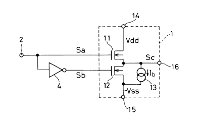
As shown in Fig. 2, an output buffer circuit
according to a first embodiment has a first n-channel
enhancement MOSFET 11 and a second n-channel enhancement
MO$FET 12 that~ are serially connected to each other. The
MOSFETs 11 and 12 are provided between a positive supply
term; n~ 1 14 and a negative supply terminaI of the circuit 1.
Specifically, a drain of the first MOSFET 11 is
connected to the positive supply term;n~l 14 and is applied
with a positive supply voltage +Vdd. A source of the first
MOSFET 11 is connected to a drain of the second MOSFET 12.
A source of the second MOSFET 12 is connected to the negative
supply terminal 15 and is applled with a negative supply
voltage -V~s.
--10--
C~21 65596
-
An output terminal 16 is connected to the connection
point of the source of the first MOSFET 11 and the drain of
the second MOSFET 12. A digital output signal Sc is taken out
from the output terminal 16.
A gate of the first MOSFET 11 is directly connected
to an input terminal 12 provided outside the buffer circuit
1. This gate is applied with a first digital input signal Sa
that is supplied into the input term; n~ 1 2 .
A gate of the second MOSFET 12 is connected to the
input term; n~l 12 through an inverter 4. A gate of the second
MOSFET 12 is connected to an output end of the inverter 4.
An input end of the inverter 4 is connected to the input
term; n~l 2 . The gate of the second MOSFET 12 is applied with
a second digital input signal Sb. The second input signal Sb
is produced by inverting the logic state of the first input
signal Sa by the inverter 4.
The first input signal Sa is of a positive loglc and
the second input signal Sb is of a negative logic. Therefore,
the second input signal Sb is always opposite or
20 complementary in logic state to the first input signal Sa.
In other words, the first and second FETs operate to be
opposite or complementary in logic state to each other.
When the first input signal Sa is in the H ~high)
level, the second input signal Sb is in the L (low) level.
~A2 1 65596
At this time, the first enhancement MOSFET 11 is ON or
conductive and the second enhancement MOSFET 12 is OFF or
nonconductive and as a result, the output signal Sc is in the
H level.
On the other hand, when the first input signal Sa is
in the L level, the second input signal Sb is in the H
level. At this time, the first MOSFET 11 is OFF and the
second MOSFET 12 is ON and as a result, the output signal Sc
is in the L level.
Thus, none of the first and second MOSFETs 11 and 12
is ON simultaneously and accordingly, no current flows
through the MOSFETs 11 and 12 in elther steady state except
for a leakage current of the MOSFET 11 or 12, resulting in
low power dissipation.
The above configuration is the same as that of the
conventional output buffer circuit 31 shown in Fig. 1.
Unlike the conventional circuit 31, the output buffer
circuit 1 of the invention has a constant current source 13
connected in parallel to the second MOSFET 12. One end of the
current source 13 is connected to the cQnnection point of the
drain of the second MOSFET 12 and the source of the first
MOSFET 11. The other end of the current source 13 is
connected to the source of the second MOSFET 12.
The current source 13 produces a constant current as
-12-
CA21 65596
a bias current Ib for the first MOSFET 11. The bias current
Ib has the same flowing direction or polarity as that of a
drain current of the first MOSFET 11.
When the first MOSFET 11 is in the ON state, that is,
the output signal Sc is in the H level, the bias current Ib
flows from the positive supply terminal 14 to the negative
supply terminal 15 through the first MOSFET 11 and the
current source 13.
The bias current Ib continues to flow through the
first MOSFET 11 even when the first MOSFET 11 is in the OFF
state, that is, the output signal Sc is in the L level. In
other words, the bias current Ib is extracted from the first
MOSFET 11 as a leakage current even if the MOSFET 11 is in
the OFF state. In the present invention, this state where the
bias current Ib flows through~the first MOSFET 11 in spite of
no drain current flowing therethrough is termed the "pseudo-
OFF" state.
Accordingly, in the next turn-on process of the first
MOSFET 11, the drain current starts to increase from the bias
current Ib, not from zero. This means that the first MOSFET
11 can turn on more quickly than the conventional circuit 31
in which no bias current is supplied to the first MOSFET 11
in the OFF state.
Consequently, the output buffer circuit 1 according
-13-
CA21 65596
.
to the first embodiment can reduce the delay time of rising
of the digital output signal Sc with respect to the first
input digital signal Sa. Therefore, the circuit 1 is
applicable to high-speed logic operation.
Also, as the bias current Ib flows through the first
MOSFET 11 even in the pseudo-OFF state, the swing of the
output signal Sc can be reduced compared with the
conventional circuit 31.
Next, the principles of the signal delay reduction
and the output swing reduction are explained in more detail
below.
Fig. 8 shows a typical transfer characteristic of an
n-channel enhancement MOSFET operating in the saturation
region for VDS > (VGS - VTH), where VDS~ VGS~ VTH and ID are a
drain-to-source voltage, a gate-to-source voltage, the
threshold voltage, and a drain current of the MOSFET,
respectively.
As seen from Fig. 8, the drain current ID starts to
gradually increase from zero (0) at a point A with the
increasing gate-to-source voltage VGS to the threshold current
ITH at a point B where VGS = VTH. The drain current ID then
increases linearly according to the square-root law in the
range from the point B to a point E where VGS = V3 and ID =
I3 as VGS increases. In the region where VGS > V3 or ID > I3,
CA2 1 65596
.~
although the drain current ID further increases, the increase
is not linearly.
The square-root law of the MOSFET is expressed as the
following equation (1):
ID K ( L ) ( VGS ~ VTh. )2 ( 1 )
where K is a constant, and L and W are the channel-length
and channel-width of the MOSFET, respectively.
In the output buffer circuit 1 according to the first
embodiment, the first MOSFET 11 operates at an operating
point D' where VGS = V2 ' and ID = I2' in the ON state, and it
operates at an operating point C where VGS = V1 and ID = I1
near the point B in the pseudo-OFF state due to the bias
current Ib. The voltage V1 is greater than the threshold
voltage VTH and less than the voltage V2', i.e. , VTH < V1 <
V2'. The current I1 is greater than the threshold current ITH
and less than the current I2', i.e. , IT~ < I1 < I2'. The
bias current Ib continues to flow through the first MOSFET 11
in the pseudo-OFF state, and therefore, I1 = Ib is
established.
As described above, in a turn-on process of the first
MOSFET 11, since the bias current Ib (= I1) that is slightly
`_ CA21 65596
greater than the threshold current ITH continues to flow
through the first MOSFET 11 in the pseudo-OFF state, the
drain current ID of the first MOSFET 11 starts to increase
from I1 and ends at I2' to be turned on. In other words, the
gate-to-source voltage VGS of the first MOSFET 11 starts to
increase from V1 and ends at V2' to be turned on.
On the other hand, with the conventional output
buffer circuit 31, since no bias current flows through the
first MOSFET 41, the first MOSF~T 41 operates at an operating
point D where VGS = V2 (< V2 ~ ) and ID = I2 (< I2') in the ON
state, and it operates at an operating point A where VGS =
and ID = O in the OFF state.
In a turn-on process of the first MOSFET 41, since no
bias current flows through the first MOSFET 41 in the OFF
state, the drain current ID of the first MOSFET 41 starts to
increase from zero and ends at I2 to be turned on. In other
words, .the gate-to-source voltage VGS of the first MOSFET 41
starts to increase from zero and ends at V2 to be turned on.
Thus, the circuit 1 according to the first embodiment
has a shorter turn-on time of the first MOSFET 11 than the
conventional circuit 31. In other words, the first MOSFET 11
of the circuit 1 can be turned on more quickly than that of
the conventional circuit 31. Accordingly, the delay of the
rising of the output signal Sc can be decreased.
-16-
CA21 65596
. ,.
Fig. 3 shows a time response of the output buffer
circuit 1 according to the first embodiment and the
conventional output buffer circuit 31.
As shown in Fig. 3, when the first input signal Sa
S starts to rise at to, the output signal Sc starts to rise
approximately simultaneously with the first input signal Sa
in the circuit 1 according to the first embodiment.
Therefore, the output signal Sc starts to rise after
substantially no delay time with respect to the rise of the
first input signal Sa. The increase of the output signal Sc
ends at t2.
In contrast, the output signal Sc starts to -rise at
tl in the conventional circuit 31, which means that it starts
to rise after a delay time (tl - to) with respect to the rise
of the first input signal Sa The increase of the output
signal Sc ends at t3 that is later than t2.
Thus, the output signal Sc has substantially no delay
for the circuit 1 of the invention, and it has a delay of (t
- to) (~ 0) for the conventional circuit 31.
Next, the principle of the voltage swing of the
output signal Sc is explained.
As shown in Fig. 3, the output signal Sc has a high
voltage level VOH~ a low voltage level VOL, and a voltage
swing avO~ (= VOH - VOL). The voltage swing ~VO~ for the
CA21 6~9b
circuit 1 of the first embodiment is smaller than that for
the conventional circuit 31.
In the circuit 1, the bias current Ib continues to
flow through the first MOSFET 11 in the OFF state, and
therefore, the gate-to-source voltage VGS of the first MOSFET
11 becomes higher compared with the case where no bias
current is supplied. As a result, the high voltage level VOH
of the output signal Sc decreases by a voltage corresponding
to the reduct on of VGS. This means that the circuit 1 of the
first embodiment has a functlon of limiting or reducing the
voltage swing ~VOUT for the output signal Sc.
This voltage-swing reducing function for the output
signal Sc enhances the turn-on speed of the first MOSFET 11,
the reason of which is as follows: ~
In general, the operation speed of a logic circuit
varies dependent upon the logic swing and the rise/fall time
of the output signal Sc. When the signal Sc has a constant
rising slope of the waveform, the response time of the signal
Sc is proportional to its logic swing. Consequently, the
rising/falling time is improved due to the voltage-swing
reducing function.
The inventor performed a simulation under the
condition that W = 200 ~m, L = 0.35 ~m, ITH = 1 ~A, and Ib
= 50 ~A. The simulation results stated that the rise time (=
-18-
CA21 65596
-
t3 - t1) of the output signal Sc for the conventional circuit
31 was 25 ns or longer, and that the rise time (= t2 - to)
for the circuit 1 of the first embodiment was 1.9 ns. It is
clearly seen from the results that the circuit 1 has the
highly decreased rise time of the output signal Sc compared
with the conventional circuit 31, and that the operation
speed of the circuit 1 is highly improved.
SECOND EMBODIMENT
As shown in Fig. 4, an output buffer circuit la
according to a second embodiment is the same in configuration
as that of the first embodiment except that a third n-channel
enhancement MOSFET 21 and a voltage source 22 are provided
instead of the constant current source 13. Therefore, the
description about the same configuration is omitted here by
attaching the same reference numerals to the corresponding
elements for the sake of simplification of description.
The third MOSFET 21 is connected in parallel to the
second MOSFET 12. Specifically, the MOSFET 21 has a drain and
a source connected to the drain and source of the MOSFET 12,
respectively. One end of the voltage source 22 is connected
to the gate of the third MOSFET 21 and the other end is
grounded. The voltage source 22 supplies a positive constant
voltage to a gate of the MOSFET 21 as a bias voltage Vb.
The third MOSFET 21 produces a drain current ID
-19-
CA21 65596
proportional to the applied bias voltage Vb. If the bias
voltage Vb is set to satisfy the equation of ID = Ib, the
same bias current Ib as in the first embodiment is supplied
to the first MOSFET 11 in the OFF state. Therefore, the same
effects or advantages can be obtained in the second
embodiment.
Also, an additional advantage that the bias current
Ib for the first MOSFET 11 can be readily adjusted by
changing the constant bias voltage Vb of the voltage source
22.
There is a further advantage that the bias current is
not affected by the threshold voltage (or current)
fluctuation caused during the fabrication process sequence,
because the threshold voltage fluctuation is cancelled by the
fluctuation of the bias current Ib.
- THIRD EMBODIMENT
Fig. 5 shows an output buffer circuit lb according to
a third embodiment, which is the same in configuration as
that of the second embodiment except that a fourth n-channel
MOSFET 23 and a fifth n-channel MOSFET 24 are provided as the
voltage source 22 in the second embodiment. Therefore, only
the description about the different configuration is shown
here for the sake of simplification of description.
The fourth MOSFET 23 whose gate and drain are coupled
-20-
CA21 65596
._
together and the fifth MOSFET 24 whose gate and drain arecoupled together are serially connected to each other.
The gate and drain of the fourth MOSFET 23 is
connected to the gate of the third MOSFET 21. A source of
the MOSFET 23 is applied with the negative supply voltage -
V~. A source of the fifth MOSFET 24 is connected to the
drain and gate of the third MOSFET 23. The drain and gate of
the fifth MOSFET 24 are applied with the positive supply
voltage +Vdd. The two MOSFETs 23 and 24 have the sa~.e size.
The bias voltage Vb produced by the fourth and fifth
MOSFETs 23 and 24 is defined by the resistances of the two
MOSFETs 23 and 24. The bias current Ib is defined
corresponding to the ratio of the gate-width to gate-length
ratios of the third and fourth MOSFETs 21 and 23. That is,
if the third and fourth MOSFETs 21 and 23 have the channel-
width to channel-length ratios (W/L) 21 and (W/L) 23~
respectively, the bias current Ib is expressed by the
following equation (2).
(--)21
L ~ ( 2)
( L )23
where Ir is a reference current produced by the fourth and
-21-
~ CA21 65596
fifth MOSFETs 23 and 24.
Since the third and fourth MOSFETs 21 and 23 have the
channel-width to channel-length ratios (W/L)zl and (W/L) 23 that
are equal to each other in the third embodiment for a
simplified explanation, the reference current Ir is equal to
the bias current Ib and is be expressed by the following
equation (3).
, Ib K (L)2l( - - VTq)2 (3)
If the threshold voltage VTH becomes higher or lower,
the bias current Ib increases or decreases corresponding to
the change of the voltage VTH. Accordingly, the ratio of the
threshold current ITH and the bias current Ib does not change.
The same effects or advantages as those in the second
embodiment can be obtained in this third embodiment.
It can be said that The third, fourth and fifth
MOSFETs 21, 23 and 24 constitute a current mirror circuit, in
which the reference current Ir is defined by the MOSFETs 23
and 24 and the bias current Ib is defined by a mirror
current.
FOURTH EMBODIMENT
Fig. 6 shows an output buffer circuit lc according to
a fourth embodiment, which is the~ same in configuration as
that of the third embodiment except that a resistor 25 is
provided instead of the fourth MOSFET 25 in the third
embodiment.
One end of the resistor 25 is appliced with the
positive supply voltage Vdd and the other end is connected to
the coupled drain and gate of the fourth MOSFET 23.
The operation of the circuit lc of the fourth
embodiment is substantially the same as the circuit lb of the
third embodiment.
If the resistance of the resistor 25 is very high
such as 1 MQ, the bias voltage Vb is approximately equal to
the threshold voltage VTH, i.e . , Vb ~ VTH. Therefore, when
the first, third and fourth MOSFETs 11, 21 and 23 have the
same channel-width to channel-length ratio, the operating
point of the first MOSFET 11 is set at the point B. If the
third MOSFET 21 has the dhannel-width to channel-length ratio
twice as much as that of the fourth MOSFET 23, the operating
point of the first MOSFET 11 is set at a point where Vb is
2 VTH or Ib is 2 ITH-
Thus, in the fourth embodiment, the operating pointof the first MOSFET 11 can be set by adjusting the ratio of
the channel-width to channel-length ratios tW/L) of the third
and fourth MOSFETs 21 and 23.
CA2 1 655~b
- FIFTH EMBODIMENT
Fig. 7 shows an output buffer circuit ld according to
a fifth embodiment, which is the same in configuration as
that of the first embodiment except that a p-channel
enhancement MOSFET lla is provided instead of the first
MOSFET 11 and the inverter 4 is omitted. Therefore, the
circuit ld has the complementary MOS (CMOS) configuration.
One end of the resistor 25 is applied with the
positive supply voltage Vdd and the other end is connected to
the coupled drain and gate of the fourth MOSFET 23.
The operation of the circuit ld of the fifth
embodiment is substanti-ally the same as the circuit 1 of the
first embodiment, and therefore, the same effects or
advantages can be obtained.
The output buffer circuits according to the first to
fifth embodiments have two supply terminals 14 and 15 that
are applied with the positive and negative supply voltages Vdd
and V~c, respectively. However, one of the terminals 14 and
15 may be grounded. In this case, the voltage swing of the
output signal Sc is reduced.
In the above first to fourth embodiments, n-channel
MOSFETs are employed. However, it is needless to say that
p-channel MOSFETs may be employed.
While the preferred forms of the present invention
-24-
CA~ 1 6~59~
have been described, it is to be understood that
modifications will be apparent to those skilled in the art
without departing from the spirit of the invention. The
scope of the invention, therefore, is to be determined solely
by the following claims.
-25-