Note: Descriptions are shown in the official language in which they were submitted.
216562
-1-
BERESKIN & PARR
File 8305-005
Title:
POWER FACTOR CORRECTION CIRCUTTRY
FIELD OF THE INVENTION
This invention relates to power factor correction circuits, and
more particularly to power factor correction circuits for switch mode
power supplies and electronic ballasts.
BACKGROUND OF THE INVENTION
The demand and development of power factor correction
circuitry has been fuelled by concern over the massive use of electronic
power conversion, i.e. AC to DC power supplies, and the resulting
potential for contamination of AC power lines.
Power factor is defined as the ratio of the actual power (Watts)
developed by an AC power system to the apparent power (i.e. volt-
amperes).
Most electronic ballast and switching power supplies use a
bridge rectifier and a bulk storage capacitor to derive raw DC voltage
from the AC power line. Such a circuit draws power from the AC line
when the instantaneous AC voltage exceeds the capacitor voltage. This
occurs near the line voltage peak and results in a high charge current
spike. Since power is only taken near the line voltage peaks, the
resulting spikes of current are extremely non-sinusoidal and have a
high harmonic content. The result is a power supply with a poor
power factor where the apparent input power is much higher than the
2165623
-2-
real power. The power factor (i.e. ratio of actual power developed to the
apparent power) is typically in the range 0.5 to 0.?. In response,
International Standards are being established to control this type of
harmonic loading on power systems, for example, IEC Standard 555.2
defines the maximum levels of harmonic content a device can draw
from an AC power line.
To achieve a high power factor, e.g. in the range of 0.99, the
current which is drawn should have a sinusoidal wave shape and the
sinusoidal current should not be more than a few degrees out of phase
with the sinusoidal waveform for an AC voltage supply. Power factor
correction circuits according to the art fall into two broad groups:
passive and active. The passive power factor correction circuits usually
contain a combination of large capacitors, inductors and rectifiers that
operate at the frequency of the AC power line to provide a resonant
circuit which produces a sinusoidal current waveform. While passive
power factor correction circuits can produce a high power factor, they
are not very efficient. Active power factor correction circuits, on the
other hand, incorporate some form of high frequency switching
converter for power processing of the voltage and current waveforms.
They typically utilize microchip technology to control operation of the
power supply circuit and produce a current waveform with a
sinusoidal shape. A popular topology is the "boost converter" which
will be familiar to those skilled the art. Since active power factor
circuits operate at a frequency which is much higher than the AC
power line, the circuits can be smaller, lighter in weight, and more
efficient than a passive circuit.
While known power factor correction circuits have provided
elegant solutions to the problem of power factor control by keeping the
current drawn from the AC power line sinusoidal and "in-phase" with
the line voltage, known power correction circuits still possess less than
ideal characteristics. One shortcoming common to most power factor
correction circuits is the presence of a current path in the switch-off
21b5~23
-3-
state which in practical terms means that the load will be "live" or
connected to the full wave rectified AC voltage requiring care and
caution for testing and maintenance operations, e.g. the use of isolation
transformers. This problem has been addressed in the prior art by
including elaborate protection circuitry for the output stage. Another
problem associated with known power factor correction circuits arises
from the requirement that the voltage on the bulk capacitor must be
greater than the input line voltage, i.e. V~pp >_ 1.2 ~2 VI~UT to provide
the capability to maintain a sinusoidal wave-shape for the current. In
practical terms, this makes it next to impossible to provide a compact
electronic ballast system for a high voltage application, e.g. > 347 volts.
Another shortcoming of known power factor correction systems
concerns the bulk capacitor. Because there is an off-state current or
charge path, the bulk capacitor must be able to handle the voltage 1.2 ~2
vINPUT~ which means that the capacitor will have a fairly high value,
i.e. in micro-Farad range. Capacitors in this range are typically large in
size and comprise electrolytic dielectrics. The large size of the capacitor
limits the output capacity of the power supply and also makes it
difficult to miniaturize the power circuit, and therefore applications
such as laptop and notebook computers and line powered personal
digital assistants (PDA's) are limited. Furthermore, it is not desirable to
use electrolytic capacitors because of their unreliable nature as will be
understood by those skilled in the art. For example, electrolytic
capacitors, and specifically the dielectric layer, are prone to breakdown
over time and susceptible to environmental factors such as humidity
and heat.
The maximum performance for power supplies using
existing power factor correction circuitry (i.e. electrolytic capacitors) is
typically 30 Watts/in3. This makes it impractical to use such power
supplies, e.g. switching power supplies, for applications such as laptop
computers, or other electronic devices where size and weight are
important.
~ ~~6 ~3
-4-
Furthermore, the maximum power levels for known power
factor correction circuits are typically in the range 400 Watts, which as
will be understood by one skilled in the art makes these circuits
unsuitable for high voltage or high power applications, for example,
electronic ballast supplies for High Intensity Discharge ("HID") lamps.
Electronic ballast circuits are power supplies which are
designed for fluorescent, high intensity discharge, halogen, etc.. lighting
systems. The application of known power factor correction circuits, e.g.
boost converters, to electronic ballast circuits is limited because of the
requirements for a high output voltage or "start voltage" to initiate the
discharge and then a low output voltage or "running voltage" to
maintain the discharge.
Accordingly, there is a need for power factor correction
circuits which overcome the shortcomings of PFC circuits known in
the art.
BRIEF SUMMARY OF THE INVENTION
In a first aspect, the present invention provides a power factor
correction circuit for use with a power supply having an input port for
receiving an AC input signal and a rectifier for producing a rectified AC
signal and an output stage for outputting a DC output signal for driving
a load coupled to the output stage, said power factor correction circuit
comprising: (a) an input coupled to the rectifier for receiving the
rectified AC signal; (b) inductive means coupled to said input for
storing energy in response to excitation by the rectified AC signal; (c)
controller means for controlling excitation of said inductive means; (d)
charge storage means coupled to said inductive means for charging by
said inductive means under control of said controller means to
produce the DC output signal; and (e) blocking means which blocks a
direct path for current flow from said input to the load.
In a second aspect, the present invention provides a power
factor correction circuit for use with a power supply having an input
..-'
rw
vI>~..x -: ~ _
s~s~
-5-
port for receiving an AC input signal and a rectifier for producing a
rectified AC signal and an output stage for outputting a DC output
signal for driving a load coupled to the output stage, said power factor
correction circuit comprising: (a) an input coupled to the rectifier for
receiving the rectified AC signal; (b) charge storage means having first
and second terminals, the first terminal being connected to said input
and said connection forming a first output terminal and said second
terminal forming a second output terminal for connecting the load; (c)
inductive means for storing energy in response to excitation by the
rectified AC signal, said inductive means having first and second
terminals, the first terminal of said inductive means being connected to
said second output terminal; (d) means for isolating said inductive
means from said input port, said means for isolating being connected to
said input and to the second terminal of said inductive means; and (e)
controller means coupled to the second terminal of said inductive
means for controlling excitation of said inductive means by providing a
controllable current path through the load for the rectified AC signal to
excite said inductive means and the load providing means for damping
the rectified AC signal fed to said inductive means.
In a third aspect, the present invention provides a power
factor correction circuit for use with a power supply having a supply
input port for receiving an AC input signal and a rectifier for producing
a rectified AC signal and an output stage for outputting a DC output
signal for driving a load coupled to the output stage, said power factor
correction circuit comprising: (a) an input coupled to the rectifier for
receiving the rectified AC signal; (b) a booster stage coupled to said
input and having a booster output port and means for producing a
boosted signal from the rectified AC signal at said booster output port,
said booster stage further having means which blocks a direct path for
current flow from said input to said booster output; (c) a reducer stage
coupled to said booster output port and having means for generating
the DC output signal from said boosted signal; (d) controller means
a,~ ~ ~:
-
coupled to said booster stage and to said reducer stage for controlling
operation of said booster and reducer stages; and (e) said controller
means including means for increasing the power factor of the power
supply.
In an another aspect, the present invention provides a power
factor correction circuit for use with a power supply having an input
port for receiving an AC signal and a rectifier for producing a rectified
AC signal and an output stage for outputting a DC output signal for
driving a load coupled to the output stage, said power factor correction
circuit comprising: (a) an input having first and second terminals
coupled to the rectifier for receiving the rectified AC signal; (b)
inductive means for storing energy in response to excitation by the
rectified AC signal, said inductive means being coupled through a first
path to one of said terminals and through a second path to the other of
said terminals; (c) controller means for controlling excitation of said
inductive means, said controller means comprising a controller and a
switch, and said switch having a control input coupled to said
controller, said switch being operable in a conduction state and a non-
conduction state; (d) said switch being coupled in one of said first and
second paths between said inductive means and said input; (e) charge
storage means coupled to said inductive means for charging by said
inductive means under control of said controller means to produce the
DC output signal; so that when said switch is operating in said non-
conduction state, said one path is open.
BRIEF DESCRIPTION OF THE DRAWINGS
For a better understanding of the present invention, and to
show more clearly how it may be carried into effect, reference will now
be made, by way of example, to preferred embodiments of the present
invention shown the accompanying drawings in which:
Figure 1 shows in diagrammatic form a power factor
correction circuit according to the prior art;
rz
~~~~3
-6A-
Figure 2(a) shows in diagrammatic form voltage and current
waveforms for a prior art circuit which does not have power factor
correction;
Figure 2(b) shows in diagrammatic form voltage and current
waveforms for the known power factor correction circuit of Figure 1;
Figure 3 shows in diagrammatic form a power factor
correction circuit according to the present invention;
z ~:
a::~.w -- S J
265623
_...,
Figure 4 shows in diagrammatic form a second embodiment
of the power factor correction circuit according to the present
invention;
Figure 5 shows in diagrammatic form a third embodiment of
the power factor correction circuit according to the present invention;
Figure 6 shows in diagrammatic form a fourth embodiment
of the power factor correction circuit according to the present
invention; and
Figure 7 shows in diagrammatic form a fifth embodiment of
the power factor correction circuit according to the present invention.
DETAILED DESCRIPTION OF THE PREFERRED EMBODIMENTS
Reference is first made to Figure 1 which shows in
diagrammatic form a power factor correction circuit according to the
prior art. In Figure 1, the power factor correction circuit or PFC circuit is
denoted by reference 10. The PFC circuit 10 is part of an "off-line" power
supply circuit indicated generally by reference 12. The power supply 12
converts an AC voltage signal 14 from supply mains 15 into a DC
voltage signal 16.
As shown in Figure 1, the power supply 12 has an input 18
which couples the AC voltage signal 14 (and the supply mains 15) to a
full-wave rectifier 20. The output of the full-wave rectifier 20, i.e.
rectified AC voltage signal 14', is coupled to a capacitor 22. The function
of the capacitor 22 is to provide a DC offset to the rectified AC signal 14',
thereby keeping the rectified AC signal 14' above zero. The PFC circuit
12 is coupled between the capacitor 22 and an output or "bulk" capacitor
24. The output capacitor 24 for typical applications comprises a large
electrolytic capacitor, typically in the micro-Farad range and up. The
output capacitor 24 produces the constant DC voltage output signal 16
at an output port 26. The output port 26 couples to a load 28.
The PFC circuit 10 comprises an inductor 30, a power switch
32, a switch or diode 34 and a controller 36. One terminal of the
2165623
_8-
inductor 30 connects to the capacitor 22 and the other terminal of the
inductor 30 connects to the switch 32. The inductor 30 also connects to
the anode of the diode 34. As shown in Figure l, the power switch 32
has a control terminal 38 which is coupled to the controller 36. The
controller 36 uses the terminal 38 to control the state of the switch 32,
i.e. on or off. When the switch 32 is on, the inductor 30 stores energy
and when the switch 32 is off, the energy in the inductor 30 discharges
into the load 28 through the diode 34. During the discharge period, the
voltage across the inductor 30 adds to the voltage on the output
10 capacitor 24. The capacitor 24 also smooths the output voltage signal 16
to provide a constant DC output. According to the art, the controller 38
produces a pulse width modulated (PWM) signal 40 which controls the
switch 32 via the terminal 38 so that a charging current (i.e. inductor
current) having an average value which is sinusoidal in shape is
15 produced for charging the bulk capacitor 24. It is well-known that
shaping the charging current 17 (shown in Figure 2(b)) as a sinusoidal
signal which is not more than a few degrees out of phase with the
sinusoidal voltage signal 14 results in a power factor which approaches
unity, i.e. 0.99. The charging or inductor current 17 and the PWM
20 control signal 40 are shown in detail in Figure 2(b).
The controller 38 can comprise any one of a number of
commercially available microchips, such as the Motorola MC34262
power factor controller, the LT1249 power factor controller from Linear
Technology, or the HV-2405E power factor controller available from
25 Harris Semiconductor Corporation. The implementation of the
controller 38 is within the understanding of one skilled in the art.
Referring still to Figure 1, the switch 34 in the PFC circuit 10
typically comprises a diode. The diode 34 acts as a uni-directional
switch. When the diode 34 is forward biased (and the switch 32 is open),
30 the inductor current 17 will charge the capacitor 24 to an output voltage
level. The diode 34, however, prevents the capacitor 24 from
discharging through the switch 32 (if closed) or through the inductor
~1~~~~~
-9-
30. This allows the capacitor 24 to be charged or "boosted" to a value
which is higher than the AC input voltage 14.
Reference is next made to Figure 2(a) which shows the effect
if the power factor is uncorrected. As shown in Figure 2(a), the AC
input voltage signal 14 is a sinusoidal signal and the DC output voltage
16 is a relatively constant signal with some rippling. In response to the
charging of the output capacitor 24, an AC input line current 19 is
drawn by the power supply 12 from the supply mains 15. As shown in
Figure 2(a), the AC input line current 19 is highly non-sinusoidal and
comprises a series of pulses. The pulses in the AC input line current 19
coincide with the positive and negative peaks in the AC input voltage
14 and represent high charge current spikes which can cause the AC
line voltage 14 to "sag" as indicated by reference 21. Because of the
highly non-sinusoidal nature of the line current 19, the power factor
for uncorrected power supply is typically low and in the range 0.58 to
0.62.
Reference is again made to Figure 2(b) which shows the
inductor or charging current 17 which is produced by the power factor
correction circuit 10 as shown in Figure 1. When the power switch 32 is
ON, i.e. the PWM signal 40 is high, the inductor 30 is charged as
indicated by inductor current 17a. Conversely, when the power switch
32 is OFF, i.e. the PWM signal 40 is low, the inductor 30 discharges
through the diode 34 (current 17b) thereby charging the capacitor 24. By
using the switch 32 to control the charging and discharging of the
inductor 30, the shape of the inductor current 17 can be controlled. As
shown in Figure 2(b), the inductor current 17 has an average value 23
which is sinusoidal in shape and as described above leads to high
power factor.
It will be appreciated that the PFC circuit 10 according to the
prior art has three primary shortcomings. First, there is a direct path
between the rectified AC signal 14' and the load 28 when the switch 32
is open. Secondly, whenever the voltage on the capacitor 24 is less than
21~~~~
-lo-
the rectified AC signal 14', the capacitor 24 will charge. This means that
the capacitor 24 must have the capacity to handle the rectified AC
voltage 14' which is typically a high voltage. Thirdly, the high capacity
required for the capacitor 24 means that an electrolytic capacitor must
be used which can in turn affect the reliability and size of the PFC
circuit 10.
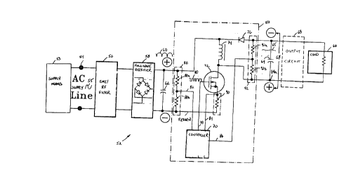
Reference is next made to Figure 3 which shows a power
factor correction (PFC) circuit 50 and power supply circuit 52 according
to the present invention. The power supply circuit 52 comprises an
input port 54, an EMI/RF filter stage 56, a full-wave rectifier 58 and the
power factor correction circuit 50. The input port 54 provides the input
for an AC supply signal 55 which is supplied by AC supply mains 53.
The EMI/RF filter stage 56 serves to isolate the power supply 52 from
high frequency noise, e.g. electromagnetic interference, which can
appear on the AC supply signal 55 and the supply mains 53. The full-
wave rectifier 58 comprises a known circuit configuration which can be
formed from four diodes. The function of the rectifier stage 58 is to
rectify the AC supply signal 55 to produce a rectified AC signal 60
comprising a series of positive pulses as shown in Figure 3. The output
of the rectifier 58 is connected to a capacitor 62 which produces a DC
offset to raise the zero crossing voltage thereby preventing the rectified
AC voltage 60 from going below zero. The capacitor 62 can comprise a
film capacitor and capacitance value as will be within the knowledge of
one skilled in the art. The power supply 52 also includes an output
capacitor 64 which is coupled to the PFC circuit 50. As will be described
below, a feature of the invention is that the output capacitor 64 can
have a much lower value (and smaller size) than the bulk capacitor 24
in known PFC circuits such as the circuit 10 shown in Figure 1.
As shown in Figure 3, a load 66 can directly connect to the
capacitor 64. The power supply 52 can also include an output circuit 68
(shown in broken outline) which is coupled between the capacitor 64
and the load 66. The output circuit 68 can comprise an inverter or a
2165623
-11-
high frequency driver or other known circuit elements as will be
within the understanding of one skilled in the art.
As shown in Figure 3, the PFC circuit 50 according to the
invention comprises a controller 70, a controllable switch 72, an
inductor 74 and a uni-directional switch or diode 76. The first terminal
of the inductor 74 provides the input to the PFC circuit 50 and is
connected to the output of the full-wave rectifier 58 and also to one
terminal of the capacitor 62. The first terminal of the inductor 74 is also
connected to the cathode of the diode 76. The anode of the diode 76 is
connected to the first terminal of the output capacitor 64 and also to the
load 66. The other terminal of the inductor 74 is connected to the input
of the switch 72 and also to the second terminal of the output capacitor
64. As shown in Figure 3, one of the features of the PFC 50 according to
the present invention is that the diode 76 is connected so that it
provides a "blocking" function by having a polarity which is opposite
to known PFC circuits 10 such as shown in Figure 1. This leads to a
number of advantages as will be described below.
Referring still to Figure 3, the switch 72 can be implemented
using, for example, a MOSFET transistor having a "gate" which is
connected to a control output 78 on the controller 70 and a "source"
connected to the second terminal of the inductor 74. The MOSFET
switch 72 also has a "drain" terminal and the connection of the drain is
described below. The controller 70 controls the state of the MOSFET
switch 72 through the gate by generating a pulse width modulated
(PWM) signal 80 on the control output 78. The controller 70 can be
implemented using known PFC devices, such as the Motorola MC34262
as will be within the understanding of one skilled in the art, and the
specification sheets for the MC34262 and MC33262 Family of Power
Factor Controllers are incorporated herein by this reference.
As shown in Figure 3, the controller 70 also includes three
sensing inputs denoted by references 82,84,86, respectively. The first
sensing input 82 is coupled to a voltage divider 88 which is formed
2165623
-12-
from two resistors 88a,88b that are connected across the capacitor 62.
The controller 70 uses the voltage divider 88 to monitor the voltage on
the capacitor 62 which also corresponds to the input voltage level (i.e.
rectified AC signal 60) for the PFC circuit 50. The second sensing input
84 is coupled to a resistor 90 which is connected between the drain of
the MOSFET switch 72 and RETURN or NEGATIVE terminal for the
supply mains 53. The controller 70 can determine the current flowing
in the switch 72 by reading the voltage drop across the resistor 90. The
third sensor input 86 is coupled to another voltage divider 92 which is
formed from two resistors 92a,92b and connected across the output
capacitor 64. The controller 70 uses the voltage divider 92 to monitor
the voltage across the output capacitor 64, i.e. the DC output voltage 65.
In operation, when the controller 78 closes the MOSFET
switch 72 (using the control output 78 connected to the gate of the
MOSFET), the circuit loop is completed and the rectified AC voltage 60
will induce a current to flow causing energy to be stored in the inductor
74. When the controller 78 opens the switch 72, the circuit loop is
opened. The inductor 74 appears as a high impedance to the rectified
AC signal 60 and the energy stored in the inductor 74 will discharge
into the capacitor 64. Because of its polarity, the diode 76 blocks the
flow of positive current through it and instead the energy stored in the
inductor 74 will discharge into the second terminal 64a of the capacitor
64 thereby charging the second terminal positively with respect to the
first terminal. Due to the operation of the diode 76, the polarity of the
output voltage (indicated by reference 67) is reversed from the polarity
of the AC supply signal 55. The polarity of the output voltage 67 seen by
the load 66 can be changed by including an inverter (not shown) in the
output circuit 68.
A feature of the PFC circuit 50 shown in Figure 3 is the
elimination of a direct charge path (or "off-state" current) through the
diode 76 when the switch 72 is open (i.e. OFF). When the MOSFET
switch 72 is open, there is no return path for the rectified AC signal 60
-13-
and the diode 76 blocks the rectified AC signal 60 from the load 66. The
advantages of this feature are first, isolation of the load 66 from the
rectified AC signal 60. Because the rectified AC signal 60 is typically a
high voltage signal, e.g. a 120, 220, 240, 277 or 347 Volts AC or VAC
signal which has been rectified, isolation of the load 66 is desirable for
safety reasons. The resultant isolation also eliminates the need for
elaborate protection circuitry as necessary in prior art devices. Secondly,
eliminating the off-state current means that the size of the capacitor 64
for the circuit 52 shown in Figure 3 is smaller because when the switch
72 is open, the capacitor 64 will not charge to the level of the rectified
AC voltage 60 (due to the blocking action of the diode 76). Unlike prior
art devices (e.g. Figure 1), the capacitor 64 in Figure 3 does not need to
handle a voltage, V~AP ? 1.2 ~2 VIN. In practical terms, this means that
the power supply 52 and PFC 50 shown in Figure 3 can be compact and
smaller in size than found in a conventional PFC circuit 12 shown in
Figure 1, and therefore the PFC circuit 50 according to the invention
can have wider application. As will be described below, the size of the
output capacitor 64 can be further reduced for other topologies
according to the present invention leading to further advantages in
terms of size and performance.
Reference is next made to Figure 4 which shows another
embodiment of a power factor correction circuit 50-1 and power supply
circuit 52-1 according to the present invention. As shown in Figure 4,
the power supply circuit 50-1 comprises an input port 54-1 (for
receiving an AC voltage signal 55-1 from the supply mains 53 (not
shown)), an EMI/RF filter stage 56-1, a full-wave rectifier 58-1 and the
PFC 50-1. The power supply circuit 52-1 shown in Figure 4 includes an
output circuit 68-1 which can comprise known circuits, for example, an
inverter or high frequency converter. The output circuit 68-1 is coupled
between an output capacitor 64-1 and load 66-1 as shown.
The PFC 50-1 shown in Figure 4 comprises a controller 70-1, a
switch 72-1, an inductor 74-1 and a diode 76-1. The controller 70-1 has a
2165523
-14-
control output 78-1 which is connected to the control input of the
switch 72-1. As described above for Figure 3, the controller 70-1 uses the
output 78-1 to control the state (i.e. OPEN or CLOSED) of the switch 72-1
by generating a pulse width modulated signal 80-1. The switch 72-1 can
be implemented as a MOSFET. It is a feature of the PFC 50-1 shown in
Figure 4 that the MOSFET switch 72-1 can be either a P-type or an N-
type. As shown in Figure 4, the source of the MOSFET switch 72-1 is
connected to the output of the full-wave rectifier 58-1 and receives
rectified AC voltage 60-1. The source of the MOSFET switch 72-1 is also
connected to the voltage divider 88-1 formed from resistors 88a-1,88b-1.
The controller 70-1 uses input 82-1 to sense the voltage level generated
by the divider 88-1 which corresponds to the voltage level of the
rectified AC signal 60-1. The drain of the MOSFET switch 72-1 is
connected to one terminal of the inductor 74-1 and also to the cathode
of the diode 76-1. The anode of the diode 76-1 is connected to one
terminal of the output capacitor 64-1 and the voltage divider 92-1. The
other terminal of the capacitor 64-1 is connected to the inductor 74-1
through the resistor 90-1.
In operation, when the switch 72-1 is closed by the controller
70-1 (through output line 78-1 and control signal 80-1), the rectified AC
voltage 60-1 will cause a current to flow in the inductor 74-1. Because
the inductor 74-1 appears as a high impedance to the rectified AC signal
60-1, energy will be stored in the inductor 74-1. When the controller 70
1 opens the switch 72-1, the energy stored in the inductor 74-1 will
discharge. Due to the polarity of the diode 76-1, the energy stored in the
inductor 74-1 will charge the second terminal 64a-1 of the capacitor 64-1
through the resistor 90-1. As shown in Figure 4, this produces an
output voltage polarity 67-1 which is opposite to that of the input AC
signal 55-1. As described above, the polarity of the DC output signal 65-1
seen by the load 66-1 can be changed by the output circuit 68-1 which is
coupled between the load 66-1 and the output capacitor 64-1.
Referring still to Figure 4, the controller 70-1 includes an
21~5~23
-15-
input 84-1 for sensing the current flowing in the inductor 74-1 by
measuring the voltage drop across the resistor 90-1. The controller 70-1
also includes an input 86-1 for sensing the output voltage level 65-1, i.e.
the voltage on the output capacitor 64-1. The input 86-1 is connected to
the voltage divider 92-1 which formed from two resistors 92a-1,92b-1
and is coupled across the output capacitor 64-1. The voltage levels
sensed on inputs 82-1,86-1 are used by the controller 70-1 as will be
understood by one skilled in the art of active power factor correction
and familiar with, for example, the MOTOROLA MC34262 Family of
Power Factor Controllers as described in the specification sheets.
The PFC circuit 50-1 shown in Figure 4 provides the same
features as the PFC circuit 50 of Figure 3, for example, the absence of a
direct charge path when the switch 72-1 is open (or closed), a lower
capacitance value for the output capacitor 64-1, etc. In addition, the PFC
circuit 50-1 of Figure 4 can utilize either a P-type or N-type MOSFET
device for the switch 72-1.
Reference is next made to Figure 5 which shows a PFC circuit
50-2 according to another embodiment of the present invention. The
PFC circuit 50-2 is part of a power supply circuit 52-2.
As shown in Figure 5, the power supply circuit 50-2 comprises
an input port 54-2, an EMI/RF filter stage 56-2, a full-wave rectifier stage
58-2, and a zero-crossing capacitor 62-2 which are connected and
function as described above. The PFC circuit 50-2 comprises a controller
70-2, a switch 72-2, a diode 76-2 and an inductor 74-2. The switch 72-2
can comprise a MOSFET having a source connected to a node formed
by the anode of the diode 76-2 and one terminal of the inductor 74-2.
The drain of the MOSFET switch 72-2 is connected to the RETURN
terminal through the resistor 90-2. The controller 70-2 can determine
the amount of current flowing through the switch 72-2 by using input
84-2 to sense the voltage drop across the resistor 90-2. The cathode of
the diode 76-2 forms the input to the PFC circuit 50-2 and is connected
directly to the positive terminal 64b-2 of output capacitor 64-2 and also
21 b5b23
-16-
to the output of the rectifier stage 58-2. The negative terminal 64a-2 of
the output capacitor 64-2 is connected to the node formed by the other
terminal of the inductor 74-2 and the load 66-2. The PFC 50-2 also
includes voltage dividers 88-2,92-2 to sense the input and output
voltage levels respectively as described above.
A feature of the PFC 50-2 topology shown in Figure 5 is an
output voltage polarity 67-2 which is the same as the polarity of the
rectified AC signal 60-2. Another feature of topology shown in Figure 5
is the series connection of the inductor 74-2 and the load 66-2. Because
the inductor 74-2 switch is in series with the load 66-2, the load 66-2 will
act as a damper, which means that the voltage on the capacitor 64-2 will
typically be less than the voltage level of the rectified AC signal 60-2
(and input signal 55-2). This allows the size of the output capacitor 64-2
to be reduced resulting in advantages for the power supply 52-2 as have
already been described for the circuits depicted in Figures 3 and 4.
Unlike the PFC circuits 50,50-1 described above, the PFC circuit 50-2
shown in Figure 5 will have a charge path to the load when the switch
72-2 is open. This is however is desirable for some applications, e.g. a
power supply for a low-voltage fluorescent lamp or a low voltage
analog power supply.
Reference is next made to Figure 6 which shows a PFC circuit
50-3 according to another embodiment of the present invention. The
PFC circuit 50-3 shown in Figure 6 is also integrated with a power
supply circuit 52-3. The power supply circuit 52-3 comprises an input
port 54-3, an EMI/RF filter stage 56-3 and a full-wave rectifier stage 58-3.
The input port 54-3 is coupled to the supply mains (not shown) and
receives an AC voltage signal 55-3 which is filtered by the EMI/RF stage
56-3 and then rectified by the full-wave rectifier stage 58-2 to produce a
rectified AC signal 60-3 as will readily understood by one skilled in the
art. As shown, the power supply circuit 52-3 includes a capacitor 62-3
which is coupled to the output of the rectifier 58. The function of the
capacitor 62-3 is to raise the level of the rectified AC signal 60-3 to
216~~25
-17-
prevent it from crossing zero.
Referring still to Figure 6, the PFC circuit 50-3 comprises a
controller 70-3, a switch 72-3, and an output network indicated
generally by reference 94. The output network 94 under the control of
the controller 70-3 produces an output voltage to drive the load 66-3. As
will be described, a feature of the network 94 (and PFC 50-3) is the
elimination of the need for a bulky electrolytic output capacitor 24 (as
in the PFC circuit 10 shown in Figure 1). Another feature of the PFC 50-
3 shown in Figure 6 is the capability to provide the same performance
characteristics as the prior art devices (Figure 1) but in a smaller and
compact topology which makes the power supply 52-3 according to the
invention suitable for application in small line-powered electronic
devices such as notebook or portable personal computers.
As shown in Figure 6, the output network 94 for the PFC 50-3
comprises first and second inductors 96,98, first and second diodes
100,102, first and second output capacitors 104,106, and first and second
output switches 108,110. The switch 72-3 and output switches 108,110
can be implemented using MOSFET devices as shown in Figure 6. One
terminal of the inductor 96 is connected to the cathode of the diode 100
at node 112 which is also connected to the output of the rectifier stage
58-3 and provides the input for the rectified AC signal 60-3. The other
terminal of the inductor 96 is connected to the second inductor 98 to
form a node 114 which also provides an output terminal for connecting
to the load 66-3. The other terminal of the second inductor 198 is
connected to the source of the switch 72-3 (implemented as a MOSFET)
and to the anode of the second diode 102. The cathode of the second
diode 102 is connected to one terminal of the output capacitor 106 and
the drain terminal of the second output switch 110.
The source of the second output switch 110 is connected to the
drain of the first output switch 108 and this connection forms a node
118 which provides the other output terminal for connecting the load
2i656L3
-18-
66-3. As shown in Figure 6, the source of the first switch 108 is
connected to the anode of the first diode 100 and to one terminal of the
first output capacitor 104. The other terminal of the first output
capacitor 104 is connected to the node 114 or output terminal. The
second output capacitor 106 is also connected to the output terminal 114
as shown in Figure 6. The output capacitors 104,106 are selected to be
symmetrical and can have values in the nano-Farad range which
represents a significant improvement over prior art devices as shown
in Figure 1.
As shown in Figure 6, the PFC circuit 50-3 includes a voltage
divider 88-3 which is coupled across the compensation capacitor 62-3
(i.e. input to the PFC 50-3). The voltage divider 88-3 is formed from two
resistors 88a-3,88b-3 and used by the controller 70-3 to determine the
input voltage level by sensing the voltage level on input line 82-3.
Similarly, the PFC 50-3 includes another voltage divider 92-3 which is
connected across the two output capacitors 104,106. The voltage divider
92-3 is formed from two resistors 92a-3,92b-3. The controller 70-3
determines the output voltage level by sensing the voltage level in the
divider 92-3 on input line 86-3. The controller 70-3 includes another
input line 84-3 which is connected to the output, i.e. drain, of the
switch 72-3 and a resistor 90-3 which is connected to the RETURN
terminal. The controller 70-3 also includes an output control line 78-3
which is connected to the control input of the switch 72-3, e.g. gate if
the switch 72-3 is implemented as a MOSFET device. As shown in
Figure 6, the controller 70-3 includes two additional control outputs
120,122. The first control output 120 is connected to the control input of
the first output switch 108. (If the output switch 108 is implemented as
a MOSFET device, the control input comprises the gate.) Similarly, the
second control output 122 is connected to the control input of the
second output switch 110.
In operation when the controller 70-3 closes the switch 72-3,
the rectified AC voltage 60-3 at node 112 will cause a current to flow.
21~~62
-19-
Because the inductors 96,98 appear as a high impedance to the AC
signal 60-3, energy will be stored in each of the inductors 96,98. When
the controller 70-3 opens the switch 72-3 using the control output 78-3
the energy stored in the inductors 96,98 will charge the output
capacitors 104,106 to produce a DC voltage output signal to drive the
load 66-3 connected across the output terminals 114,118. When the
switch 72-3 is opened, the energy stored in the inductor 98 discharges
through the diode 102 to charge the output capacitor 106, and the
energy stored in the first inductor 96 charges the other output capacitor
104. When the switch 72-3 is open, the diodes 100,102 isolate the two
output capacitors 104,106 from the rectified AC voltage 60-3 thereby
eliminating the off-state current or direct charge path to the load 66-3.
The charge stored by the output capacitors 104,106 drives the load 66-3
through the operation of the output switches 108,110 which form a
"half-bridge" configuration. According to the invention, the output
switches 108,110 are alternately switched on and off using control
signals 124,126 on outputs 120,122, respectively, from the controller 70-
3. When the first output switch 108 is turned on (and the second switch
110 turned off), the charge (i.e. DC voltage) stored in the first output
capacitor 104 drives the load 66-3. Similarly, when the second output
switch 110 is turned on, the charge (i.e. DC voltage) stored in the second
output capacitor 106 will drive the load 66-3.
In another aspect, the PFC circuit 50-3 shown in Figure 6 can
be operated by driving the switch 72-3 with a control signal 80-3 having
a frequency which is approximately ten times the frequency at which
the output switches 108,110 are turned on and off, i.e. by signals 124,126.
The controller 70-3 can drive the output switches 108,110 with
respective square waves 124,126 each having, for example, a 50% duty
cycle and a frequency proportional to the control signal 80-3. This
produces an effect wherein one output capacitor, e.g. capacitor 106, is
being charged by the energy stored in the inductor 98, while the other
output capacitor, e.g. capacitor 104, is driving, i.e. discharging through,
2165623
-20-
the load 66-3. A feature of this aspect of the PFC circuit 50-3 is that the
output capacitors 104,106 can be quite small in value, for example, in
the 200 nano-Farad range with the exact chosen value depending on
the parameters of the circuit or application. It will be appreciated that
this allows the normally large bulk capacitor 24 (Figure 1) to be replaced
by two small capacitors 104,106 which need not be electrolytic, thereby
also providing improved reliability for the power supply circuit 52-3.
Another feature of the output network 94 for the PFC circuit
50-3 shown in Figure 6 is the high voltage output which is attainable.
This feature is useful for power supplies running high intensity
discharge lamps, for example, metal halide or mercury vapour lamps,
which require a high initial voltage, e.g. 600 Volts, to start the gas
discharge in the lamp, followed by a low transient voltage, e.g. 20 Volts
and then a running voltage in the range 70 to 120 Volts, to maintain
the gas discharge. Through the control of the switch 72-3 and the
output switches 108,110, the two output capacitors 104,106 can be
operated as a voltage doubler. To produce a high start voltage, e.g. 600
Volts as required by a high intensity discharge lamp, the voltage levels
on the output capacitors 104,106 can be progressively increased or
boosted by repeatedly opening and closing the switch 72-3 (while
keeping the output switches 108,110 open). Once the output capacitors
104,106 are charged to the desired start voltage level, e.g. 600 Volts, the
output switches 108,110 are activated to drive the load 66-3. (The output
voltage level is monitored by the controller 70-3 through the voltage
divider 92-3 and input line 86-3.) Because the output voltage level is
produced by the two output capacitors 104,106 in combination, each
output capacitor 104,106 can have a smaller value thereby maintaining
the compact topology for the PFC 50-3 (and power supply circuit 52-3)
without compromising performance. Once the high level start voltage
is generated and put through the load 66-3, e.g. mercury lamp, a low
level run voltage can be maintained by operating the switch 72-3 at a
frequency which only allows the output capacitors 104,106 to charge to a
2165623
-21-
low level, e.g. 70 to 120 Volts.
The controller 70-3 is similar to the controller 70 described
above and produces power factor correction by providing a sinusoidal
shape to the output current which is substantially in phase with the
5 sinusoidal AC input signal 55-3. The controller 70-3 according to the
invention also provides additional functions for controlling the output
switches 108,110 as described above. Implementation of the controller
70-3 is within the understanding of one familiar with digital logic
design and prior art PFC controllers such as the Motorola MC34262
10 family of devices.
Reference is next made to Figure 7 which shows another
embodiment of a PFC circuit 50-4 according to the present invention.
The PFC circuit 50-4 is integrated with a power supply circuit 52-4. The
power supply circuit 52-4 comprises an input port 54-4 which receives
15 an AC supply signal 55-4 from the supply mains (not shown). The
input port 54-4 is coupled to an EMI/RF filter stage 56-4 which is
coupled to a full-wave rectifier stage 58-4. The full-wave rectifier 58-4
produces a rectified AC signal 60-4. The power supply circuit 52-4
includes a capacitor 62-4 across the output of the rectifier 58-4 for raising
20 the level of the rectified AC signal 60-4 above zero. The PFC circuit 50-4
is coupled to the output of the rectifier stage 58-4 and receives the
rectified AC signal 60-4.
As shown in Figure 7, the PFC circuit 50-4 comprises a
controller 70-4, a switch 72-4, a boost stage 128 and a reducer stage 130.
25 The function of the boost stage 128 is to "boost" or raise the level of the
voltage signal generated from the rectified AC signal 60-4, and the
function of the reducer stage 130 is to apply the "boosted" voltage level
to the load 66-4 and/or maintain a reduced output voltage level
derived from the "boosted" voltage level. As shown in Figure 7, the
30 switch 72-4 can be implemented using a MOSFET device having a gate
connected to a control output 78-4 on the controller 70-4. The drain of
the MOSFET switch 72-4 is coupled to the RETURN or NEGATIVE
2165623
terminal through a resistor 90-4. The drain of the switch 72-4 is also
connected to an input 84-4 on the controller 70-4 which uses the
voltage drop across the resistor 90-4 to determine the current flowing
through the switch 72-4. There is a voltage divider 88-4 coupled across
5 the capacitor 62-4, i.e. input to the PFC circuit 50-4. The voltage divider
88-4 is formed from two resistors 88a-4,88b-4 which are connected to an
input 82-4 on the controller 70-4. The controller 70-4 uses the voltage
divider 88-4 to determine the level of the input voltage to the PFC 50-4,
i.e. rectified AC signal 60-4.
10 Referring still to Figure 7, the boost stage 128 comprises an
inductor 132, a diode 134, and a capacitor 136. The inductor 132 provides
the input to the boost stage 128 for receiving the rectified AC signal 60-
4. One terminal of the inductor 132 is connected to the output of the
rectifier 58-4 and the cathode of the diode 134. The anode of the diode
15 134 is connected to one terminal of the capacitor 136 and this
connection forms an output terminal 138a for the boost stage 128. The
other terminal of the capacitor 136 is connected to the second terminal
of the inductor 132. The second terminal of the inductor 132 is also
connected to the switch 72-4 (the source if the switch 72-4 is
20 implemented using a MOSFET device). This connection forms the
other output terminal 138b for the boost stage 128. As shown in Figure
7, a voltage divider 92-4 is coupled across the output terminals
138a,138b. The voltage divider 92-4 is formed from two resistors 92a-
4,92b-4 which are coupled to an input line 86-4 on the controller 70-4.
25 The controller 70-4 uses the input line 86-4 to read the voltage
developed by the boost stage 128 across its outputs 138a,138b (i.e.
capacitor 136).
As shown in Figure 7, the reducer stage 130 is coupled to the
output terminals 138a,138b of the boost stage 128 and receives the
30 charge (or voltage) from the capacitor 136. The reducer stage 130
comprises a switch 140, a diode 142, an inductor 144 and an output
capacitor 146. The switch 140 can be implemented using a MOSFET
21b5b23
device. The source of the MOSFET switch 140 is coupled to the output
terminal 138a of the boost stage 128 through a resistor 148. The resistor
148 protects the switch 140 by limiting the current and also allows the
controller 70-4 to measure the current by sensing the voltage drop
5 across the resistor 148 using an input 150. The gate of the switch 140 is
connected to a second control output 152 on the controller 70-4. The
controller 70-4 uses the switch 140 to control the supply of the
"boosted" voltage from the boost stage 128 to the reducer stage 130.
Another feature of the PFC 50-4 is the ability to control the current
10 through the reducer stage 130 by the operation of the switch 140 and the
"series-connected" inductor 144.
Referring still to Figure 7, the output, i.e. drain, of the switch
140 is connected to the anode of the diode 142 and one terminal of the
inductor 144. The cathode of the diode 142 is connected to the other
15 output terminal 138b of the boost stage 128. The other terminal of the
inductor 144 is connected to one terminal of the output capacitor 146
and this connection forms an output terminal 154a for the PFC 50-4
(and power supply 52-4). The other terminal of the capacitor 146 is
connected to the output terminal 138b of the boost stage 128 and this
20 connection forms the other output terminal 154b for the circuit 52-4. As
shown in Figure 7, the load 66-4 is connected to the output terminals
154a,154b. A voltage divider 156 is connected across the output capacitor
146 and comprises two resistors 156a,156b. The resistors 156a,156b are
connected to an input 158 on the controller 70-4.
25 In operation, the boost stage 128 is used to "boost" or "pump"
the voltage level on the capacitor 136 to a higher level than the original
rectified AC voltage 60-4. The reducer stage 130 is then used to feed and
modulate/reduce the "boosted" voltage to the load 66-4. Referring to
Figure 7, the controller 70-4 pumps the voltage level on the capacitor
30 136 in the boost stage 128 by repeatedly opening and closing the switch
72-4. When the switch 72-4 is closed, the rectified AC voltage 60-4 will
cause a current to flow and because the inductor 132 appears as a high
2~65~2~
-24-
impedance, energy will be stored in the inductor 132. When the switch
72-4 is subsequently opened by the controller 70-4, the energy stored in
the inductor 132 will discharge into the capacitor 136. Provided the
second switch 140 remains open, the voltage on the capacitor 136 will
5 increase each time the first switch 72-4 is opened and energy is
discharged from the inductor 132. The pumping of the voltage level on
the capacitor 136 can be repeated until the desired voltage level is
achieved. (The controller 70-4 can determine the current voltage level
by using the input line 86-4 to sense the voltage across the divider 92-4.)
10 It will be appreciated that the diode 134 blocks the charge path, i.e.
rectified AC signal 60-4, to the capacitor 136 when the switch 72-4 is
open. Once the capacitor 136 has been charged to the desired voltage
level, the controller 70-4 closes the second switch 140. This causes the
charge stored on the capacitor 136 to flow into the reducer stage 130. It
15 will be appreciated that the controller 70-4 can also maintain a high
power factor ratio by operating the switch 72-4 so that the current
drawn by the capacitor 136 is sinusoidal.
Once the capacitor 136 is charged or boosted to the desired
voltage level, the controller 70-4 operates the second switch 140 to drive
20 the load 66-4. In addition, the controller 70-4 can control the output to
the load 66-4 through the opening and closing of the switch 140. This
allows the controller 70-4 to also "shape" the charging current to the
output capacitor 146. Through control of the switch 140, the controller
70-4 can also "pump" the voltage level on the output capacitor 146
25 and/or control the charging current supplied to the capacitor 146. It will
be appreciated that the maximum level for the output capacitor 146 is
limited to the level of the first capacitor 136.
According to the invention, the values for the capacitors
utilized for the PFC circuits shown in Figures 3 to 7 can be in the nano
30 Farad range, and the values for the inductors can be in the 100 micro
Henry to 1.5 mini-Henry range. The exact component values chosen
will depend on overall performance or design specifications for the
2165623
-25-
power supply and is within the understanding of those skilled in the
art of power supply design.
The present invention may be embodied in other specific
forms without departing from the spirit or essential characteristics
thereof. The presently disclosed embodiments are therefore to be
considered in all respects as illustrative and not restrictive, the scope of
the invention being indicated by the appended claims rather than the
foregoing description, and all changes which come within the meaning
and range of equivalency of the claims are therefore intended to be
embraced therein.