Note: Descriptions are shown in the official language in which they were submitted.
wo 95,00203 2 1 6 5 6 8 1 PCTAJS94/05175
CP~nIAC pA~M~R~ WITH p
OVTPUT PnT-C~ A~D~ITUDE
F~Rnn OF ~ lNVENTTON
This invention relate- to the field of implantable u~c~l
devic--, and more particularly relatee to implantable ~c~l devices
capable of ~_na~aLing output timulating pulse- at electable energy
lev-ls
BAC~GROUND OF I~E ~NVENT~ON
Since the i~Lrvdu~Lion of the fir-t implantable p~e~ -~srs in the
early 1960-, there have been con-iderable r 1~. 0 ~ ~te both in the
field of lectronics and in the fl-ld of mediclne, uch that th-re i-
pL~ ly a wide ~-qD~I ~ t of - -~clally-available implantable
-'~r~l devlces The cla-s of implantable -~c91 devices now includes
not only p~ -ko~-~ but also implantable cardioverter-,
defibrlllator-, neural stimulatore, and the like Today'- state-of-
the-art implantable -~c~l devices are va-tly more ophi-ticated and
complex than early ~a- -~sre, and are capable of performing
significantly more complex functions The tha~ap~uLic benefit- of
implantable -d~csl device~ have been well p o ~
An early ~-- -k was dieclo-ed in U S Patent No 3,057,356
i-sue to G.~--t~-tch in 1962 and entitled ~e~ cal Cardiac P~
The Greatbatch F~ ~ included a rel~t~n o-cillator for
controlling the ~- k~L to ~_.G ate electrical cardiac timulating
pulses Thu-, the ~c -~or operated a~,c~on~-ly to provide fixed-
rate cardiac st~ l~t~o~ not auto~atlcally ch~-~e~ ln accordance with
the patient'- need- The Greatbatch p-~ -kor ~,v e~ to be effective
in alleviating the _~ _t- - of e l-t- h art block A- an
a-~nchronvus device, ~w_ a~, the Gr~atbatch p~ -ker had the pos-ible
~ n~age of operating to compete with the natural, phy-iological
funct~on~ng of the heart during ep~-odee of normal einu- condition
Since 1962, implantable p~loe ~ s~aLing -'~r~l devicee have
been cont~nuou~ly evolving For ~ _le, in order to o _ ~ e the
poeeible disadvantage- with a~ncl.o ou- p-- -k~s, implantable
p^e~ r- of the e~n~h.onou- or demand type were d-veloped wherein
stimulating pul-e- are delivered only when required, and are not
delivered when the heart functions with a normal sinu- rhythm An
early ~ ~a Eh~ ~ i- di-clo-ed, for - - _le, in U S Patent
No 3,478,746 entitled ~Cardiac Implantable D -nd Pac -~er~ The
demand ~ sr eolvee the problem ari-ing with a-ynchronou-
p~ ers by inhibiting delivery of timulating pulees in the p~e86--e
of detected ventricular activity, and by delivering timulating pul-es
only in the ~ ce of natural cardiac activity
Anot~r ~ p;o -t which oc~u-~3d eince the fir-t implantable
cardiac p~ r is the ability to ~ap.~y~ certain operat1sn-1
pa. tere of the p-~ r after it hae been implanted For example,
in U S Patent No 3,805,796 ieeued to Terry, Jr et al in 1974 and
SU3ST~TUTE SHE~ (~ULE 26)
wo 95,00203 2 1 6 5 6 8 I PCTrUS94/05175
entitled ~Implantable Cardiac Paç~ ~er Having Ad~u~table Operating
Parameter~. The Terry, Jr. device included circuitry to allow the
rate of the ~ r to be non-inva~ively ~hange~ after the device wa~
implanted. The stimulation rate was varied according to the number of
time~ that a magnetically actuated reed switch was closed. The device
operated to count the number of time~ the reed switch was closed and
~toring that count in a binary co~nter. Each state of the counter was
connccLed to either engage or bypass one resistor in a ~erially-
co~e_Led resistor chain, where the resistor chain formed part of the
RC time constant controlling p~ a~r rate.
The concept of the Terry, Jr. patent has also been 1 _~ d upon,
as J _ lified in U.S. Patent No. 4,066,086 to Adams et al. entitled
~u9~- -hle Body Stimulator~. The Adams et al. patent discloses a
pa~ r that .~o..ds to the application of radio f~e~6a~y ~RF)
burst~ while a magnetic filed held in close proximity to a reed switch
in the device holds the reed switch closed. In the adams et al.
circuit, only the rate is ~royt -hle in respon~e to the number of RF
bur~ts ~r~ d. The use of RF ~ignals to ~u~9.- cardiac Fa~ r~
wa~ earlier disclosed in U.S. Patent No. 3,833,005 is~ued to Wingrove
in 1974 and ntitled ~Comp~red Count Digitally Controlled P~ r~.
The Wingro~e de~ice was capable of having both pacing rate and pacing
pul-e width ~,O~L ~'.
P-rhaps the mo~t significant advance in ~ lAnt~hle device
technology, ~ L ~ was the inco.~o~ation of digital circuitry in
~ ~lanta~le devicos. Implantable device technology initi~lly lagged
~-~ n~ c~n~4~innnl state-of-the-art electronic technology in its
ut~lir~t~ of digital circuits. A primary reason for the delay in was
that early digital circuits ~nc ~d -n-~cept~hly large ~ - -t~ of
~ner~y to be u~ed in batte ~ d ~ lAnt~hle devices impractical.
Of cour~e, con-_ ~a~ion of battery power in ~ nt~hle devices has
always b--n a ma~or COnC-L~ in ~c- -~ design. Thu~, although there
were ~ e~Lion~ in the art to u~ e' ~g~tal techni~e~ in cardiac
~ rs e~en as early as 1966 (see, e.g., Wal~h et al., ~Digital
Timing Unit for P~G~L ing Biologi~l St~ l~tors~, Amorican Journ~l
of ~sdir~7 ~loctronics, Fir~t Quarter, 19~7, pp. 29 - 34), the first
patent ~yy ~ing digital te~h~lques in the contr L of cardiac
2~ was U.S. Patent No. 3,557,~96 is4ued to ~eller, Jr., et al.
ln 1971 and entitled ~Digital rounter Dri~en Pacer~.
The ~eller, Jr. pac ~~r included an oscillator driving a binary
co~n~- . When the counter reached a certain value, a signal was
provided which cau~ed a cardiac ~ 18t~ng pulse to be provided. At
the same time, the co~nti~ wa~ reset and began counting oscll1rtor
pul~-8. The ~eller, Jr. pr~ r also inco ~o~aLed a demand feature,
wherein the counter was reset upon detection of a natural heartbeat, as
well as a refractory feature, wherein output pulses were lnhibited for
a certain time after the provision of a cardiac ~t~ l~ting pulse or
natural beat.
wo 95/00203 2 1 6 5 6 8 1 PCTIUSg4/05175
T ~ 8 in digital technology and in battery technology have
been such that the use of digital c~rcuitry in implantable devices hac,
over the year~, b~- ~ inc~^a~nqly feasible and increasingly common
Patent~ di-clo-ing digital tochn~quoc u~eful in cardiac pa~ 8
~n~l~~'p U.S. Patent No 3,631,860 to Lopin entitled ~Variable Rate
P~ r ~; U S Pat-nt No 3,857,399 to Zacouto -ntttL~d ~Heart
Pac-r~S U S Patent No 3,865,119 to Sven~on et al entitl d
- ~Heartbeat ~ccsntu~te~ with Controlled Pul~e Amplitude~; U S Patent
No 3,870,050 to Gre~th-tch entitled ~ ~n~ Pacer~; U S Patent No
4,038,991 to Walterc entitled ~Cardiac Pacer with Rate Limiting ~eans~;
U S Patent No 4,043,347 to Renirie entitled ~Nultiple-Function Demand
Pacer with Low Cu ~LnL Drain~; U S Patent No 4,049,003 to Walters et
al entitled ~Digital Cardiac Pacer~S and U S Patent No 4,049,004 to
Walter~ ntitled ~Implantable Dig~tal Cardiac Pacer Having Externally
Selectable Operating Paramaters and One-Shot Digital Pul-e C~ aLor
for U-e Therein~
P~ ar~ inco.~Glating digital circuitry are also disclocQd in
U S Patent No 4,250,883 is-ued to David L ~~ and entitled
~Digltal Cardiac P~ r~; and in U S Patent No 5,052,388 to Sivula
et al entitled ~Nethod and Apparatus for T ,1' ing Activity Sensing
in a Pulse ~le ator~ The , ~_ n '883 and Sivula et al '388
p-t~ ~ are hereby inc~.~o ated by reference herein in their ~ ~e~Live
entireti--
Th accuracy and rel~Ph~lity of digital circuit~ are factors that
have GnCOu~- ~3~ their use in implantable devices Their ability to be
~r~ and .opr~y. ~ to alter one or re operating pa.~ ~te D
further e~h--~ ~ their utility For ~ , the ~a~ ~~er disclo-ed
in the ab~ f_.onc_d Sivula et al pat-nt ~ -l to radio f~_~u3n~y
~ from a mi~ c ca~ ba-ed external ~r~. ~ng unit to alt-r
~ - ou- operating pa~ , including pul-e rate, pul-e width and/or
pul-e amplitude, pacing mode, ~en~ing mode and cQn~itivity,
activity/rate .~nyc~ ettings, ref~--G.~ periode, AV-delay settings,
and other- In U S Patent No 4,340,062 to _ _~~ et al entitled
~Body Stimulator Having Selectable S~ lAtio~ ~ c,y~ ~evels~, there is
di-clo-ed a Fa~ -~-r in which the amplitude, duration, and repetition
rate of cardiac ~t~ l~t~ n7 pul-e- i- externally controllable The
_-:- '062 patent is hereby inco~o.ated by ~efe~anca herein in its
entirety
Since digital technology has made it po~-ible to provide - Ou8
non-inva~ively y~v9~ -hle parameters in ~ nt~hle devicen, it is
now relatively common for Fn~~ ~k~rn to provide for a plurality of
different t~ l~t~n7 pul~e amplitude ~ettings One rea~on for the
de-irability of having yrog. ~hle pul-e amplitude in a pa~ -~or is
that battery longevity c_n be - ' ~~' through selection of a pacinq
pul-e amplitude ~y~.o~.iate for a given patient'- pacing threshold
That ie, for a patient wLth a relatively low pacing threshold, the
pacing amplitude can be ~et to a co.~p~nA~ n~ly lower level than for a
wO 95/00203 2 1 ~ 5 ~ 8 1 PCT~US94/05175
patient with a higher pacing thre~hold, thereby ~n~ ~ ~ing power
cor~_ Lion while at the same time ensuring that the pacing pul~ee will
be ~ufficient to ca~Lu.e the patient'~ heart
one difficulty in implem~nting p.G9~ -hle pulBe amplitude in a
~a_ -~or i~ en~uring that pacing pul~es will be delivered at the
selected pacing amplitude throughout the life of the p~ r even
though the battery voltage will not remain at the ~ame l-vel at all
battery depletion levels Typically, implantable pul~e ~ena~ator
utilize output capacitors to store the Gne~y~ for an output pulse
Charging circuitry is provided to couple the output capacitor~ to the
battery prior to delivery of a pulse The charge Acc l~ted on the
output capacitors can be controlled, for e - le, by controlling the
amount of time that the output capacitor- are coupled to the battery
voltage T~ . G~, such an arra~ - L ~- -P that the battery voltage
I5 L` - i n~ the same throughout its life, the output capacitors alway~
charging to the ~ame voltage for a given charging interval Thi~, of
course, i~ not a valid ~k , Lion
To ~ a~. - the problem of declining battery voltage with battery
A~ r rge a pr -~ may be provided with circuitry for controlling
the ~ ~ce~a of charging of the output capacitors For L , le, when an
output capacitor i- to be charged to a chosen voltage, the output
capacitors may be couple~ to a battery and to a comparator circuit
The charging circuit can then operate to ~eep the output capacitors
co~lple~ to the battery until the comparator circuit indicate~ that the
de~ired voltage le~el has been reached, at which time the charging of
the capacitors is discontinued This a~r~ ~ does not assume a
constant battery voltage for all depths of battery ~ -rge, but has
the d -~ of inc.E~ng the - le~ity of the charging circuitry
Also, the reg~latinn circuitry itself c~na ~a power and thus increa~e~
the devic-'s overall ~ nL c~ ion and ~elu~ee it~ pro~ected
lc-~.ity
Lithium-iodine batteri-s are among the mo~t _ ly u~ed power
~_ ce~ for mod-rn ~ l~nt~hle devic-s, and much has come to be known
about their depletion characteristic~ In partic~ r~ it i8 well known
in the art that the output voltage from lithium-iodine batterie~ is
relativ ly linear during early stage~ of depletion, but drops off
rather harply before end-of-life (EOL) Thi~ i~ due in part to the
~nternal re~istance of lithium-iodine batterie~, which i~ relatively
linear _8 a function of energy depletion until near EOL, at which time
the re-i~tance curve exhibit- a ~knee~ where internal r-sistance begins
to ri-e rapidly
In typical lithium-iodine batteri-s, the cell cathode consists of
mol~c~l ~r iodine weakly bondqd to polyvinyl pyridine ~P2VP) The
initial c-t~-'- composition of lithium-iodine batterie- is often
eA~r~e~ a~ the weight ratio of I2 to P2VP Typical valu-~ of this
ratio range from 20 1 to 50 1 No l-ctrolyte a~ such is included in
the con~truction of the c-ll, but a lithium iodine (LiI) electrolyte
2 1 6568 1
W O 95/00203 PCT~US94/0517S
layer forms during cell Ai~c~-rge, b~t~e-- the anode and the c-th-^Ao.
The LiI layer ~.~ae Ls an effectlve internal reslstance to LL~ ions
which travel through it. Since the LiI layer grows with the charge
drawn from the battery, this c ~ of the battery resistance
increases linearly as a function of energy depletion. In the
implantable device context, where there is typically a relatively
CQnt~ntl-^J"~ Gna~y~ ~-pletinn~ this c ~ L of the internal resistance
- inc.~rr~P cont~ slly over time. 1 ce._., particularly for a demand
type p-~ or which at any given time may or may not be called upon to
deliver st~ l~ting pulses, the incr6~n^v in this _~ t i-
cont1n--ol~ but not ~se~-rily linear with time, due to the fact that
curr-nt drain iB not constant.
~n^,thsr . --~ t of internal resistance in lithium-iodine cell-
is c~ by Aoplet~nn of iodine in the cath.^~o. The c-thod- is
~ T--tislly a charge transfer e~ 1-Y of iodine and P2VP, and durinq
A~ch-rge of the cell iodine is extracted from this ~ . As noted
above, the weight ratio of I2 to P2VP at beg~n~ng of life may range
from 20:1 to 50:1. During extraction of iodine from the complex, the
resistance to this process is low until the point is .a-^ho~A where the
I2-to-P2VP ratio is reduced to a~p.. -~ - ely 8:1, the~ ratio at which
the c~thoAg ~ E _ - - a single phase and the iodine activity begins to be
le-s than unity. At this point the resistance ri-es sharply. Thi-
gives ri-e to a non-linear internal resistance -~ _~r L which, for the
lithium-iodine cell, is called variously the~ depletion resistance,
depolari~er resi-tance, the charge-tranefer ~ Y resistance, or the
pyridine resistance. By whatever names, the comb1n-tinn of the non-
linear c~ _~ ~ L with the linear c~ _- t produces an ove~rall
resistance curve with a knee occurring toward 80L, the knee being
caused by the ~ ng of the Aopl^tiQn of available charge carriers
from the c~t--d-.
81nce it is often extr _ ly critical for p~ nts' well-being
that ~ _lrnt~hle d vic-s do not c-ase operating, it i- cammon for
~ lrnt~hle devices to monitor the level of battery depletion and to
provide some ~ nAt~A~t ~ Qn when the depletion .~-^h-s a level at which the
battery o~ lA be r^plrc~l. P~ rs manufactured by Medtronic,
Inc., for example, typically provide, for ~ via t-l~ Lry, an
~elective repl-- t indictor~ (ERI) when the battery depletion
~ h^~ a level such that replP~ - L will soon be ~^~6~^~. P'~ ~~qrS
may also provide an ~n~c-t~Qn when the level battery depletion is such
that the device must be .~ -ed ~ At-ly. Other ~a_ -~~ s may
provide information about battery depletion lQvels th.~uyl.OuL the
device's life, for ,e _le, ~ the pa~ r is int~.og~e~ by
an external p~vy - - .
In the prior art, ome ERI a r~-, ~e in implantable devices
evaluate battery life ba~ed simply upon the terminal voltage of the
battery, indicating ERI or EOL when the voltage fall~ below a
predete ~nsd threshold. T~ , due to the internal ~ n^,
W O 95/00203 2 1 6 5 6 8 1 PCTtUS94tO5175
characte~ri~tics of the battery, ~iPC~E-d above, te~ inal voltage can
vary ~ignlficantly ~pen~jng upon current cQ~r _~ion. Thus, if
relatively little current is drawn from the battery for a period of
time when the battery i~ nearing but ha~ not reached the ERI point, a
~udden prolonged period of high demand on the battery may cause a
~ituation in which too little time i~ available batJe - ERI and total
depletion of the~ battery. For a parti~ ar ~a- -~er and ele\ctrode
combination in a given pat~nt, there will be a variation in the
effective load on the lithium-iodine battery, and a re~ulting variation
in the overall ~u~.an~ drain. Accordingly, if ~RI i~ p.~ ca~e~ upon
~en~ing the voltage of the battery and detecting when it drops below a
certain level, there can be very little a~urance that the level chosen
will cG,~e~-r to the knee of the internal re~i~tance curve.
It ha~ been recogniznd in the prior art that Bince ~ n~
battery life i~ directly related to the internal i~,-'qn~e of the
battery it~elf, .~ -; n;ng battery life can be reliably predicted
through accurate mea~u. - t of internal battery ; _-'9n~e. In U.S.
Patent No. 5,137,020 i~eued to Wayne et al. and a~signed to the
as~ignee of the ~_e~ ~ invention, there i~ de~cribed a battery
~ nc9 mea~uring a~r~n~ - t wherein a ~u.~_n~ ~ource and a
reference ~ n~e are ar~lisd to a battery which ha~ been i~clAte~
from the ~ -;nder of the p_r ~l~ circuitry. The Wayne et al. '020
pat-nt i- her-by incG.~v.a-ed by reference in it~ entirety into the
P~ clr~
Other battery ~ nre measuring a~._n; ~ are ~,opo~O~, for
_le, in U.S. Patents No~. 4,259,639 to Renirie, 4,231,027 to Mann
et al., and 4,324,251 to Mann. The~e patent~ are al~o hereby
incG.~v~Led by reference herein in their entirety. The theory
underlying the use of ;nt~rn-l ; _~'-nce a~ a EOL warning in~icator i8
that at low cu~3n~ drains typical of implantable -'i~l devices,
plot- of r-~istance ver~u~ time give more warning than plots of
t~- in-l voltage over tlme- If voltage characteristics for different
~u~enL draLn~ are con~idf_.d, the knee~ in the ~ n~g curve are
c~e_~ to have a fairly wide variation, -~ning that the voltage at
which the ~nee might appear i~ rly cub~ect to ubstant~l
variation a~ a function not only of th part~c~ r battery being u~ed
but al~o of the cu~,on~ being drawn by the pr~ r circuitry at a
given time. On the other hand, plot~ of resistance j n~ c~te that the
~nee varie~ over a cmaller range of value~ of internal resistance.
Since the ~u On~ drain may vary drastically with differont electrode
loadc, the variation in voltage may be twico as groat as the variation
in internal r-sistance. Monitoring the internal resistance thu~
provides a re direct in~i c-tion of the depth of ~ch-rge of the
battery, ~ monitoring the output voltage gives a much les~ direct
~n~cati~, reflecting not only the depth of A~ch-rge but al~o the
~UL~_nt drain.
W O 95/00203 2 1 6 5 6 8 1 PcTrusg4lo5l75
Provieion of an ERI is not the only reason for monitoring a
battery's depth of ~ harge. Another reason is that, as noted above,
control of output pulse ene.y~ level~ may also require inf~ n~
about the battery'~ output. In the prior art, it has been common to
provide charge amplitude control circuitry for charging the output
capacitors to a elected voltage. AB previously noted, ~ , the
charge amplitude control circuitry itffelf may ~ n~ battery power.
In recognitlon of this, some pac -~rs in the prior art have been
de-igned such that when the battery rr ~,rhe~ a particular level of
depletion, the charge amplitude control circuitry is disabled, in order
to ~n~ ~ ~e power con _t~Qn. This is done, for eY~ le, in the
CO mOB II par -~r manufactured and -c - cially available from
Inte. -~c8, Inc., ~la_~vlL, Texas. After the battery has depleted to
uch a level that the control circuitry is disabled, the capacitors are
charged in an unregulated - -~:, i.e., without monitoring of the
charging voltage. A worst-case battery voltage is ae~ 0 that the
capacitors are charged to at least ~ome ~ level.
While thi- prior art arr~ el~ ~n-tes cullen~ drain due to
output reg~lat~on circuitry near the end of the battery'~ life, it has
the ~ on~age of reducing the pa -~r'B ability to accurately
control output pulse analy~ levels after the battery has l~-^hed a
given level of ~ çletinn. In addition, such an a~r~ , -t may not be
optl -l in terms of device lc-3_.ity. Thus, the inventor believe~ that
th re ~ to be a noed for ~ _ v.ed a~lIn~ - te for electing and
controlling output pul-e ~ y~ level- in ~ n~e~ devices.
8U~MaRY OF ~ Ir~l~DG~l~
In accordance with one~ f-aLul. of the ~.~ inventlon,
t~sfo._, a ~ is provided which ha- a plurality of
prv~ -hle output pul-e amplitude settings and which is capable of
both regulated and unregulated output capacitor charging. In addition,
the ~ r is provided with circuitry for monitoring the depth of
ge of the battery.
In accordance with nothsr feature of the ~,sa~ ~ invention, a
~ er is provided with output circuitry c-r~hle of producing output
pul-e- having either ~regulated~ or ~un~A~ teA~ amplitudes.
~R~g l~te~ u~ output pul-ee have amplitudes which ar-
.vpo.Lional to a known reference voltage. That is, ~regulated~
amplitude output pulses have amplitudes which are known voltage values,
e.g., 0.5-V to 7.5-V in 0.5-V in~.~ t~. ~Unreg~llate~ amplitude
output pul-es have l~tudee which are ~.opv.Lional to the battery
voltage. AB such, the unregulated amplitude output pul-es will have
amplitudes which dspen~ upon the uul 2n~ depletion level of the
battery, .g., 0.42, 0.84, 1.26. 1.68. and 2.42 times the battery
voltage, which may de~,r-~e with battery depletion levels.
~n accordance wlth ~till another featu~ of the p~J8- t.
invent~nn, the ç~c -~r take- advantage of the relatively flat output
characteri-tic of lithium-iodine batteries during the early and middle
W O 95/00203 2 1 b 5 6 8 1 PCT~US94/0517
stage~ of depletion, in that the pAf -~or "unregulated~ amplltude
output pulses during these stages. Since the battery voltage is
relatively con~tant during these stage~, output pulse energy levels
which are ~GL Lional to the battery output voltage will be relatively
consi-tent, and the pulses can be ; - ated without the need for
r~lrt;nn circuitry. When the battery ,~ h9~ some predet- ;nsd
level of depletion, ~ ~Je~a , output control circuitry is activated to
ensure that output pulse ena yy i8 maintained at the selected level
even though battery voltage dec ~e~ rather abruptly during the final
stage~ of depletion.
BRIEF ~ .lON OF T~E DRAWINaS
The foregoing and other aspect- of the ~,ae~nt invention will be
best appreciated with reference to the detailed de~cription of a
~pecific ~ t of the invention, which follows, when read in
con~unction with the ar- -n~ing drawings, wherein:
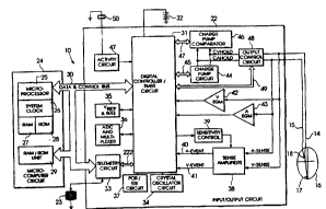
Figure 1 i~ a block diagram of a cardiac p~ r in accordance
with one : o ; -~ of the invention;
Figure 2 i~ a diagram illustrating the format of an atrial output
control register in the digital controller/timer circuit from Figure l;
Figure 3 is a diagram illustrating the format of a ventricular
output control register in the digital controller/timer circuit from
Figure ls
Figure 4 iB an illustration of the -_~hology of a pacing pul~e
proAuceA by the p~~ r of Figure l;
Figure 5 is a 80 -~ic diagram of a pump capacitor eries
charging circuit in accordance with the disclosed : o'; L of the
invsnti~n;
Figure 6 is a c~ - -t~ A~r~ of a pump capacitor parallel
charging circuit in accordance with the~ disclosed - o'~ - ~ of tho
invention;
Figure 7 is a ~-' -tiC Aj~, ~ of a parallel charge pump circuit
in accordance with the disclosed . o'~ --t of the inventionS
Figure 8 is a ~ -t~C diagram of a series charge pump circuit
in accordance with the disclosed : o'~ --t of the inventionS
Figure 9 is a ~ c A~ r of another parallel charge pump
circuit in accordance with the disclosed ~ o'; of the invention;
Figure 10 is a e - -Lic A; ~ ~ of another series charge pump
circuit in accordance with the disclosed . _'; of the invention;
Figure 11 is a ~c~ -tic diagram of the charge pump circuit in
the p~ r of Figure 1; and
Figure 12 is a e - ;~ A ~ r of the charge pump comparator in
the ~ or of Figure 1.
D15T'J~---~ DFS~l~ ON OF A D~CI~ ~C FMBODIMISNT OF T~S INV15NTION
l.cfe--ing to Figure 1, there is shown a block A~ ~_ of an
~ l~nt~hle p~ r 10 which incG.~aLes a telemetry s-~3~Lem ~n
nccordance with the p ea- ~ invention. Although the ~.e~enL invention
will be described herein in con~unction wlth a pa/ -~r 10 having a
wo 95,00203 2 1 6 5 6 8 1 PCT~US94105175
mi~-.op.ocGeeJL based architecture, it will be und.~Lood that Fa~ -k~r
l0 may bo ~ Led in any logic basod, cu~tom integrated circuit
architecture, if de~ired The F~ r shown in Figure l is
~ubstantially similar to that disclosed in co ~nAing U.s. Patent
Appl~rAtion S N 07/794,766 filed by Paul Stein and ontitled "Method
and Apparatus for T ~ ing Activity Sonsing in a Pulse G- - &Lor",
and in co ~ A~ng U.s. Patent application S N 07/870,062 filod by
Wahlstrand ot al ontitled ~Mothod and Apparatus for Rate ~-a~---ive
Cardiac Pacing" The Stoin 07/794,766 and Wahlstrand 07/870,062
arplic~tion~ aro oach hereby incG-yGLaLed horoin by ~foronca in their
entireties
Although a part~c~lar implemontation of a pA~ -k~r iB di-closod
herein, it is to be undeL~Lood that the yLa~enL invention may be
adv~nt-~ ly practiced in con~unction with many difforent types of
~ ers, such as the p-c -k ~ described in the abv a L2fe~enced
Sivula ot al patont, for e - _le, a~ well as other typos of
nt~hlo ~ic-1 dovices
In Figure l, i-~ -k~r l0 is shown to includo an activity sensor
50, which may be, for ~ _le, a F~zQelsctric el~ - ~ bonAed to the
insido of the ~-- ~kor's shiold Such a ~L- ~k?r/activity sensor
configuration is the ub~-ct of the abG _ cGfo.anc I patent to ~ L J --
t al P~e~e1ectric ensor 50 providos a sonsor output which varios
a- a function of a moa-urod par_metor that relates to tho met~hollc
r qui~ ~ of a p~t1~- L
P-~ -k~r l0 of Figure l is y~v~C -hlo by moans of an oxt-rnal
~,O~ ~ng unit (not shown in Figure l) Ono such y~v~ - suitable
for tho pu.~ 8 of tho p.~es~ invontion i8 tho MadL.onic Modol 9760
~rv~. - which i- ~ - cially availablo and is ~ntenAe~ to be u~od
with all 1~ t onic p-~ -k- ~- Tho 9760 ~,v~ a
micLv~,ec~ss~ ba-od device which provid - a ori-- of nc~g~ ignals
to ~a~ r l0 by moans of a p,vy, ~ng hoad which transmits radio-
f.~ (RF) e~o~ed signals to F~ ~k9r l0 according to tho
tele L.~ sy-tom laid out, for ~ le, in U S Patent No 5,127,404 to
W~.n~ et al ontitlod ~ _v -~d Te1 - ry Format", which is as-igned
to tho assignoo of tho p,~ invontion and which is inoo,yo.at-d
h-rein by rof_-onc_ in it- ontir-ty It is to be ~ndo.~Lood, ~ G~
that tho ~6y- ~ ~ ng mothodology di-clo-od in tho abv a ~afe~.ncGd
pat-nt i- ~d~ tifiod horoin for the yu~o~a8 of illustration only, and
that any ~;6~ ng methodology may bo employed 80 long as the dosired
information can bo con~a~_~ bet ~-- the F~ ~k~r and the oxternal
~,6~ ~ .
W O 95/00203 21 6 5 6 81 PCTrUS94/05175
It i~ believed that one of skill in the art would be able to
choose from any of a number of available pa~ r p,oy~ - ~ and
p~o~ ing techni~ues to a~ iQh the task~ n~ceseAry for practicing
the ~e~ant invention A~ noted above, ~ Je~a~, the Medtronic Model
9760 ~.OYL - i~ p~e~an~ly preferred by the inventor~
In the illu~trative o'i ~L of the p~a~enL invention,
parameter- such a- the lower rate of p-r -~er 10 may be p,o~ -hle,
for example from 40 to 90 pul~e~ per minute (PPM) in inc. t~ of 10
PPM, and the upper rate may be ~rog -hle, for ~ le, batJ6 - 100
and 175 PPM in 25 PPM inc~ . There may al~o be p.og -hle rate
re~pQn~e function~ in pAC -~r 10 In addition, pa~ ~~er 10 ha~, in
accordance with one ~ L of the ~E~f L invention, a plurality of
pr~L- -hle output pul-e energy etting~ In particular, the output
pul-e energy level i- ~ro~ -hle from 0 to 7 5-V in 0 5-V inc.~ - L~
lS P~ r 10 i~ e~ Cal ly ~hown in Figure 1 to be
electrically coupled via pacing lead 14 and 15 to a patient'~ heart 16
Lead~ 14 and 15 include one or more intracardiac electrode~, ~gpgn~in~
upon whether they are unipolar or bipolar leads A~ would be
appreciated by thoce of ordinary kill in the art, bipolar lead~
include ~eparate, electrically i-olated tip and ring electrode~, while
~nipol~r lead- include a ingle tip electrod For the ake of
illu-tration, electrode- ~ gn~t-ed as 17 and 18 are ~hown in Figure~ 1,
loc~te~ near their di-tal end- of lead~ 14 and 15, .-g~acLively, and
po~itioned within the right ventricular (RV) and right atrial (RA)
Ch `- ~, .oE~G_Lively~ of h art 16 It i~ to be ~nd6,,~Lood, h~
that lead- 14 and 15 may be of either the unipolar or bipolar type~ a~
i~ well known in the art
Fl.~L.~Pc 17 and 18 ar- couplo~ via ~uitable lead conductor~
through Lnput/output t- n~l ~ of an input/output circuit 22 In the
p,~ tly dL-clo-ed o~ ~ L, activity en~or 50 i~ b-n~-~ to the
in~ide of the ~ out-r prot-ctiv- hi-ld, in accordance with
common practice in the art A- hown in Figure 1, the output from
activLty en-or 50 iB al~o co~ple~ to input/output circuit 22
Input/output circuit 22 cQnta~ the analog circuit~ for
interface to the heart 16, actLvity ~en-or 50, an antenna 23, a~ well
a~ circuitc for the ~rpll~at~sn of ~t~ lating pul~e- to heart 16 to
control itc rate a~ a function thereof under control of the cof~J~re-
~mpl~ Led algorithm~ in a micr~ _Ler circuit 24
Mi~ LeL circuit 24 compri-e~ a mi~ op~.c~cccr 25 having an
internal ~ystem clock circuit 26, and on-board RAM 27 and ROM 28
Mi~r~o_ _~er circuit 24 further compriaes a RAM/ROM unit 29
Mi~ro~roce~acr 25 and RAM/ROM unit 29 are each coupled by a data and
control bu- 30 to a digital controller/timer circuit 31 within
input/output circuit 22 Mi~L.o _Ler circuit 24 may be a
commorcially-available, general-purpo~e mic~o~.ocaa-or or
microconLroller, or may be a cu~tom integrated circuit device r--_ ~ Led
by atandard RAM/ROM c~ _x~~-t~
W O 95/00203 2 1 6 5 6 8 1 PCT~US94/05175
It will be undec~Lood that each of the electrical c L~
~ap.~ te~ in Figure 1 i~ ~ ed by an a~p.op.iate ~ lantahle
battery power ource 32, in accordance with common practice in the art.
In the p-2~ ly di~clo~ed : ~'; - L of the invention, power ~ource 32
i~ a lithium-iodine battery. Lithium-iodine batterie~ ~uitable for the
pu.~oeaa of the ~esan~ invention are well-known and - - -ially-
ava~lah~- from a number of manufa~Lu.ec~. For the sake of clarity, the
courl~n^j of battery power to the variou~ of r~ Dr lo ha~
not been shown in the Figure~.
An nt-nn- 23 is col~ne_Led to input/output circuit 22 for
.~rer of upl~n~ n~ tol~ ry through an RF t~ -try circuit
33 in accordance with one . ~ -t of the invention, to be
hereinafter dQscribed in y-~-ter detail. In the ~ - L of Figure
1, t-le -try cireuit 33 i~ couple~ to digital eontroller/timer eireuit
31. It i8 CQnt- _ lPte~ that tel~ -try circuit 33 may al~o be coupl
directly to mi~.._ ter circuit 24 via data and control bu~ 30.
A crystal o~cillator circuit 34, typically a 32,768-Hz cry~tal-
controlled oscillator, provide~ main timing clock ~ignals to digital
controller/timer circuit 31. A VREF and Bia~ circuit 35 gena.aLes
20 stable voltage reference and bias ~u.. enLs for the analog circuits of
input/output cireuit 22. An analog-to-digital con~e~Ler (ADC) and
mult~pl---r unit 36 digitizes analog ~g~-l~ and voltages to provide
~r_al-time~ t^l :L.~ intracardiac signal~ and battery elective
replAr L ~n~r~tor (~RI) and end-of-life (EOL) functions.
A ~ ~ Oll c~c~L and elective r-plAr L ~n~CAt.^,r (POR / ERI)
cireuit 37 functions a~ a means to reset circuitry and related
funetions to a default condition upon detection of a low battery
eondition, which will occur upon initial device L_~e u~ or will
tran-iently oceur in the ~.e~- ~ of -l~ Lr~ -_ Lic intecr_-~ncG, for
~ 1-. POR / ERI circuit 37 al~o funetions to monitor the depth of
~r---rge of battery 32, as will be hereinafter described in greater
detail, and informs digital controller/timer circuit 31 when an ERI
should be issued.
In part~eula-, POR / ERI circuit 37 in accordance with the
p.~ ~- Lly disclosed ; ~ of the invention is~ue~ an ERI when the
battery ha~ cr -^h^~ a predet~ ~ n_~ level of depletion. The ~a~ -Ler~
nitored by circuit 37 in order to ~r ~ n9 the level of battery
d-pletion can be diff-rent ~ n-^J upon the part~cu~ar ~ tion
of the inv-nt~nn, and may involve, for l~, one of the prior art
~ e mea~urement ~c~ -r previously described.
The operating - '~ for controlling the timing of pa~ ^r 10
are eoupled by bus 30 to digital controller/timer circuit 31 wherein
digital timer~, regi~ters, and eounter~ are employed to e~tabli~h the
overall ee~ interval of the pa,r ~~-r, as well a~ variou~
refractory, bl~n~ng, and other timing window~ for controlling the
operation of the peripheral c ~~ ~ within input/output circuit 22.
W O 95/00203 2 1 6 5 6 8 1 PCTAJSg4/05175
Digital controller/timer circuit 31 i8 coupled to gen~l ng
circuitry including a sense amplifier circuit 38 and a sensitivity
control circuit 39. In partic~llPr, digital controller/timer circuit 31
receives an A-EVENT (atrial event) signal on line 40, and a V-EVENT
~ventricular event) signal on line 41. Sense amplifier circuit 38 is
courle~ to lead~ 14 and 15, in order to receive the V-SENSE
(ventricular sense) and A-SENSE ~atrial sense) signals from heart 16.
Sense amplifier circuit 38 asserts the A-EVENT signal on line 40 when
an atrial event (i.e.~ a paced or intrinsic atrial event) is detected,
and a~serts the V-EVENT signal on line 41 when a ventricular event
(paced or intrinsic) is detected. Sense amplifier circuit 38 includee
one or more sense amplifiers corresp~n~ing, for example, to that
disclosed in U.S. Patent No. 4,379,459 iseued to Stein on April 12,
1983, incG~GlaLed by reference herein in it~ entirety.
Sen~itivity control 39 is provided to adjust the gain of sense
amplifier circuitry 38 in accordance with ~.ogc -' sensitivity
settings, as would be appreciated by those of ordinary ~kill in the
pacing art.
A V-EGM (ventricular electrocardiogram) amplifier 42 is coupled
to a conductor in lead 14 to receive a V-SENSE signal from heart 16.
Similarly, an A-EGM (atrial electrocardiogram) amplifier 43 is coupled
to one conductor of lQad 15 to receive the A-SENSE signal from heart
16. The electrogram si~n-l B developed by V-EGM _mplifier 42 and A-EGM
amplif$er 43 are u~ed on those occ~ons when the i _lrntF~ device is
being int---og~s~ by external y-Oy~~ ~ 11, to transmit by uplink
tsl~ ~ry a ._~.G~cn~ation of the analog electrogram of the patient's
el-ctrical heart activity, uch as d scribed in U.S. Patent No.
4,556,063, issued to ~ --- et al., assigned to the a~e~gn~e of the
~.~_nL invention and incG~G~Led herein by reference.
Digital controller and timer circuit 31 is courle~ to a charge
pump circuit 44 via a plurality of control lines designate~
collectively a~ 45 in Figure 1, and to a charge pump comparator 46 via
a plurality of control lines 47. Also, circuit 31 is couple~ to an
output control circuit 48 via a plurality of lines desi~note~ as 49.
Charge pump circuit 44 .~e~ '~ to ~i~nAl~ from controller circuit 31
to ~n~t~-te the charging of output capacitors th-rein, as will be
hereinafter de~cribed in ~ tsr detail. In particul~r, and as will be
de-cribed below in greater detail, charge pump circuit 44 includes
atrial and ventricular hold capacitors (not shown in Figure 1) for
storage of charge for atrial and ventricular pacing pulses,
~ e_Lively. The atrial capacitor's charge appears on an output line
CAHOLD from charge pump circuit 44; the ventricular capacitor~s charge
appears on an output line CVHOLD from charge pump circuit 44. The
atrial charge on CAHOLD is provided to charge pump comparator 46 and to
output control circu~t 48; the ~entricular charge on CVHOLD i~ prov~ded
to charge control circuit 44 and to output control circu~t 48.
W O 95/00203 2 1 6 5 6 8 1 PcTrusg4/05l75
13
Charge pump comparator 46 ie activated in .ee~onee to eignale
from controller circuit 31 on linee 47. When activated, charge pump
comparator 46 monitore the voltage on the CAHOLD and/or CVHOLD lines
and providee eignals to controller circuit 31 indicative of the
charging level of the atrial and ventricular hold capacitore.
Output control circuit 48 ie reeponeive to signals from digital
controller/timer circuit 31 on linee 49 to cauee the voltage on the
CAHOLD and CVHOLD linee to be applied to the patient' B heart. In
part~r~ , output control circuit i8 coupled to receive the CAHOLD and
CVHOLD voltagee, and ie aleo coupled to one or more of the conductors
in each lead 14 and 15. Digital controller/timer circuit 31 providee
eignals on lines 49 to output control circuit 48 ~n~c~ting whether
unipolar or bipolar pacing hae be-n select-d for the atrial and
ventricular ch- - 8. Output control circuit 48 ~ce~ to theee
signals by co~lpl1nq the ~ op iate lead condu~Lore to eetablieh the
desired ~u ~.-L path for pacing pulsee. For example, if bipolar atrial
pacing i8 eelected, output control circuit 48 will function to couple
the two leade of bipolar atrial lead 15 to the atrial hold capacitor,
eo that atrial pacing puleee are delivered ~et a~- the two atrial
electrodes. If unipolar atrial pacing ie eelected, output control
circuit 48 functione to couple the un~pol~r pacing electrode on lead 15
and the p~ ~ 'e conducLive outer canister to the atrial hold
capacitor, eo that atrial pacing pul-es are delivered bet\~-- the
atrial tip electrode and the canieter, acting ae a common electrode.
Ae would be appreciated by thoee of ordinary ekill in the art,
input/output circuitry will include decoupllng circuitry for
t- ~ rily d~ eG, l~ng eense amplifier circuit 38, V-EGM amplifier 42
and A-~GM amplifier 43 from leade 14 and 15 when stimulating pulees are
being delivered from output control circuit 48. For the eake of
clarity, euch da~oupling circuitry ie not depicted in Figure 2.
~hile epecific : - ~ - te of eenee amplifier circuitry and EG~
Q lifier circuitry have b,een ~d tlfied herein, thie i8 done for the
.~o~ee of illuetration only. It ie believed by the inventor that the
epecific - ~ L- of euch circuite are not critical to the p.e~~ t
inv~ntin~ eo long as they provide meane for genc.aLing a et~ l~tlnq
pul-e and provide digital controller/timer circuit 31 with signale
indicative of natural and/or et~ late~ contractione of the heart. It
ie aleo believed that thoee of ordinary e~ill in the art could choee
from among the varioue well-known ~ --t~atjon~ of euch circuite in
practicing the p.~e~--L invention.
Digital controller/timer circuit 31 ie coupled to an activity
circuit 50 for receiving, proceseing, and amplifying activity eignale
receivced from activity eeneor 20. A euitable impla ~ t~tion of
activity circuit 50 ie deecribed in detail in the ab~.~ .efc.cnced
Sivula et al. ~ppllration. It ie believed that the particular
impl~ ~tAtion of activity circuit 50 i8 not critical to an
~VO 95/00203 2 1 6 5 6 8 1 PCT~US94/05175
~ndac~an~;nj of the ~.asenL invention, and that various activity
circuits are well-known to those of ordinary skill in the pacing art
As previously noted, digital controller/timer cLrcuit 31 includes
certain registers for storing digital data used in the control of
p~ r functions In the case of ~ o~- -hle functions, the
digital data c~ santing selected values for ~oy- -hle paramQters
are d~ loa~^d from an external ~c~y~ ; ng device to pa ~ r 10 via
the telf ry link As would be appreciated by those of ordinary skill
in the art, a download-d digital value can contain bits identifying the
paramet r to be p~ogc -l and bits identifying the selected value for
that parameter
one of the registers maintained ln dig$tal controller/timer
circuit 31 in accordance with the ~ ea~nLly disclosed ~ - L of the
invention is an eight-bit atrial output control regi~ter Digital
controller/timer circuit 31 uses the data in the atrial output control
register to control various aspects of atrial pacing by pac -~-r lO
In Figure 2, th re is shown a A j r ~ ~ of the atrial output control
register
Referring to Figure 2, the most significant bit (MSB) position of
the atrial output control register, i e , bit s ven, is not us d Bit
position six, des;;nAte~ AUNB, stores a binary value l~-ntifying
whether unipolar or bipolar atrial pacing is to be performed As would
be appreciated by thos- of ordinary skill in th art, unipolar atrial
pacing involves delivery of an atrial stimulating pulse ket~ a tip
electrode of a unipolar atrial lead and the conductive can of ^~- ~ker
lO, acting as a common lectrode Bipolar atrial pacing, on the other
hand, involves delivery of an atrial st~ ~at;ng pulse bet ~ - the tip
and ring electrodes of a bipolar atrial pacing lead When bit six of
the atrial output control regist-r iB a ~1~, unipolar atrial pacing is
elect-d; when bit ix is a ~O~, bipolar pacing is selected
Bit position five of the atrial output control register,
~eei~n-t~ ACPD, tores a bit which enables and disables the atrial
portion of charge pump circuit 44 Wh n the ACPD bit i8 set to ~
the atrLal portion of charge pump circuit 44 i~ disabled, resulting in
O-V atrial pacing pulses When ACPD is a ~O~, the atrial portion of
charge pump circuit 44 iB enabled, so that atrial pulses of the
~L~9C~ -' amplitude are g~naL~Led
Bit position four of the atrial output control register,
designated AREG, stores a bit for enabling and disabling charg- pump
comparator 46, as will hereinafter be described in greater detail
Wh-n the AR~G bit is a ~O~, the atrial output capacitor is charged in a
nor~al fashion without the use of charg- pump comparator 46 for
nltorLng the charge level For the purposes of the following
description, this type of charging will be referred to a~ ~unregulated~
chargLng. When the A~EG bit is a ~1~, charge pump comparator 46 Ls
enabled, such that the charging level of the atrial output capacitor is
wo gs/00203 2 1 6 5 6 8 1 PCT~US94/05175
monitored to ensure that the selected output amplitude i~ reached.
Thi~ will be referred to herein a~ "regulated" charging.
The l~- Orde four bit positions (bit po~itions three through
zero, de~ignated AAS3, AAS2, AASl and AASO in Figure 2) of the atrial
output control regi~ter atore a four-bit atrial amplitude value which
dete ~nA7 the level to which the atrial output capacitor i~ charged
and thus the ampl$tude of atrial ~timulating pulses. The atrial
~mplitude value iB interpreted in conjunction with the AREG bit; that
i~, the amplitude re~ulting from a given atrial amplitude value i~
different deFen~i ng upon whether the charge amplitude control circuit
i~ enabled or di~abled. The four-bit atrial amplitude value i~ also
interpr ted in con~unction with a bit from a ventricular output control
regi~ter, to be hereinafter described in greater detail. In
particular, the ~tate of one bit, VAS3 in the ventricular output
control regi~ter affect~ the interpretation of the four-bit atrial
amplitude value. The different atrial stimulating pul~e amplitude~
resulting from the variou~ combinations of atrial amplitude value~,
AREG value~, and VAS3 values are set forth in the following Table 1:
21 65681
W O 95/00203 PCT~US94/05175
16
TABLE 1
LOW
UN- HIGH
REGUIATE UN-
D REGUL~TED
REGUL~TE AMPLITUDE
D AMPLITUDE (AREG = 0,
AAS3 AAS2 AASl AAS0 AMPLITUDE (AREG = 0, VAS3 = 1)
(AREG = 1) AAS3 = 0,
VAS3 = 0)
0 0 0 0 05 L25 2.5
0 0 0 1 1.0 1.25 2.5
0 0 1 0 15 250 s.n
0 0 1 1 2.0 250 S.0
0 1 0 0 25 3.75 5.0
0 1 0 1 3.0 3.75 5.0
0 1 1 0 35 5.00 75
0 1 1 1 4.0 5.00 75
0 0 0 45 N/A 75
0 0 1 5.0 N/A 7.5
0 1 0 55 N/A 75
1 0 1 1 6.0 N/A 75
0 0 65 N/A 75
0 1 7.0 N/A 75
0 75 N/A 75
8.0 N/A 75
The ~N/A~ (~not avallable~) entrie~ in the ~low unregulated
amplitude~ column of Table 1 above reflect the fact that in the
p~e ltly di~closed . ~ t of the invention, the low unregulated
amplitudes are available only when AAS3 and VAS3 are both zero; if
30 either atrial or ventricular pacing pul~e~ of greater than or equal to
4.5-V are to be delivered, only the ~high unregulated amplitude~
~etting~ are available. Stated differently, ~high unregulated
amplitude~ atrial setting~ are u~ed if either AAS3 or VAS3 i~ a
Ac noted above, a ~econd regi~ter -int~ned in digital
35 controller/timer circuit 31, called the ventricular output control
regi~ter, i~ u~ed to control variou~ a~pect~ of ventricular output
pul~e j ~f a~ion, in a ----L ~nAlogou~ to the atrial output control
register. The format of the ventricular output control register i~
depicted in Figure 3.
wo gs/00203 2 1 6 5 6 8 1 PCTAUS94/05175
17
AS shown in Figure 3, the MSB position (b~t seven) of the
ventricular output control register is de~ignated SAVB. The SAVB bit,
when eet to ~1~, allows charge pump circuit 44 to be disabled when a
low power supply condition is detected, in order to conse~e the
~ n~ng available power from battery 32. This bit is set to ~1~ by
digital controller/timer circuit 31 when POR / ERI circuit 37 detects a
low power supply condition. When SAVB is ~0~, this power saving
function is disabled.
Bit position six in the ventricular output control regi~ter,
A~ign-ted VUNB, selects either unipolar or bipolar ventrlcular pacing,
~ust a~ the AUNB bit in the atrial output control register selected the
mode of atrial pacing.
Bit position five in the ventricular output control register,
doe~g~ted VCPD, is used to enable and disable the ventricular portion
of charge pump circuit 44.
The ~ n~ng four bit positions in the ventricular output
control register, designated VAS3, VAS2, VAS1, and VAS0, store a four-
bit ve~tricular amplitude value co e~nA~ng to the ~r~y~ -hly
selected ventrlcular amplitude. The four-bit ventricular amplitude
value ls interpreted in conjunction with the VREG bit and the AAS3 bit,
~ust ao the atrial amplitude value is interpreted in con~unction with
the ARBG and VAS3 bits. The dlfferent ventricular stimulating pulse
amplitudes resulting from the various combin~t~n~ of ventricular
mplitude valuQs, VREG values, and AAS3 values are et forth in the
following Table 2:
W O 95/00203 21 6 5 6 8 1 PCT~US94/05175
18
TABLE 2
LOW
UN- HIGH
REGULATE UN-
D REGUL~TED
REGULATE AMPLITUDE
D AMPLITUDE(AREG = 0,
VAS3 VAS2 VASl VAS0AMPLITUDE(VREG = 0,AAS3 = 1)
(VREG = 1) AAS3 = l
VAS3 = 0)
O O O 0 05 1.?5 25
0 0 0 1 1.0 1.25 25
0 0 1 0 15 2.50 5.0
0 0 1 1 2.0 250 5.0
0 1 0 0 2.5 3.75 5.0
0 1 0 1 3.0 3.75 5.0
O 1 1 O 35 S.00 75
0 1 1 1 4D 5.00 75
0 0 0 45 N/A 75
0 0 1 5.0 N/A 75
0 1 0 55 N/A 75
1 0 1 1 6.0 N/A 75
0 0 65 N/A 75
0 1 7.0 N/A 7.5
0 75 N/A 75
8.0 N/A 75
As with the atr$al amplitude ~alue, the ~N/A~ entries in the ~low
urL~ ted amplitude~ column of Table 2 reflect the fact that if
either VAS3 or AAS3 are set to ~1~, only ~high unregulated amplitude~
values are a~ailable.
Although ~regulated~ and ~unregulated~ atrial and ventricular
output amplitudes may be selected by digital controller/timer circuit
31 by ~ettlng the AREG and VREG bits, in the p.aoanLly preferred
~ t of the invention selection of ~regulated" or ~unregulated~
output is not a p.v9 -hle parameter that may be selected through the
35 use of an external ~rOyL~~ - The selection of ~regulated~ or
~uc~ ted~ output is done automatically by p~ Dr 10, as will be
hereinafter e~pl~ n~d in greater detail. Thu~, for each ch- - , there
are sixteen possible amplitude settings, ~Led zero through fifteen:
OFF, and 0.5-V to 7.5-V in 0.5-V inc~ 8.
AB will be appreciated by those of ordinary skill in the art, the
~ppl~c~tion of a stimulating pulse to one Ch- '- of the heart iB a
W 0 95/00203 2 1 6 5 6 8 1 PCT~US94/05175
multiple-step process. The proce~s i~ initiated by digital
controller/timer circuit 31 $n re~ponse to a predeta ~nsd set of
cond$t$ons. For e le, controller/timer c$rcuit 31 may function to
initiate delivery of a ventricular pacing pulse only when a
predete i n-d time interval elapses following a paced or natural atrial
ev nt, when no natural ventricular event i8 detected during that time
p-riod. It is believed that the details of the pacing algorithm, i.e.,
the various conditions, time intervals, algorithms, and the like that
define the pacing funct$ons of pa~ 10~ are not crit$cal to an
und.,~L~nA~ng of the ~,esGnL $nvent$on, and w$11 not be descr$bed
here$n in substantial deta$1. It is bel$eved that various pac$ng
algorithms and ~ ations of paf -~-rs are known and/or
c - cially avA1l~hle, and that the p,za ~ invention may be r_adily
~pt-d for use in differGnt systems by persons having the benefit of
the ~,asenL disclosure. For the purposes of the p e~ant d$sclosure, $t
is sufficient to state that digital controller/t$mer circuit 31
~ tB a pacing algorithm and at various times tak s st ps to
initiate delivery of atrial and/or ventricular stimulating pulses.
When controller/timer circuit 31 initiates delivery of a pacing
rul~e, it asserts on. or more s$gnals conduct d on lines 45 to initiate
the charging of the ayp,op~iate ($.e., atrial or ventricular) output
capacitor in charge pump circuit 44. A~ noted above, and in accordance
with one aspect of the p~ea ~ invention, the charging of output
capacitors by charge pump circu$t 44 may or may not also $nvolve
activation of charge pump comparator 46. If charge pump comparator 46
is r quired, it is activated by one or more signals asserted on lin-s
47 -- for xample, sign-l~ derived from the AREG and/or VREG bits in
th atrlal and ventricular output control rGgist-rs may be provided to
activate charge pump comparator 46.
The charging pha~e, which will be described below $n greater
deta$1, r-sults in a voltage stored on so-called pump capacitors in
charge pump circuit. After the pump capacitors are charged, digital
controller/timer circu$t 31 is~ues control s$gnals caus$ng charge pump
circuit to beg$n a ~ _i nj phase, where$n charge on the pump capacitors
i- transf-rred to an output, or ~hold~ capac$tor. The level of voltage
stored on the hold capacitor w$11 then rGflect the output ampl$tude
value (atrial or ventricular) stored $n the 1~DW Orde~ four bits of the
co~.Ls~A~ng output control reg$ster. The ~tored voltage level w$11
al~o refl-ct whether ~regulated~ or ~n~ lated~ charging i8
~n~fc ~'. In the case of ~regulatod~ charg$ng, during the ~ ing
pha~e the voltage on the hold capacitor is arplie~ ~via either the
CAHOLD or vaHoLD line) to charge pump comparator 46, which asserts an
output signal only when the stored voltage reaches the desired level,
measured in multiples of a 1.2-V reference voltage that is also applied
to charge control circuit. The output from charge control circuit is
provided to control circuit 31, which .~Eyo~A~ to the charge control
s$gnal to stop the ~ _~ng phase. In the case of ~unregulated~
wo 95,00203 2 1 6 5 6 8 1 PCT~US94/05175
charging, charge pump comparator 46 iB not activated, and the voltage
establirhed on the output capacitor i~ ~ OpG~ Lional to the output
voltage from battery 32. The manner in which thi~ is ~ hD~ will
be described in greater detail below.
After the de~ired voltage ha~ been ~tored on the pump capacitor~
and then ~ ~ onto the de~ired output capacitor, digital
controller/timer circuit 31 a~sert~ the app~op.iate ~ignal~ on line~ 49
to cause the output capacitor to be momentarily coupled to the
~pro~iate conductor(~) of one of the lead~ 14 or 15. In Figure 4,
there i8 shown a waveform of a typical pacing pul~e delivered to the
patient'r heart. Note from Figure 4 that it iB actually a negative-
going voltage pul~e that i8 applied. The peak (i.e., mo~t negative)
pacing pul~e voltage i~ de~ignated in Figure 4 a~ Vpk. The width of
the pulse, which cG.~ A~ to the time interval during which the hold
capacitor ir coupled to the pacing lead~ designated a~ tp~. The
pacing pulse ~amplitude~, which co..æ~po~Q to the ~ettings of Tables 1
and 2 above, ir ds~i~n~te~ a~ Vp in Figure 4. Note that the pul~e
amplitude Vp is mea~ured at a point 250-~Sec after the beginning of the
pacing pul-e.
Turning now to Figure 5, there i~ rhown a circuit illu~trating
one configuration of charge pump circuit during the charging phare. A~
will hereinafter be further eYplai n~ with reference to later Figures,
charge pump circuit 44 ir a versatile circuit which i~ re~ponsive to
variou~ ~ ~nationr of control signals to achieve different
configurations of _ ~-~ ts therein. Thus, the circuit of Figure 5 is
an eguivalent circuit rhowing how charge pump circuit 44 operates in
one in-tance. In par~ r, the configuration of Figure 5 depictr the
tate of charge pump circuit 44 during one type of charge pha~e, called
a ~rerial charge~.
The circuit of Figure 5 includes two pump capacitor~, de~ignated
CPl and CP2. Capacitors CPl and CP2 are, in the configuration of
Figure 5, coupl~~ in series ~e~eE- the t. ~nat~ of battery 32, ro
that one-half of the battery voltage ir stored on each capacitor CPl
and CP2.
In Figure 6, there i~ ~hown a circuit illurtrating another
pogrible configuration of charge pump circuit 44 during the charging
phase. The configuration of Figure 6 ir called a ~parallel charge~, in
which pump capacitor~ CPl and CP2 are couple~ in parallel be~J~-- the
te ~n-lP of battery 32. With the configuration of Figure 6, the
entire battery voltage ir ~tored on each capacitor CPl and CP2.
Turning now to Figure 7, there is shown a circuit for one
porrible configuration of charge pump circuit 44 during the pumping
phase, during which pha~e charge previou~ly stored on pump capacitors
CPl and CP2 during the charge pha~e are ~ppl~ to a hold capacitor,
~sr~n-te~ ar CHO~D in Figure 7. It is to be und6.~Lood that hold
capacitor CHOLD in Figure 7 may be either the atrial hold capacitor
Q HO~D or the ventricular hold capacitor CVHOLD, as will hereinafter
W O 95/00203 2 1 6 5 6 8 1 PCT~USg4/05175
~o- - more apparent The pumping circuit configuration of Figure 7
will be hereinafter referred to as a ~parallel VDD~ arran3 t, since
the ~ _ing capacitorB are coupled in parallsl to the po~itive (VDD)
t e i na 1 of battery 32
In Figure 8, there is shown a circuit for another possible
configuration of charge pump circuit 44 during the ~ _ ing phaBe.
Again, capacitor CHOLD in Figure 8 may be either the atrial hold
capacitor Q HOLD or the ventricular hold capacitor CVHOLD The pumping
circuit configuration of Figure 8 will be hereinafter referred to as a
~-eries Vw~ arra~
In Figurs 9, there is shown a circuit for still another po~sible
configuration of charge pump circuit 44 during the ~ ~ng pha~8~
wherein capacitor CHOLD may bs either the atrial or ventricular hold
capacitor The ~ _~ n7 arr~-~ L of Figure 9 will be hereinafter
rsferrsd to as a ~parallel Vss~ arra-, --t, since the pump capacitors
CPl and CP2 ars coupled in parallel to the negative (Vss) te inal of
battery 32
Finally, in Figure 10, there is shown a circuit for another
po-~ible configuration of charge pump circuit 44 during the ~ ~ n~
pha~s The ~ n,ing a~ of Figure 10 will be hereinaftsr
~fe r~' to a~ a ~-eries Vss~ a~ ~n, --~
A- will be appreciated by tho-e of ordinary kill in the circuit
art, wlth ths two poee~hle charging configurations, parallel and
ssrial, and the four possible ~ _~ng configurations, parallel and
srial V~ and parallel and erial Vss, there are eight possibls
chargs/pump ~v~.~ B which can be performed, each rssulting in a
diffsrent charge being ~ onto the hold capacitor In the
following Table 3, thers is st forth the sight holding capacitor
voltags- which can be achievsd with ths eight different possible
charge/pump ~e, ~ ~e~
TABLE 3
HOLDING
CHARGING MODEPUMPING MODE CAPACITOR
VOLTAGE
SERIES p~R~TT~T Vr~ 1/2 x Vnn
35SERIES SERIES Vnn Vnn
SERIES pAR~TT~T Vee 3/2 x Vnn
SERIES SERIES Vcc 2 x Vnn
pp,RAT.TYT. pARAT~TyT- V~n 1 X VDD
pAR~T.TYT. SERIES V~ 2 x Vn~
40p~ T.T.li!T.pA~I~T-T-~T- Vee 2 x V~
p~T.T.~T. SERIES Vee 3 x Vnn
Turning now to Figure 11, there is shown a ~e~ -~ic diagram of
charge pump circuit 44 in accordance with the p~e~e -ly disclosed
45 ~ ment of the inventio~ The circuit of Figure 11 includes the two
WO 95/00203 2 1 6 5 6 8 1 PCT/US94/05175
~ _ in~ capacitors CP1 and CP2 and the two hold capacitors CAHOLD and
CVHOLD. AR will be appreciated by those of ordinary _kill in the art,
the circuit of Figure 11 i8 capable of charging the two pumping
capacitors CP1 and CP2 in either the parallel or serial modes described
above, and is additionally capable of ~ ; ng both the CAHOLD and
CVHOLD capacitor_ in any of the four charging mode~ (parallel and
serial VDD and Vss). The different charge/pump sequenceR are controlled
by mean_ of the various Rwitches in the circuit of Figure 11, which
switches are actuated by control signal_ provided to charge pump
circuit 44 on line_ 45 (see Figure 1) from digital controller/timer
circuit 31. It i_ to be ~nda-~-ood that in the Figures, referencec to
VDD ._pC~ ~ conne_LionR to the positive t inal of battery 32 while
ref~ren~ee to Vss ~.36en~ connecLions to the negative te: inal of
battery 32.
Charge pump circuit 44 of Figure 11 includec a plurality of
ewitches, de~iqn~toA ~ SW1 through SW 11, which in the p a~ently
preferred . `~ L of the invention are implemented a~ cimple FET
devices. Although it is not shown in Figure 11, switches SW1 through
SW11 are controlled (i.e., opened and closed) in recponce to control
signals provided from digital controller/timer circuit 31. In
particulnr, digital controller/timer circuit 31 control~ charge pump
circuit 44 with a four pha~e clock e~e~e to (1) charge pump
capacitor_ CP1 and CP2; (2) pump atrial hold capacitor Q HOLD; (3)
charge pump capacitors CP1 and CP2; and (4) pump ventricular hold
capacitor CVHOLD.
In charging phases one and three, switches SWl through SWll are
configured by controller circuit 31 to charge pump capacitors CPl and
CP2 in either the eri-_ or parallel charging mode, ~9p9nA~ng upon the
voltages to be developed on the ~. ~e_tive atrial and ventricular hold
capacitor_ Q HOLD and CVHOLD. For s le, if serie~ charging iR
required during clock phases one or three, controller circuit 31
actuates (closes) switches SWl, SW5, and SWll. Thi_ establiRheR a path
be5i nn~ ~q at the Vw conns_Lion de_~qn~ted as 100 in Figure 11, through
switch SWl, across capacitor CPl, through a 40-n resistor des~qn~te~ a~
102 in Figure 11, through switch SW5, across capacitor CP2, and then
through switch SWll to the V~ connac~ion designated a~ 104. As will
be appreciated by those of ordinary skill in the art, the configuration
~ust described co e~onds to the serial charging a.._ , - -
previously described with reference to Figure 5.
If parallel charging is required during phases one or three of
the charge pump sa~ a, controller circuit 31 assertc control signalc
to actuate (close) switches SWl, SW6, SW7, and SWll. With this switch
configuration, a first charging path is established beginning at VDD
c~ e ~ion 100, through pump capacitor CPl and recistor 102, and then
through w~tch SW6 to a Vss co~ec~ion designated ~c 106 in Figure 11.
A second path is established beginning at a VDD conna~ion designated
a~ 108 and exte~ ng through switch SW7, pump capacitor CP2, and
W O 95/00203 2 1 6 5 6 8 1 PCT~USg4/05175
through switch SW11 to Vss connrcLion 104. Thi~ configuration of
switches result~ in the parallel charging arrA- -t previou~ly
de~cribed with refe~ence to Figure 5, in which pump capacitor~ CP1 and
CP2 are coupled in parallel be!t-e - the positive and negative t~ inAl8
5of battery 32.
In charging phase~ two and four, switche~ SWl through SW11 are
operated to pump the atrial ~pha~e two) and ventricular (pha~e four)
hold capacitor~ CAHOLD and CVHOLD, ~s~cLively. Again, ~witches SWl
through SW11 are selectively actuated by control signals is~ued by
10controller circuit 31.
The four different ~ ~ng modes (parallel and eeries V~ and Vss)
are ~f- r~ h~d through the actuation of different combinations of
~witches SW1 through SWll, as ~et forth in the following Table 4:
TABL~ 4
15PUMPING MODE CAPACITOR TOS~l,~n~S ACTUATED
CHARGE (CLOSED)
pp~TT~T V,- CAHOLDSWl, SW3, SW7, SW9
SERIES V, CAHOLD SW1, SW5, SW9
p~T.T-~T- Vee CAHOLDSW2, SW3, SW8, SW9
SERIES Vse CAHOLD SW2, SW5, SW9
20pA~AT.T~T- V, VAHOLDSWl, SW4, SW7, SW10
SERIES VDr VAHOLD SW1, SW5, SW10
pA~ATT~T Ve~ VAHOLDSW2, SW4, SW8, SW10
SERI~S Vee VAHOLD SW2, SW5, SW10
As will be appreciat-d by tho~e of ordinary skill in the circuit
art, each of the ~witche~ SW1 through SW11 in charge pump circuit 44 of
Figure 11 has an ~ ncg a~ociated therewith, a~ set forth in the
following Table 5:
TABLE 5
30 SWITCH IMPEDANCE
SN1 550-~
SW2 550-Q
SW3 4700-Q
SW4 4700-n
SW5 720-Q
SW6 900-Q
SW7 565-Q
SW8 4365-~
SW9 925-Q
SW10 925-Q
SW11 925-n
W 0 95/00203 21 6 5 6 8 1 PCTnUs94/0sl7s
24
The ~witch i ~'sn~e~ ted in Table 5 are preferably ~elected
~uch that when pa~ sr 10 i~ operating at 400 beat~ per minute (BPM)
th-re is at ~t a 25% pacing pulse amplitude 10B~ and when par -~r
10 iu operating at 180-8PM there is at mo~t a 10~ amplitude lo~u, for a
supply voltage of 2-V. The ~ ne-u were al~o cho~en uch that there
i~ a ~n~ po~ible ~ur~ent drain resulting from operation of charge
pump circuit 44. It ~hould be noted that the time con~tant~ for
charging and ~ ~ng are relatively large with .a~e~L to the time
allowed for charge tran~fer. In particular, each pha~e of the four
pha~e ~e~u~ræ establi~hed by controller circuit 31 last~ for 244-~Sec,
~o that only 244-~Sec i~ available for each charge tran~fer. Thi~
meanu that charge transfer i~ not completed in each phaee of the four
pha~e charge/pump ~e~u ~æ. The - ~ total switch ; -snre which
re~ultc from each of the ~eriss and parallel charging and pumping
configurations, along with the ~n~ ~erce~tage of charge tran~fer is
et forth in the following Table 6:
TA8LE 6
~AYTY~ ~AYTYU`~ hlNl~U~S
EQUIVALENTEQUIVALENT CHARGE
RESISTAN OECAPACITAN-OETRANSFER
SERIES 2235-~ 0.055-~F 86%
CHARGE
pAPAT.T.T~T.1490-~ 0.220-~F 52%
C~ARGE
SERIES 2235-n 0.055-~F 86%
PUMP
pAP~T.T.T~T. 2645-n 0.220-~F 34%
PUMP
Due to the ~- lete charge tran~fer during the charging pha~e,
there i~ come interaction ~c~ ~~ atrial and ventricular holding
capacitor~. Thi~ re~ult~ in a ul~ghtly decreased pacing amplitude in
ca-e~ where there i~ a ~hort A-V interval or a ~hort V-A interval in
the pacing cycle. It i~ believed that for wor~t-ca~e A-V interaction,
e.~ the --~ ventricular amplitude 10~B i~ lee~ than 5%.
A~ previou~ly ~c~ ed with refe~enca to Figure~ 2 and 3, atrial
and ventricular output operation i8 controlled according to bit~ in an
atrial output control regi~ter and a ventricular output control
regi~ter. In part~c~lar, the bits of the~e regi~ters defined the
charging and ~ _ing configurations to be u~ed. The ~eries charging
mode (Figure 5) i~ uced if VAS3 and AAS3 are both low; thi~ co~ nds
to ~ ulated~ output amplitude choice~ of 1/2 x VDD, VDD, 3/2 x VDD,
or 2 x Vw. If VAS3 or AAS3 i~ high, the parallel charging mode i~
u~ed; thi~ co ~ '~ to either atrial or ventricular pacing amplitude
cet to 3 8 VDD. For thi~ ca~e the ~unregulated~ output amplitude
choice~ are 1 8 Vw~ 2 X VDD, or 3 8 VW. The po~ibility of charging
the pump capacitor~ differently for atrial and ventricular pumping
cycles i~ ~el~hsrately el~ ;n9ted in the p a~e.Lly preferred . '-'i --t
W O 95/00203 2 1 6 5 6 8 1 PCT/USg4105175
of the invention, to ~ c~nt exce~sive cu..~n~ drain. If different
mode~ for atrial and ventricular charging were allowed, the wasted
..ent would be on the order of 300-~A.
The ~ ~ ng mode~ for ventricular and atrial hold capacitor~
S CVHOLD and CAHOLD are det~e in~d by AS3, AS2, and AS1 according to the
following Table 7:
TABL~ 7
VAS3 AS3 AS2 AS1CHARGINGPUMPING AMPLITUD
OR MODE MODE E
AAS3
0 0 0 0 SERIESPARAILEL VDD 1/2 ~ VDD
0 0 0 1 SERIESSERIES VDD 1 S VDD
0 0 1 0 SERE~SPARALLEL VSS 3/2 ~ VDD
0 0 1 1 SERIESSERIES VSS 2 ~ VDD
1 0 0 0PARAI--ELPARALLEL VDD1 2C VDD
0 0 1P~RALLELSERIES VDD 2 ~ VDD
0 1 0PARALLELPARAI~eL VSS2 2~ VDD
0 1 1 PARAI~LSERIES VSS 3 ~ VDD
X XPARAII~LSERIES VSS 3 ~C VDD
Turning now to Figure 12, there i- shown a ch -tic diagram of
eharge pump eomparator 46 previously ~reu~ed with reference to Figure
1. Charge pump comparator 46 i8 used to set ~regulated~ pacing
amplitude~, by dete~ ining when the atrial and ventricular hold
eapacitor- CAHOLD and CVHOLD have been ~ r~ to the p.~
amplitude, and then shutting off the charge pumps. Charge pump
eomparator 46 u~e- a witch eapaeitor digital-to-analog con~a.Ler
cireuit refe-~need to a reference voltage VREF provided from VREF and
bias eireuit 35. Charge pump eomparator 46 includes a differential
amplifier 120 to eompare the ~Gy -~ amplitude to the voltage on the
hold eapacitor at the end of each atrial and ventricular charge ~ g
pha~e. Charge pump eomparator 46 effectively has 16 thre~holds spaced
in 0.571-V in~ , resulting in 0.5-V inc.. ~ t~ for regulated
paeing amplitudes when the amplitude i~ mea-ured from tip-to-ring on a
bipolar lead or tip-to-ca~e on a unipolar lead, 250-~Sec from the
falling edge of the negative-going pul-e, as previously de~cribed with
refL.~ to Figure 4. P.og. i ng the amplitude eleet bit~ in the
atrial and ventrieular output eontrol regi~ter~ sets the comparator
threshold.
~n addition to differential amplifier 120, eharge pump comparator
eomprises an array of bina-~ w~ig~ted eapaeitors 122, 124, 126, 128,
and 130, and an input eapaeitor 132. Capacitor 122 has a eapaeitanee
that i~ twiee that of eapaeitor 124. Capaeitor 124, in turn, has a
eapaeitanee twiee that of eapaeitor 126, whieh ha~ a eapaeitanee twiee
W O 95/00203 2 1 6 5 6 8 1 PCTAJS94/05175
that of capacitor 128. Capacitor~ 128 and 130 have the ~ame
capacitance. A ~witch 136 operate~ to selectively connect the CVHOLD
capacitor from charge pump circuit 44 to charge pump comparator 46,
while a switch 138 operate~ to a ~electively connacL the CAHOLD
capacitor to charge pump comparator. When either CAHOLD or CVHOLD i~
co~rled to charge pump comparator 46, the voltage thereon is applied to
the top plate~ of all of the bina,~ ~ighted capacitor~ 122, 124, 126,
128, and 130.
A ~witch 134 i~ coupled bBt.~ ~-1 the inverting input and output of
differential amplifier 120. During the fir~t of the four charge/pump
~9,~ e phase~ (i.e., the pump capacitor charging phase), ~witch 134
i~ closed, to zero the comparator by eli in~ting any charge left over
from a previous comparison. Closing ~witch 134 also reduce~ the
effects of offset in the fir~t stage of the comparator.
The output from differential amplifier iQ coupled to one input of
a NAND gate 140, the other input of which being coupled to receive a
signal NQ2 from controller circuit 31. The ~ignal NQ2 iQ at a high
logic level whsnc.ac ~witch 134 is not closed. The output of NAND gate
140, designated COMPARE OUT in Figure 12, i~ the output ~ignal produced
by charge pump comparator 46. The COMPARE OUT signal i~ provided to
controller/timer circuit 31 to provide an indication of the results of
comparison~ pe~fr ~' by comparator 46. The non-inverting input of
differential amplifier 120 receiv 8 a voltage that i~ one diode drop
below Vw. Thus, when ~witch 134 i8 closed to zero the array, the
voltage on the top plates of all of the bina-~ weighted capacitors 122,
124, 126, 128, and 130 i8 driven to a voltage of about 0.5-V below Vw.
Al~o while ~wltch 134 i~ clo~ed, the bottom plate~ of all of the
bina.~ weight~d capacitors 122, 124, 126, 128, and 130 are coupled, via
ewitch-s 142, 144, 146, 148, and 150, ~ea~acLively, to the referenc-
voltage VREF. Addit~nn~ ly~ while switch 134 i~ closed, the bottom
plat- of input ~ ng capacitor 132 is couple~d, via a switch 152, to
VW .
Charge pump comparator 46 operates under control of a plurality
of signals provided on line~ 47 from controller circuit 31. During the
atrial hold capacitor ~ ~ n~ pha~e, switch 134 i8 opened, and the
bottom plate of input capacitor 1132 i~ coupled, by closing switch 138,
to the CAROLD capacitor. Thi~ cau~e~ a negative ~hift in voltage on
the top plate of capacitor 134 which is y.opo.Lional to the voltage on
CAHOLD. A short time later, some of the bottom plate~ of the binary-
w~htod capacitors are coupled to VDD, via some combination of
witches 154, 156, 158, 160, and 162, causing a positive shift in the
voltage on the top plate~ thereof which i~ y-oyo.~ional to the
amplitude code in the atrial output control regi~ter. In particular,
th- capacitors who~e bottom plates are couple~ to VDD i~ det- ~ n~d by
th amplitude code, as would be appreciated by those of ordinary skill
in the circuit art.
wo 95,00203 2 1 6 5 6 8 1 PCT~US94105175
Charge pump comparator then det~ ine8 whether the net change in
voltage on the top plate i~ po~itive or negative with .eg~e~L to the
value on CAHOLD at the end of the ~ ing phase. If the voltage i~
negative, then the voltage acros~ CAHOLD i~ larger than the ~G~
amplitude and the COMPARE OUT ~ignal will be at a low logic level.
This indicate~ to controller circuit 31 that charge pumping for the
atrial side should be disabled. The COMPARE OUT ~ignal is latched by
digital controller/timer circuit 31 at the end of each pump cycle,
before switch 134 i~ clo~ed again to zero the array in preparation for
another comparison.
A small amount of hysteresi~ can be provided by coupling a small
metal-to-poly capacitor bet~ef- the input and output of comparator 46.
This provides apprQr~ -Lely l.l-mV of hystere~is at the input, and
force~ the comparator output to sit at one of the lower power ~upply
rails, lowering ~u-,en- drain at the output of comparator 46.
Comparison for the CVHOLD capacitor is performed exactly as
de~cribed for CAHOLD, except that it occurs during the fourth of the
four charge/pump _3~en-e phases.
Charge pump comparator 46 i~ also used when a new amplitude is
first p,oy.~ -~ into the atrial or ventricular output control
register~. P.~. ming a new atrial or ventricular amplitude causes
the charge pumps in charge pump circuit 44 to be hut off and starts a
~~ch-rge of the ~prop~iate hold capacitor. Charge pump comparator 46
monitors the hold capacitor voltage to ~st- ~ n9 when it drops below
the ~r~. - value. When thi- occurs, the ~ rge i~ di~continu-d
and the charge pumps are restarted.
Tn accordance with the p,_~ nLly disclosed ~ t of the
inv~nt~on, ~ ted~ amplitudes are obtained by not u~ing charge
pump comparator 46 to shut off the charge pump~. The charge pumps are
~ ~ to run CQntinUoU~ly~ resulting in the - ~ possible
amplitude for each of the p _~n7 mode~. Tt is to be unde.dLood that
charge pump comparator 46 is still used when a new amplitude i~
~.o~ -'.
~r-,_1~ate~ pacing amplitudes will begin to degrade when the
~upply voltage from battery 32 get~ small -- _ to p.~.Gnt charge pump
circuit 44 from being able to charge the hold capacitors to pr~y~ -~
threshold of comparator 46. When this ha~Fen~ the ~regulated" pacing
amplitudes will begin tracking the ~n~ ted~ amplitudes. For
'reg~ te~ amplitude~ less than or equal to 6-V, the ~regulated~
voltages will not begin to droop until the battery voltage drops below
appro-~ -tely 2.3-V.
Having described charge pump circuit 44 and charge pump
comparator 46 in some detail, operation of pac -~r lO in accordance
with the ~,_se.Lly disclosed ~ L of the invention will now be
generally described. As noted ~bo~e, pr~ r lO in accordance with
the ~ tly disclosed embodiment of the invention offers ten
pr~y~ ~~le pacing pulse _mplitude setting~: 0.5-, l.O-, l.5-, 2.0-,
wo gs/00203 2 1 6 5 6 8 1 PCTAJS94/05175
28
2 5-, 3 0-, 3 5-, 4 0-, 5 0-, and 7 5-V In accordance with one
feature of the p~- Lly di~clo~ed t '-'; - t, ~ome of the p.G9C ~hIe
amplitude~ are ~ ed a~ "regulated~ setting~ for which charge
pump comparator 46 i~ used to ensure that output pul~e~ are g~ne.&ted
at the desired _mplitude In the ~ a~an-ly preferred ~ L of the
invention, the 0 5- to 2 0-V, 3 0- and 4 0-V ~etting~ are impl~ --ted
a~ ~regulated~ ~etting~ Since these etting~ are ~regulated", pacing
pul-e~ at the~e amplitude ~etting~ are delivered at a stable amplitude
until the voltage from battery 32 declines from its beginning-of-life
(BOL) level of 2 75- to 2 8-V, to around 2 0- to 2 3-V
The ~ -ining ~etting~ in the p,ascntly preferred -'; L of
the invention (2 5-, 3 5-, 5 0- and 7 5-V) are implemented as
~n~ lated" amplitude~, for which charge pump comparator 46 i~ not
activated The~e "un~e~ulated" setting~ are more current-efficient,
15 since the additional ~u.. e L drain of charge pump comparator 46 i~
oli in-t-d, but have the characteristic that the delivered amplitude
with the~e ~etting~ declines in y-~G-Lion with the decline in battery
voltage
In pac ~~-r 10, POR / FRI circuit 37 i~ue~ an elective
repl~- ~ L ~n~ tor (ERI) when it detect~ that battery 32 i~ at lea~t
one-third depleted and that battery voltage ha~ drop~ed to a con~istent
level of apprnY~ -Lely 2 6-V Although the~e are the p.a~enLly
~ ~fe~E~ ERI criteria, it i~ c~nt~ _lrt-d that variou~ other in~icja
of FRI may be monitored in order to establi~h an ap~.~.iate ERI
In accordance with an important feature of the p.e~GnL invention,
when the ERI i~ ued by POR / FRI circuit 37, p~ -r 10 witches
to ~ ti~n~ of all etting~ other than 5 0- and 7 5-V With this
a~. r_ - t, the expected longe~ity of p~~ r 10 (or, more
~pecifically, of battery 32 in ~ or 10) i~ adv-nt~j ~u~ly
in~. ~~e~ Thi~ a ran3 - t differ~ from the prior art, in which
.ant c_ _ inq ~reg~lDti~n~ circuitry is ut~ ed in the early and
~le stage~ of battery ~oplet~on, and di~abled near the battery'~ EOL
to ~ re . ~ining u~eful battery life
Since the hardware of p-~ -~or 10 ~u~o.L~ ~regulation~ of all
u ~.~g~ -hle amplitude etting~, it i~ oont _lated by the
inventor- that other comb~n-t~n- of ~regulated~ and ~un~a,ulated~
operation, pre- and po-t-FRI, can be advant~ ly ~ _l - ted
For ~ _le, it i~ cont~ lPt-d that all amplitude etting~ le~
th~n 5 0-V could be ~ l- - od a~ ~-e; ~tsd~ ThL~ offer~ the
advantage of accuracy in delivered amplitude~ les~ than 5 0-V, but may
reduce expected longevity
Another variation to the di~closed ~ of the invention i8
to cauce the ~witch from ~unregulated~ to ~regulated~ for certain
etting~ at a time either before or after ERI It i~ cont~,lat-~ that
the criteria for deciding to make thi~ witch i~ not inherently related
to ERI criteria, and that ~ome other combination of condition~ may be
used to trigger the ~witch to "regulation~ of output amplitude~
W O 95/00203 29 2 1 6 5 6 81 PCTnJS94/05175
From the foregoing detailed de w ription of a preferred
of the invention, it ~hould be apparent that a p~ er having
p~Vyl -hly ~electable output amplitude~ has been di~clo~ed. The
p~ r include~ ~regulation" circuitry for controlling the amplitude
of delivered pul~e~. For ~ome ~etting~, the ~regulation~ circuitry i~
not ut~ze~ until near the end of the battery'~ life, ~o that
c~ _~ion of ~ nt by the circuitry i~ i n i i z~ .
Although a ~pecific . ~ of the invention ha~ be de~cribed
herein in ~ome detail, thi~ ha~ been done for the purpo~e~ of
illu~trating the ~e~n~ invention only, and i~ not intended to be
limiting with ~e~L to the ~cope of the invention. It i~ beliered
that variou~ ~ubstitution~, alteration~, and dification~, including
but not limited to tho~e ~pecifically ~i~cun~e~ above, may be made to
the di~clo~ed ~ t without departing from the ~pirit and ~cope of
the ~E- t invention a~ defined in the ~.p~d~ claim~, which follow.