Note: Descriptions are shown in the official language in which they were submitted.
2165712
METHOD FOR REDUCING BIREFRlNGENCE IN OPTICAL GRATINGS
FIELD OF THE INVENTION
This invention relates generally to a method for reducing birefringence in an
integrated optical grating, and more particularly to a method employing a beam of
5 radiation for reducing birefringence in an optical grating.
BACKGROUND OF THE INVENTION
Optical devices such as waveguides, gratings, and switches, for example, are
typically fabricated in layers of silica deposited on silicon. One problem that occurs
when employing these materials is that strain birefringence arises because of the large
10 thermal expansion coefficient of silicon relative to silica. As a result of this
difference, large compressive strains are produced in the silica layers after the
requisite annealing step is performed during the fabrication process. The resulting
birefringence caused by the strains produce different propagation constants for the
TE and TM waveguide modes. Because the modes have dirr~l~nt propagation
15 constants, an optical signal prop2g~ting in a device with maximum tr:~n~mi.c.~ion at a
given wavelength is split into two components corresponding to the TE and TM
modes. The components are thus spaced apart in wavelength and the difference,
which is referred to as the polarization shift, is typically about 0.3 nm. A polarization
shift of this magnitude is too large for many applications in which optical devices are
2 0 employed. For example, frequency routing devices having channel spacings of less
than 2 nm are required for long-haul or local area networks. For such purposes the
routing device typically should have a polarization shift of less that about 0.1 nm.
It is known that birefringence in silica waveguides is affected by irradiation.
For example, copending Application [Greene 5-1-3]entitled Radiolytic Modification
2 5 of Birefringence in Silica Planar Waveguide Structures, filed in the U.S. Patent and
Trademark Office on the same date as the present application, discloses a method for
reducing or elimin:~ting birefringence in silica waveguides by irr~ ting the
216~712
waveguides at a wavelength that induces compaction in the waveguide cladding. Inaddition, Hibino et al, Electron. Lett., 1993, 29, pp. 621-623, indicates that
birefringence can be reduced by irr~ ting the material at a wavelength which is
absorbed by photosensitive defects. Hibino irradiated one of the two waveguides in
5 a Mach-Zehnder interferometer to induce birefringence while shielding the other
waveguide with a mask. Because only two, relatively widely spaced waveguides
were involved, this arrangement was sufficient to direct the radiation to a selected
one of the two waveguides.
The irradiation method disclosed by Hibino is not satisfactory when applied
10 to an integrated optical grating rather than a Mach-Zehnder int~lrelo"leter. Optical
gratings include more than two waveguides (and typically include 1040 waveguides)
which are separated by as little as 50 microns. In this case the waveguides cannot be
selectively irradiated by masking individual ones of the waveguides. Moreover, since
Hibino simply observes that birefringence is affected by radiation, Hibino provides no
15 criteria that can be applied to determine the relative amounts of radiation that should
be imparted to the different waveguides in an optical grating to reduce birefringence.
SUMMARY OF THE INVENTION
The present invention provides a method for reducing the inherent
polarization shift caused by birefringence between the TE and TM modes of an
2 0 optical signal prop~g~ting in an optical grating which has a plurality of waveguides.
The method includes the step of irradiating the waveguides of the optical grating for
dirrt;r~l~t periods of time to induce a compensating polarization shift that substantially
reduces the inherent polarization shift. If desired, a compensating polarization shift
may be induced which not only reduces but also substantially elimin:-t~s the inherent
2 5 polarization shift.
In one embodiment of the invention, the irradiation step is performed by
scanning an irradiating beam across the waveguides at a sc~nning velocity that differs
from waveguide to waveguide. By using a sc~nning beam, the value of the
216~12
compensating polarization shift imparted to the individual waveguides may be
precisely controlled even when the waveguides are closely spaced to one another.
BREF DESCRIPTION OF THE DRAWINGS
FIG. 1 illustrates an example of a conventional optical frequency routing
5 device.
F~G. 2 shows an optical grating that is illuminated with an irradiation
arrangement in accordance with the method of the present invention.
FIG. 3 shows an illustrative example of a transmission spectrum produced by
an optical grating that is part of a conventional frequency routing device.
FIG. 4(a) shows a graph of the sc~nning time for the irradiation arrangement
shown in FIG. 2 which is used to compensate for birefringence and FIG. 4(b) shows
a graph of the scanning time which is used to compensate for both birefringence and
aberrations due to phase errors.
FIG. S shows an alternative irradiation arrangement that employs a slit
15 through which the radiation passes before reaching the optical grating.
FIG. 6 shows a detailed view of the slit and optical grating shown in FIG. 5 in
which multiple reflections are absorbed by the grating to increase efficiency.
FIG. 7 shows a mask that may be placed over the optical grating to produce a
periodic variation that approximates the required sinusoidal induced phase shift.
DETAILED DESCRIPI ION
An optical grating is defined as a plurality of waveguides having unequal
lengths that provide a predetermined path length difference when traversed by optical
signals propagating therein. In some cases adjacent waveguides in the grating all
2 5 differ in length from one another by a constant predetermined amount. The path
length difference imparts a shift in the phase of the optical signals relative to one
another. While one of ordinary skill in the art will recognize that the present
invention as set forth below is equally applicable to any integrated optical grating, the
216~71~
- 4
present invention will be described in terms of an optical grating that is a part of a
conventional frequency routing device such as disclosed in U.S. Patent Nos.
S,002,350 and S,136,671.
FIG. 1 shows the pertinent details of a conventional frequency routing device.
5 The frequency routing device contains a plurality of input ports 2j, i= l, 2, ..., N
connected to the input circle 95 of a free space region 98. A plurality of output
waveguides 30 extends from the output circle 97 of the free space region 98 and is
connected to an optical grating 32. The optical grating 32 comprises a plurality of
unequal length waveguides 391~ 392.... 39M which provides a predetermined
1 0 amount of path length difference to a corresponding plurality of input waveguides 34
connected to the input circle 33 of another free space region 46. The waveguides391 ~ 392, . ..39M that form the optical grating 32 are denoted sequentially from the
shortest waveguide 391 to the longest waveguide 39M. The output circle 35 of thefree space region 46 is connected to a plurality of output ports 4k, k= 1, 2, ..., N. The
1 5 various input and output ports are formed from waveguides. These frequency
routing devices operate as multipiexers and demultiplexers of optical frequencies.
Additional details concerning these routing devices are found in the above-referenced
patents.
Compressive strains in the silica material of which the integrated optical
2 0 grating is composed give rise to birefringence. Birefringence in turn gives rise to
different propagation constants for the TE and TM modes of an optical wave
propagating in the waveguides of the optical grating. The different propagation
constants for the TE and TM modes yield a difference in the phase shift experienced
by the two modes as they propagate. The relative phase shift between the two
2 5 modes splits the peaks appearing in the transmission spectrum of the grating into two
distinct peaks. The wavelength separation between these peaks will be referred to as
the inherent polarization shift observed in the tr~n~mi~.sion spectrum.
To reduce or even elimin~te the inherent polarization shift, the phase shift
experienced by the TE and TM modes must be adjusted to compensate for the effects
- 216~71~
of birefringence. As discussed above, the requisite compensation can be achieved by
irr~-liating the waveguides to induce a compensating polarization shift that cancels
the inherent polarization shift. If b5 denotes the radiation-induced phase shift of the
TE mode propagating in the sth waveguide of the optical grating and b5 denotes the
S corresponding induced phase shift of the TM mode, then the compensating
differential phase shift in the sth waveguide is defined as:
aS= bs- bs (1)
To produce a compensating polarization shift that elimin~tes the inherent
10 polarization shift due to birefringence, the difference in the compensating differential
phase shifts provided to adjacent waveguides in the optical grating must be the same
for all adjacent waveguide pairs. That is,
das=aS-aS l (2)
must be a constant da for all s.
As noted earlier, the compensating differential phase shift induced by
irradiation is proportional to the total time that the waveguide is irradiated, all other
factors being equal. Accordingly, the criteria set forth above for reducing the
inherent polarization shift (i.e., requiring das to be a constant for all s) can be fulfilled
by illllmin~ing the optical grating with a sc~nning irradiating beam that scans the
2 0 optical grating along an axis traversing the individual waveguides of the grating.
As discussed in the previously-referenced patent application [Greene 5-1-3],
birefringence can be reduced by selecting an irradiation energy that induces
compaction in the waveguide cladding. The compaction induced should preferably
be between 0.1-0.5%.
2165712
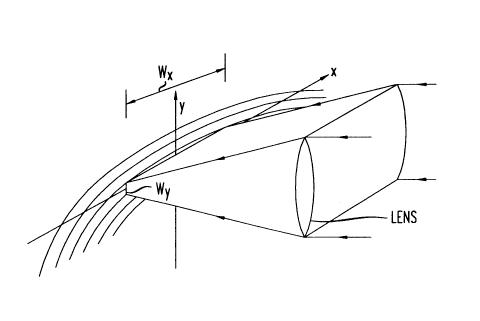
FIG. 2 shows one example of an irr~tliating arrangement in which a beam of
suitable radiation is transmitted through a lens. The beam scans along the transverse
direction, which in FIG. 2 is defined as the y direction. The lens focuses the radiation
beam so that the beam width Wy in the y-direction is appreciably smaller than the
5 beam width in the x-direction. In principle, the beam width Wy should be sufficiently
small so that a single waveguide and its immediately surrounding area may be
irradiated independently of adjacent waveguides. However, satisfactory results can
be achieved if the beam simultaneously irradiates a plurality of adjacent waveguides
that together compose a small fraction of the total number of waveguides in the
10 optical grating. For example, if M is the total number of waveguides in the grating
and W is the smallest spacing between adjacent waveguides, a suitable choice for the
beam width is Wy < (M/S)W. Factors to be considered in selecting an aL)prupfiatebeam width Wx will be discussed below.
The value of the compensating differential phase shift as imparted to a given
15 waveguide s of the grating by irradiation is approximately proportional to the beam
intensity, the effective length Ps of the waveguide s, and the total time ts over which
that length is irradiated. To ensure that the value of das is a constant for all s, a
compensating differential phase shift as must be imparted that increases in a
sequential manner from the first waveguide s = l to the last waveguide s = M (i.e., a2
2 0 = al + ~a~ a3 = al + 2~a7 etc.). Thus the irradiation time ts for the individual
waveguides must approximately increase linearly with s. Since in FIG. 2 s increases
in the direction of the coordinate y, this criteria amounts to requiring that the
irradiation time increase as the position of the beam increases in the y direction. If,
for instance, the waveguides are equally spaced,
t(Y)=ao+aly
where aO and al are suitable coefficients. If the irra~ ting beam scans along the
transverse direction with a velocity v(y), the irradiation time ts for a given waveguide
216~12
will be inversely proportional to the velocity v(y) at the location of waveguide s.
More particularly, t(y) = wx/V(y). Accordingly, the required irradiation time can be
expressed as follows:
t(y) ~y)=OCo+OClY (4)
Equation 4 assumes that the waveguides are equally spaced from one
another. This assumption may be removed by replacing the coordinate y in equation
4 with some function of y this is nonlinear with respect to s and which represents the
nonlinear separation between the waveguides. The above discussion also assumes
10 for simplicity that the beam scans continuously. However the above considerations
are equally applicable if the beam motion is discontinuous, i.e., if it proceeds in
discrete steps.
In practice, the effective length Ps of the waveguide s that is irradiated will
differ from waveguide to waveguide since the waveguides are in general curved (see
15 FIG. 1). As a result a correction factor must be introduced into the above expression
for the sc~nning time ts to account for the variation in Ps with s. The correction
factor can be calculated from the geometry of the optical grating in a straightforward
manner by recognizing that when the beam illumin~tes the central section of a given
waveguide it also illumin~tes the curved sections of nearby waveguides above the2 0 given waveguide. Thus, the correction factor may be determined by taking into
account this additional exposure that the waveguides receive before the beam
illumin~ttos its central section. However, the correction factor also may be
determined experimentally by initially exposing the device to an irr~ ting beam
having a scanning velocity given by equation (4) without any correction factor,
2 5 measuring the rem~ining polarization shift exhibited by the tr~ncmiscion spectrum of
the grating, and then calculating the additional irradiation necessary to elimin~te the
216571~
- 8
rem~ining polarization shift. For typical geometries, the required correction factor
will be small.
It was noted above that the beam width Wy in the transverse direction is
advantageously chosen to be sufficiently narrow to selectively irradiate only a small
5 number of adjacent waveguides at any given time. The beam width Wx in the x
direction (i.e., the direction more nearly parallel to the optical propagation direction)
typically must be larger than Wy. If the shortest waveguide in the optical grating is
denoted by s = 1 and is imparted with a compensating differential phase shift a1, then
the longest waveguide denoted by s = M must be imparted with a differential phase
10 shift aM equal to:
aM = (M - l)da + al (5)
This value of aM is necessary to ensure that as varies linearly with s for all s between
s = 1 and s = M. Since for most practical optical gratings M >10, the value of aM
will be generally much larger than a1. The effective length Ps of the waveguide that
15 is irradiated, and hence the width Wx of the beam, must be sufficiently large to
ensure that a comp~n~ting differential phase shift aM can be produced under
realistic irradiation conditions without the need for inducing large refractive index
changes. Of course, this analysis assumes that the irradiating beam scans solely in
the transverse direction. If the beam additionally scans in the orthogonal direction
2 0 (i.e., the x direction), then the width Wx of the beam in this direction can be reduced.
The above-described irradiation procedure for reducing birefringence is a
nondestructive and reversible process. That is, after irradiation the device may be
annealed to partially or completely elimin~ the compensating polarization shift that
results from the collective effects of the compensating dirrclcntial phase shifts, thus
2 5 returning the device to its original state. Consequently, the polarization shift due to
birefringence may be reduced or completely elimin~.d in a simple manner by firstoverexposing the device and then annealing it. For instance, by monitoring the decay
216S712
in the compensating polarization shift during the annealing step, annealing can be
termin:~tç~ when precisely the correct value has been achieved.
The optical grating must undergo an annealing process subsequent to the
irradiation process for an additional reason independent of that discussed above.
5 After the optical grating is irradiated the compensating polarization shift is found to
exhibit significant decay. However, the compensating polarization shift apparently
stabilizes after decaying approximately 10-20%. By extrapolating the decay data it is
anticipated that no additional decay will occur over the rem~ining lifetime of the
device (i.e., over twenty years). Thus, to provide a stable device at the outset the
10 initial decay can be accelerated by overexposing the device by 10-20% so that it is
overcompensated by an amount equal to the initial decay and then annealing it. By
choosing a suitable annealing t~mpe,dtul~, such as between 100-300C, for example,
the initial decay can be achieved in a reasonably short period of time, often in the
range of approximately 15 minutes. As a result, a device is realized in which
15 birefringence is reduced or elimin~te~l and which is stable immP~ tely upon
fabrication.
Moreover, rather than annealing the device after it has been irradiated, the
device may simultaneously undergo both the irradiation and annealing steps. If the
value of the compen.~:~ting polarization shift is monitored while the grating is being
2 0 irradiated and annealed, the procedure may be termin~t~ once the inherent
polarization shift has been elimin~te(l The resulting device will be stable without
undergoing any additional annealing. By performing the irradiation and annealingsteps simultaneously, the fabrication process is simplified and the total time required
is reduced. Moreover, once the various parameters such as exposure time, annealing
2 5 time and annealing telllpeldLure have been determined for one device, these same
parameters may be used to impart the requisite compensating polarization shift in all
other devices having identical configurations.
The method described above reduces or eliminates the inherent polarization
shift caused by birefringence which is observed in the transmission spectrum of an
2165~12
optical grating. The transmission spectrum exhibits other aberrations, however,
which are not caused by birefringence but which also may be elimin~ted by
irradiation. Such aberrations are caused by phase errors in the individual waveguides
of the grating typically due to imperfect manufacture. These aberrations manifest
5 themselves as distortions in the shape of the transmission function. Although the
aberrations are usually small, they can substantially increase the level of crosswalk
and distort the pass band. As noted earlier, irradiation induces phase shifts b5 and
b5 in the TE and TM modes respectively. Accordingly, irradiation may be used to
reduce or eliminate phase errors by selectively adjusting b5 and bs'' with radiation.
10 However, unlike the situation discussed above in which a substantial difference
between the induced phase shifts b5 and b5 was required to reduce the inherent
polarization shift, in the case of phase errors irradiation is ideally used to selectively
.. . ..
adjust b5 and b5 so that they are as nearly equal as possible. The reason b5 and b5
should be nearly equal to one another is because aberrations due to phase errors are
not in general strongly polarization dependent and therefore the selective adjustment
of the induced phase shifts b5 and b5 for the TE and TM modes, respectively,
should be approximately the same. For example, if the induced phase shifts satisfy
.,
the relation b5 > 2b5, phase errors in the TE mode may be completely elimin~ted
while only elimin~ting less than 50% of the phase errors in the TM mode.
2 0 The illustrative tr~n~mi~sion spectrum shown in FIG. 3 shows a main lobe
situated between two sidelobes. The sidelobes, which are undesirably large, are
primarily due to phase errors. Since the sidelobes are the result of phase errors they
are essentially symmetrically located about the main lobe with the same amplitudes.
This symmetry arises whenever the tr:~n.cml~.cion spectrum exhibits behavior primarily
2 5 caused by phase errors. In such cases any steps which are taken to correct the errors
on one side of the main lobe will also correct the errors on the other side of the main
lobe.
216~712
Due to competing factors it is not possible to completely elimin:~e both the
inherent polarization shift due to birefringence and aberrations due to phase errors.
When reducing the inherent polarization shift the compensating polarization shift
depends on the quantity as = b5 - b; . Accordingly the ratio r = b5 /b5 should be
5 appreciably greater than unity since otherwise large value of b5 will be required to
produce the requisite value of as. In contrast, as noted above, to correct aberrations
due to phase errors the ratio r should be close to unity. Therefore a value of r should
be chosen which represents a conl~lolllise between the two competing concerns. In
practice, a value of r between 2 and 3 has been found to be a reasonable
1 0 co~llplalllise.
It should be noted that the actual value of r depends in general on both the
exposure conditions and the router design and fabrication. In particular, r depends
on the strain distribution in the grating, which is often highly uniform in the vicinity
of the individual waveguides. Typically, for example, the top and bottom cladding
15 layers have different compositions and therefore highly nonuniform strain is produced
in the vicinity of the individual waveguides. As a consequence, the initial strain
before irradiation depends in general on both the composition of the top layers and
the core dimensions. Similarly, the inrl~lce~ birefringence can be highly nonuniform
since compaction induced by irradiation will also depend on the composition of the
2 0 top layers and the core dimensions. Therefore, it is possible to change the
..
coefficients b5 and b5 by properly modifying the core dimensions and the top
cladding composition in the central region of the grating.
To adequate!y remove aberrations due to phase errors it is sufficient to adjust
(by reducing or increasing) the TE transmission coefficient at or near selected
2 5 wavelengths. Therefore the phase shifts that must be induced will be the sum of a
series of components which each reduce a particular distortion component in the
shape of the transmission function, as discussed in C. Dragone, Optimal Finite-
Aperture Filters with Maximum Efficiency, Journal of the Optical Society of
216~712
America A, vol. 9, No. 11, pp. 2048-2055, 1992. The phase shift to be induced inthe individual waveguides of the optical grating will be of the form
oC cos [2~sa - b], a = ~ p (6)
where as before s denotes the individual waveguides constituting the optical grating
5 and it varies between 1 and M- 1, ~C is determined by the amplitude of the sidelobes
of the transmission function (see FIG. 3), ~1 is the difference between the center
wavelength of the main lobe and the center of the sidelobe, and ~p is the free spectral
range of the transmission spectrum. Of course, since the induced phase shift cannever be negative in value, a positive constant term must be added to expression 6 to
10 ensure that it is always positive-valued.
To achieve an induced phase shift that varies sinusoidally with respect to s, asrequired by expression 6, the irradiation time t(y) given by expression 4 must
approximately vary sinusoidally. Denoting by t(y) the sc~nning time required to
alleviate the effects of the inherent polarization shift due to birefringence and t'(y) the
15 sinusoidally-varying scanning time required to alleviate aberrations due to phase
errors, the actual scanning time tt(y) required to compensate for both types of
abérrations is the sum of the two time components:
tt(y) = t(y) + t'(y) (7)
FIG. 4(a) shows a graph of the sc~nning time t(y) that is required in the
2 0 special case where Ys is a linear function of s. As discussed earlier t(y) approximately
increases linearly as s increases. F~IG. 4(b) shows a graph of the sc~nning time tt(y)
which is required to compensate for both birefringence and phase errors. In
accordance with equations 6 and 7, tt(y)is approximately a linearly increasing
function of s on which a sinusoidal component is ~u~ælhl1posed. The value of angle b
2 5 in equation (6) may be experimentally determined by adjusting the phase of the
216~712
13
sinusoidal component seen in FIG. 4(b) until the optimal value of the angle b isreached which minimi7çs the amplitude of the sidelobes. In practice the optimal
angle b can be determined by ex~rnining two particular cases, namely, a scanningtime corresponding to b = O and a scanning time corresponding to b = tl/2.
It should be noted that the problems of reducing crosstalk and the problems
of reducing birefringence differ in several respects. First, the total exposure time is
typically smaller in the former case than in the latter since crosstalk is typically small.
Second, the former problem requires a higher resolution. In fact, to efficientlycorrect an aberration component corresponding to a given value of
U~ P
requires that Wy < W/4U l, where W is smallest spacing between the waveguides
along the y-axis. Therefore the required width Wy becomes small (close to W) when
4Ul is close to unity. Often, the most important aberrations are those close to the
main lobe of the transmission coefficient and, for these aberrations, the above
15 condition may not be difficult to satisfy. On the other hand, if 4U l is not small, then
it may be advantageous to accurately produce the required value of the beam width
by transmitting the irradiating beam through a slit of width Wy as shown in FIG. 6.
If this arrangement is used the relative motion between the irr~ ting beam and the
optical grating can be achieved by moving the optical grating while keeping the
2 0 irra liating beam and the slit fixed in position.
In view of differences between reducing birefringence and reducing crosstalk
it may be advantageous to employ different irradiation steps for each one. For
example, instead of irr~ ting the waveguides in a single scan, it may be desirable to
scan the waveguides two or more times, with each scan hnpa,ling a particular
2 5 correction.
An important parameter that affects the exposure efficiency is the fraction of
the total power from the irradiating source that is absorbed by the optical grating.
Typically, the absorption coefficient of silica varies with the wavelength of the
radiation and the particular composition of the silica. Generally, the absorbance is
2165712
-
14
relatively low. It may therefore be advantageous to increase the efficiency of the
method by employing multiple reflections from the slit shown in FIG. 5. That is, as
seen in FIG. 6, radiation transmitted through the slit, reflected off the grating and
then off the slit, may be subsequently absorbed by the waveguides.
S To improve exposure accuracy and simply the exposure conditions, a mask
101 such as shown in FIG. 7 may be employed. Of particular concern for most
applications are the first two sidelobes. In practice, it is often difficult to control the
fabrication process to the accuracy required to keep these two sidelobes lower than
the specified level. Thus the use of a mask may particularly significant to reduce
these sidelobes. The mask is designed to produce a pattern of exposed strips 103which are arranged so as to approximately produce the periodicity specificed by
equation 6. Each strip 103 is a transparent region that is approximately placed at one
of the maxima specified by equation 6. The desired compensation may be produced
by covering the waveguide with the mask and irr~di~ting the entire grating. Thus,
the mask can produce a periodic variation that approximates the sinusoidal induced
phase shift, as discussed above.