Note: Descriptions are shown in the official language in which they were submitted.
2 ~ 6 ~ 2
1 o
15 DECODER FOR AUDIO SIGNALS BELONGING TO COMPRESSED AND CODED
AUDIOVISUAL STREAMS
The present invention relates to processing systems for digitised audio and video
signals, and in particular its concerns a decoder for audio signals belonging to digital
2 0 audio-visual streams coded in accordance with the ISO/IEC 11172 (or ISO/MPEG-1)
standard. To keep the description simple, hereinafter reference shall be made to "MPEG
standard" and "MPEG streams".
The MPEG standard is a standard for the representation of compressed and coded
audio and video data, aimed at allowing a data exchange between compatible terminals
2 5 and at offering normalized decoding methodologies. The standard provides for an
organization of the compressed and coded data that is oriented to the transmission of
packets. The organization is hierarchical, whereby a higher level (system layer) entails
the transmission of a sequence of the so called audio-visual "packs", starting with a pack
start code and a pack end code; the sequence ends with transmission of a sequence end
3 0 code (ISO 11172 end code). An immediately lower level (pack layer) determines the
organization of the packs and prescribes that each of them comprises, after the start
code, timing information, the so-called system header and a number of audio and video
packets for one or more channels; each packet comprises a header with service
information, and the actual data. When decoding takes place, the different types of
3 5 packets present in a pack are demultiplexed and then decoded separately, by exploiting
the service information present in the packs (start code, synchronisation information and
system header) and in the packet headers.
CA 02166042 1999-03-24
~ 2
.
In the case of audio signals, which is the one of interest for the present invention,
the data inserted into the packets are organised into audio frames comprising a fixed
number of samples. Coding is a sub-band coding, the bit allocation to the different sub-
bands being determined on the basis of suitable human perception models. During the
S decoding phase, in addition to recovering the original audio signal, it is also necessary to
solve the problem of synchronisation with pictures belonging to the same transmission.
The problem is made particularly arduous by the fact that, according to the standard,
audio data can be sampled at a certain number of rates, in particular 32 kHz, 44.1 kHz
and 48 kHz, and the 44.1 kHz rate has no practically usable multiple in common with the
1 0 other two rates.
A commercially available MPEG audio decoder directly generates the clock signal
corresponding to the sampling rates of 32 and 48 kHz and obtains, from the latter, a
second clock signal, related to the 44.1 kHz sampling rate, through the use of an
accumulator which loads a fractional, user-programmable value, at each end-of-count of
1 5 the counter generating said clock signal and which adds 1 to the count in progress when
the accumulated value is more than one. This solution is not satisfactory because the
correction is very abrupt and it cannot be tolerated by the output digital-to-analog
converter, especially if the latter is of high quality. Moreover, the known device does not
include any means for recovering possible phase shifts between the timing indications
2 0 associated with the data stream (based on the clock signals generated by the encoder)
and the clock signal generated by the decoder.
According to the invention, an audio decoder is provided instead wherein the
correction of the second clock signal, too, is managed directly by the decoder, with no
need to use extemal devices, and is performed in a smooth manner, and wherein,
2 5 moreover, means are provided to recover any possible phase shift between the timing
indications associated with the data stream and the clock signals generated by the
decoder.
The characteristics of the invention are reported in the claims which follow.
For the sake of greater clarity, reference is made to the enclosed drawings, wherein:
3 0 - Figure 1 is an outline of an MPEG decoder;
- Figure 2 is a diagram of the structure of the packets and the frames;
- Figure 3 is a functional block diagram of the audio decoder of the present invention;
- Figures 4, 5 are block diagrams of the circuit managing audio-video synchronisation;
- Figures 6A and 6B are state diagrams of a logic of the circuit for managing audio-video
3 5 synchronism;
- Figure 7 is a state diagram of the circuit for synchronism search and verification;
- Figure 8 is a block diagram of the presentation unit; and
- Figures 9A, 9B are time diagrams of some signals generated by the presentation unit.
2 1 6~0i~Z
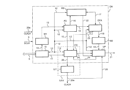
As can be seen in Figure 1, a decoder DMP for decoding audio-visual streams
encoded in accordance with the MPEG standard comprises, in principle, a system
decoder DS, which receives these streams from a source SA (for instance a remoteencoder) and demultiplexes them into the audio and video streams which are sent, still in
5 coded form, to respective decoders DA, DV, as represented schematically by
connections 1, 2. System decoder DS supplies DA, DV with timing information as well,
as represented by connection 3. Decoder DMP is associated with a controller CN which
is to program and supervise the various components of DMP (connection 4) and canalso carry out the functions of DS. For the sake of clarity, however, the drawing
10 represents separate units for system decoding and component programming/
supervision. The decoded streams are then sent to audio and video terminals TA, TV.
Audio decoder DA, which constitutes the subject matter of the present invention, is
able to decode monophonic and stereophonic audio signals compressed in the formats
prescribed by the so-called audio layers I and ll of the standard. Decoder DA is an
1 5 integrated-circuit component which receives the coded audio streams and configuration
data through a parallel bus which advantageously, with regard to data, can be
configured by the user as 8 bit or 16 bit bus; through the same bus, the decodertransmits state information to the controller. Decoded audio signals are emitted in PCM
serial format at a number of sampling rates, in particular 32 kHz, 44.1 kHz and 48 kHz. In
2 0 addition to carrying out decoding functions, DA also manages recovery from possible
error situations in the data streams and it also manages the synchronism of the emitted
audio signals with the associated video signals. Through a command word it is also
possible to force a global reset of the device initial conditions.
The structure of DA is represented in greater detail in Figure 3. To ease
2 5 understanding of the invention, before describing that structure, the organization of an
MPEG pack shall be briefly illustrated, with reference to Figure 2.
An MPEG audio-visual packs comprises service information (here represented in
the whole by a Pack Layer Header PLH and by a System Header SH, which is
optional) and a sequence of packets PKT1, PKT2...PKTn. As shown for PKT1, each
3 0 packet is formed by a packet header PHD and by a certain number of data bytes PDA.
Header PDH comprises, in case of audio packets:
- 3 bytes PSC constituting the packet start code, which is used to identify packet
synchronism;
- 1 byte SID encoding the identity of the stream to which the packet belongs;
3 5 - 2 bytes PL encoding the packet length;
- a variable number of bytes HDA, some of which are stuffing bytes used when thesampling rate is 44.1 kHz and possibly when the data are in free format (i.e. when the
transmission occurs at a different bit rate from those defined by the standard and
4 2 1 ~Oi4 2
_
-
lower than a maximum rate admitted for the adopted coding modes) and others contain
service information of no interest for the invention;
- a group of bytes TS intended to contain possible timing indications, i.e.: no indication;
the presentation time stamp PTS; or the presentation time stamp and the decoding5 time stamp DTS; the number of these bytes depends on the indications transmitted;
in the preferred realization of the invention, time stamp DTS, though present in the
data stream, is not utilised.
The packet data bytes are in turn inserted into fixed-length frames (made up of 384
samples for the so-called coding layer I and of 1 152 samples, i.e. 384x3, for coding layer
1 0 11); only one frame, FRi, is indicated in the figure. The frames comprise:
- a header (FHD) composed of a synchronism word SYW and of a control word CW
specifying coding level, type of audio stream (stereo/mono), bit rate, sampling rate,
emphasis (if any), tables for bit allocation to the sub-bands and information on scale
factors;
1 5 - audio samples AUS;
- possibly, a word CRC for error detection and user-defined ancillary data AND, for
example subtitles for the video part.
It must be specified that the organization into frames is independent of the
organization into packets and that a frame can span successive packets. In this case, if
2 0 TS (Figure 2) contains a stamp PTS, the latter is related to the first frame starting in the
packet.
Figure 3 illustrates a functional block diagram of the decoder according to the
invention. To keep the drawing simple, the various inpuVoutput signals of the
component or the signals exchanged between the various units have not been
2 5 indicated. Signals of interest for the invention shall be come evident further on in the
description.
Decoder DA is connected to bus 5 (which corresponds to the set of connections 1
and 4 in Figure 1 ) through a system interface IS, which is a conventional microprocessor
interface managing the dialogue of the device with the outside and the device
3 0 programming. IS receives audio packets and synchronisation information (in particular,
system clock signal SCLK) from DS (Figure 1) and programming information from CN; IS
also transfers information on the state of the other circuits in the decoder to controller CN.
Dialogue with the outside through bus 5 occurs with the use of totally conventional
protocols.
3 5 Through programming registers contained in IS, it is possible to control:
- format of input and output data;
- output data oversampling factor (data can be emitted in base band, i.e. without
oversampling, or oversampled by a factor 2, 4, 8);
2 1 ~6~42
- selection of the input audio data stream;
- enabling/disabling audio data output;
- parameters and data format of the circuits for managing audio-video synchronism,
described further on.
IS can generate interrupt signals INTR in response to events signalled by the
circuits in the device, in particular:
- recognition of a PTS stamp in the incoming data flow;
- synchronism errors;
- starting the presentation of output data;
1 0 - locking on to the incoming data strearn synchronism;
- impossibility of recovering phase shifts, or error conditions in the presentation unit
and/or in the unit for synchronism search and verification.
Other information which can be accessed externally is:
- the control word of the last decoded frame;
1 5 - the value of the last PTS stamp extracted from the data stream;
- indications on the state of some of the internal circuits.
Through a connection 10 IS supplies an input buffer memory M1 audio data to be
decoded and, through a connection 11, it supplies device SAV, managing audio-video
synchronism, with the so-called "system clock reference", SCR, which is computed by
2 0 an internal counter controlled by the system clock signal SCLK and is used to generate
and correct audio-video synchronisation signals. Interface IS also provides the other
units of the device with control signals, which do not require detailed discussion, and
receives therefrom state information to be made available to the outside. Line 12 outlines
the connections between IS and the other units of the device for the exchange of2 5 command signals or state information.
Memory M1 is to compensate any variation in input data rate and to supply, data
in the format determined by downstream units. Through a connection 13, memory M1supplies audio data to an audio packet parser AS, which recognises constructionsbelonging to the "audio packet" layer of the standard and extracts from them information
3 0 of significance for the decoding process. In other words, AS must recognise the service
bytes contained in the packet headers: since the configurations and the sequence of
these bytes are defined by the standard, the structure of a logic network which carries
out such recognition is implicitly defined by the standard and therefore a detailed
description of AS is not necessary.
3 5 AS emits, on a connection 14, the "net" data (i.e. without service information),
which are transferred downstream only after presentation time stamp PTS has beenidentified; until that moment, these data are discarded since no presentation time can be
associated with them. Presentation time stamp PTS is also supplied to the circuits
21 6~0iL2'
managing audio-video synchronism SAV (connection 15) and its presence is also
signalled along the decoding chain, synchronously with the data to which it refers.
In the presence of events preventing correct recognition of the service byte
sequence, for example errors in the packet structure or in the stream identifier, AS
5 generates and sends to a synchronism search and verification circuit RS, through a
connection 16, a signal which is utilised to stop emission of the output data stream.
The data are passed from AS to the audio stream decoder DFA which carries out
operations required by the "audio" !ayer of the standard. In particular, in DFA the
synchronism word present at the start of each audio frame is recognized; the frame
1 0 header is decoded and information of relevance for the decoding process (control word,
allocation tables, sample scale factor tables) is extracted from such header; if the header
is protected, its integrity is checked; audio data contained in the frame are decompressed,
re-quantified and re-scaled; then, the conversion from the frequency domain to the time
domain and the windowing, prescribed by the standard, are carried out. Moreover, any
1 5 ancillary data present in the frame after the audio data are discarded. For its operations,
DFA is associated with a working memory, which is not represented.
Regarding decoding, it is not necessary to provide additional details, which can be
found in the text of the standard and in particular in part 3 of the same (ISO/IEC 1 1172-
3), where the flowcharts of the decoding operation are reported.
2 0 DFA provides the synchronism search and verification unit RS with information on
the acquisition or loss of the frame synchronism (connection 17) and receives, in
response, information governing the evolution of the decoding operations. Data decoded
by DFA are supplied, through a connection 18, to a presentation buffer M2, for instance
organised by pages, in a way which depends on the coding layer and on the type of
25 audio stream. The data are transferred, through a connection 19, from M2 to apresentation unit UP which manages the serialisation and the presentation, through a
connection 21, of the decoded audio samples. Serial data can be emitted in the "two's
complement" or "offset binary" formats, in base band or oversampled by a factor 2, 4 or
8, depending on the component programming. Unit UP also produces a signal BCLK
3 0 (discussed in connection with Fig. 8) which indicates the sampling instant of the output
data. UP will emit mute frames either in the presence, on connection 12, of a signal which
IS derives from the programming information it contains (muting function), or in periods set
by unit RS, which supplies the necessary information through a connection 22.
The synchronism search and verification unit RS manages the search for
3 5 synchronism in the incoming data stream and its recovery in case of errors or
interruptions in the stream. Based on information provided by AS and DFA, the
correctness of the distance between successive synchronism words is checked. In case
of free-format data, the unit also identifies the length of the frame used. Through system
- 2 1 66042 ~,_ 7
-
interface IS, the unit signals to the outside both the identification of the synchronism and
any synchronism errors which may be present. The operations of RS shall be described
in more details with reference to Figure 7.
Audio-video synchronisation managing unit SAV is to:
5 - start data presentation, by comparing the system clock reference SCR and the device
internal time, evaluated indirectly through the instant of presentation of data which are
associated with an indicator PTS supplied by AS; the start-of-presentation command
is supplied to UP through wire 24;
- generate a timing signal (CLK24) for the different circuits in DA; such signal is supplied
1 0 to said circuits through a wire 20a;
- control, through a suitable feedback circuit FD comprising a digital filter, the data
presentation rate, in order to minimize the difference between SCR and the internal
time; any discrepancy between SCR and internal time exceeding the operating range
of the digital filter causes filtering to be suspended and it is signalled to the controller
1 5 through IS; the presentation timing signals are supplied to UP through a connection
20, of which said wire 20a is part.
Maintaining presentation frequency and internal time locked to the correspondingsystem values guarantees synchronisation between the audio data being emitted and
the associated pictures. For its operations, SAV needs information contained in the
2 0 control word CW, which information is supplied to SAV by DFA through connection 23.
Block SAV essentially consists of two parts: correction unit FD and units GT
actually generating the timing signals; the latter units are outside the integrated circuit DA,
enclosed within the dotted and dashed line. To keep the drawing simple, the wires and
connections which bring signals SCLK and CLK24 end at the border of the integrated
2 5 circuit, and they are not brought to all the units that utilise them. Again for the sake of
simplicity, the signals for memory addressing and command are not indicated, since they
are not of interest for the invention.
The structure of block SAV shall now be described in further detail, with reference
to Figures 4 - 6.
3 0 As previously stated, according to the standard the audio data can be sampled
either at a first rate of 48 or 32 kHz (which in the invention is derived from a frequency of
24.576 MHz) or with a second rate of 44.1 kHz (derived from a frequency of 22.5958
MHz). Depending on the sampling rate utilised, data presentation is controlled by either
of two clock signals CLK24, CLK22 which are generated by block GT, which is
3 5 essentially a digital phase locked loop with a pair of digital-to-analog converters DAC1,
DAC2 and a pair of voltage-controlled oscillators VC01, VC02 which generate the two
signals CLK24, CLK22. Signal CLK24 also constitutes the timing signal for the other
units in DA and therefore it is supplied to them irrespective of the output data sampling
8 2 1 66Q42
rate; however, check and correction of CLK24 by FD are carried out only if the output
data sampling rate is 32 or 48 kHz.
This stated, an input counter CN1 counts, upon command of the system clock
signal SCLK, signals SCR supplied by IS and supplies the value of the count to the
5 positive input of a subtractor ST1, which subtracts from this value the value PTS of the
presentation time stamp, supplied by parser AS (Figure 3) through connection 15 and
hold in a register R1. ST1 also receives at an additional subtraction input a signal DIFFB
representing a fixed numeric value (in practice, a signal representing a unit value): that
signal compensates the fact that the difference SCR - PTS is calculated with a delay of
1 0 one period of SCLK, to enable the circuit to lock the various signals needed for operation,
which arrive asynchronously, to SCLK. Output DIFF of ST1 is supplied, through a
connection 27, to a digital filter FN, which is a filter whose zeros, poles, gain and output
data format can be programmed through system interface IS (Figure 3). If the difference
SCR - PTS is within pre-set limits, filter FN generates, on output 24, the presentation
15 start signal, and, on a group of wires of connection 26, a correction signal which,
converted into an analog signal by either of two digital-to-analog converters DAC1,
DAC2 depending on the chosen presentation frequency, is used to drive oscillatorVC01 or respectively VC02. On another group of wires of connection 26, FN supplies
the commands for selecting one of the converters. FN is enabled to emit the correction
2 0 signal by the presentation unit UP, through connection 25, when UP recognises a time
stamp PTS.
Note that, when the data presentation rate is 44.1 kHz and therefore signal CLK24
is not to be corrected, converter DAC1 will continue to emit a value set in the course of
the device initialisation phase, for example the value corresponding to the central value
2 5 of the admitted interval for the difference SCR - PTS (hereinafter referred to also as
"central value of the filter band").
Figure 5 shows that digital filter FN comprises an operating unit UOF (i.e. a unit
which implements the filter transfer function), a logic network LC1 controlling the operating
unit and a logic network LC2 for the management of external signals. Both logic networks
3 0 are made up of a finite state machine.
Operating unit UOF comprises a multiplier ML1 which receives from ST1 (Figure 4~the difference signal DIFF and multiplies it by gain G supplied through wires 12a of
connection 12, giving a signal DIFFG. Gain G can have a limited number of discrete
values (e.g. 2, 4, 8) and multiplier ML1 is advantageously implemented by means of a
3 5 shifting combinatory logic. Signal DIFFG is added, in an adder SM1, to a signal RP which
is the output signal of a divider DV1 which divides the output signal of the filter memory
register RM by the value P of the pole (present on wires 12b of connection 12). The
pole, too, can only have a limited number of discrete values, and divider DV1 also is
- 2 1 ~0~2
.. ~ g
advantageously implemented by means of a shifting combinatory logic. The output
signal of RM is also divided, in a second divider DV2 analogous to DV1, by value Z of
the filter zero, present on wires 12c. The output signal of DV2 is then subtracted, in a
subtractor ST2, frorn the output signal of SM1, giving filtered signal OUT.
The filtered signal OUT is stored in an output register RU which supplies, over
wires 26a of connection 26, the value VF to be loaded into the involved converter DAC;
the most significant bit of signal VF is combined, in an exclusive OR gate PX, with a
signal VFOB which is supplied by the controller through interface IS and wires 12e and
which indicates the data output format: offset binary format if VFOB = 1, or two's
10 complement, if VFOB = O. Moreover, during the initialisation phase, a value of VF
corresponding to the central value of the filter band is set in the filter output register RU.
Loading commands for the memory register and the output register are representedby a signal CK, emitted by LC1. The precise time relations between the different events
are not of interest for the invention.
Figure 6 represents the state diagram of LC1. In the filter working cycle, the
following phases can be identified:
- resetting DAC1, DAC2 and VC01, VC02;
- waiting for timing references SCR, PTS;
- synchronising with SCLK and checking that the difference between SCR and PTS
2 0 lies within a pre-set interval;
- generating the presentation start signal (START);
- waiting for PTS from the presentation unit;
- actual filtering.
More in particular, in an initial state VCO_RST of the filter, logic network LC12 5 selects one of the converters and the corresponding oscillator (e.g. DAL1, VC01, signal
IVSEL=1), subtracts the value 1 from the difference between SCR and PTS (DIFFB=1)
and goes to state VCO_RST1 where DAC1, VC01 are reset. For the reset, LC1 asks
LC2 (WRVFOUT=1 ) to write the central value of the filter band into the converter, which
value is stored in RU (Figure 5). LC1 remains in state VCO_RST1 until it receives from
3 0 LC2 a signal confirming that reset has occurred (WRVFRDY=1), after which it goes to
state VCO_RST2 (IVSEL=O) of reset of DAC2, VC02. Operations carried out in
VCO_RST2 are identical to those carried out in VOC_RST1. When the new confirmation
arrives from LC2, LC1 goes to a state of wait for SCR, PTS (state VCO_WAITSP).
In this state, the converter and the oscillator corresponding to the desired sampling
3 5 frequency (information contained in control word CW) are enabled by setting IVSEL to
the appropriate value, and the arrival of flags indicating a valid SCR and a valid PTS
(SFLAG, PFLAG) is awaited. These flags are supplied by the same units which supply
SCR and PTS (thus by IS and AS) through wires 11b, 15b of connections 11, 15, and
2 1 66~42
_ o
are stored in respective registers (SFLAG_R, PFLAG_R). When both a valid SCR and a
valid PTS are recognized (SFLAG_R ~ PFLAG_R = 1), LC1 passes to the phase of
synchronisation with the system clock and verification of the difference between SCR
and PTS.
In the first state of this phase (VCO_SCLK1), a pulse of SCLK is awaited and,
when it arrives, a state VCO_STCHK is attained, where the difference between SCRand PTS is checked. For the system to function correctly the condition PTS-~1 ~ SCR <
PTS (condition indicated hereinafter as SCR ~ PTS) should be verified, but the filter is
able to recover even situations in which PTS ~ SCR ~ PTS+~2. If SCR ,, PTS (i.e. if
1 0 SCR - PTS > ~2), error state VCO_ESTART is attained, where, an error signal ERROR
is sent to interface IS (Figure 3) and SFLG_R is set to zero. Signal error is presented on
wire 1 2d (Figure 5) of connection 12. Error state is left due to an external intervention, for
example the arrival of a new SCR.
If SCR < PTS or SCR < PTS+~2, the generation phase of signal START is
15 entered. More particularly, if SCR < PTS, logic network LC1 goes into state
VCO_START, which is a state of data presentation enabling, in which a preliminary
synchronisation of presentation unit UP (Figure 3) with the filter is carried out. Logic LC1
leaves this state when SCR=PTS and SCLK=1: the START signal for UP is generated
and presented on output 24 (Figure 5) and LC1 goes on to state VCO_FILT, which
2 0 represents the normal filtering cycle: here, a filtering cycle is carried out, generally an idle
one because no corrections are needed. Then LC1 moves to state VCO_WPTS,
awaiting the next PTS. If PTS ~ SCR < PTS+~2, signal START is immediately
generated and LC1 moves directly to state VCO_WPTS. Here DIFFB is set to 0 and
LC1, waits for UP to communicate that the moment to carry out filtering has come2 5 (PTSPU=1), i.e. waits for UP to supply a PTS signal through connection 25.
When this signal arrives, LC1 passes to state VCO_FILT, where three situations
can occur:
a) the difference between SCR and PTS has a value Iying within a range ~ (~ = ~1+~2)
which can be recovered by the filter: filtering is carried out by loading the computed
3 0 values DIFFG+RP, OUT into the memory register RM (Fig. 5and respectively the output register of the filter and LC1 moves back to state VCO_WPTS;
b) if SCR << PTS (i.e. SCR < PTS-~1), the signal START is set to 0, thereby
suspending presentation of the output data and LC1 returns to state VCO_START;
c) if SCR >> PTS, the error signal is generated and LC1 returns to waiting state3 5 VCO_WPTS.
Logic LC2 is essentially to emit on wires 26b (Figure 5): a signal VFSEL for
selecting converter DAC1 or DAC2, on the basis of command IVSEL supplied by LC1; a
signal VFCSN to enable the converter; and a signal VFWRN to command loading, into
2 t 66042
1 1
the selected converter, value VF present on output 26a of register RU, on the basis of
command WRVFOUT emitted by LC1. LC2 will also supply LC1 with a signal WRVFR
upon conclusion of the operation. The realization of a logic network carrying out these
operations is not a problem for the skilled in the art.
Figure 7 shows the state diagram of the synchronism search and verification unitRS. Given the diagram, the skilled in the art has no problem in realising the logic network
which operates according to the same. For sake of clarity, the drawing shows only those
conditions which determine certain transitions, whilst operations carried out in the various
states or during the transitions are reported in Appendix I enclosed. There, like in
10 Appendix ll which shall be described further on, the transitions that do not bring about
any action are not reported. In the diagram, as well as in the appendices, symbols !, &,
indicate logic conditions NOT, AND, OR respectively.
Unit RS is a logic network which manages a group of counters and is essentially
to:
1 5 - determine the number of bytes contained in a frame being processed, in the case of
free-format stream (in the case of fixed format, the number is written in each frame
header);
- verify that the distance between two successive synchronism words is correct (i.e.
verifying that synchronism has been reached and maintained);
20 - compute the number of frames elapsed between the start of the stream and
synchronism lock-on (i.e. the number of frames which are not to be forwarded to the
presentation unit).
Initial state RST is a state of reset of all registers and counters in RS. These are:
- BIT_REG = register which stores the count of the number of bits in a byte;
2 5 - BYTE_CNT = counter of the number of bytes in the frame;
- FLAG_REG = register which stores a flag indicating the end of count of the number of
bytes;
- GLOB_CNT = counter of the number of words after a PTS;
- LDNMUTES_REG = register which stores a flag indicating the end of count of the3 0 number of bytes to be suppressed;
- NBYTES_REG: register which stores the number of bytes in the frame;
- NMUTES_REG: register which stores the count of the number of bytes to be
suppressed;
- SYNC_REG: register which stores a flag of synchronism identification;
3 5 - SYNCLOST_REG: register which stores a synchronism loss flag.
Note that for all aforesaid registers/counters, except GLOB_CNT, reset consists in
forcing a value 0, whilst for GLOB_CNT a negative value (e.g. -2) is forced to take into
21 ~0~2
''_ 1 2
account the fact that a number of counting cycles is lost in the initial working phases of
the machine and to cause the count to actually start after the arrival of stamps PTS.
State RST can be reached from all other states of the machine (transition 0) in case
of error or loss of packet synchronism (signal PSYNCL) communicated by AS (Figure 3).
5 If this transition occurs, the synchronism loss flag is set to 1 and stored inSYNCLOST_REG.
From state RST, the machine moves on to state START, awaiting identification of
the synchronism word (SYNC_IN). In this state, counter GLOB_CNT starts counting the
bytes after PTS. If PTS arrives before a SYNC_IN, state START is related to this new
1 0 PTS and therefore global counter GLOB_CNT is reset to value -2. This operation is also
repeated in the subsequent states. When SYNC_IN arrives, the next state (HEADER)is attained where a valid frame header (signal LDHEAD supplied by DFA) is awaited. In
the course of the transition (Transition 3), counter BYTE_CNT is reset and value NBITS
of the bit count within the byte is stored in BIT_REG, in order to recognise synchronism
1 5 at the bit level in the following frame. In state HEADER, counter GLOB_CNT is treated
as before and in addition the bits BSTART, signalling the start of a byte to increase byte
counter BYTE_CNT, are counted.
When LDHEAD arrives, RS leaves state HEADER and goes on to state FINDFMT
where the frame format is examined. In the course of the transition, output
2 0 HD_DEC_LOGIC(CW) of a decoding logic of control word CW, is loaded into register
NBYTES_REG: such output is a number indicating a free format frame (f_f in the figure) if
its value is 0 and corresponding the number of bytes in the frame if its value is different
from 0.
RS leaves state FINDFMT, moving on to synchronism check state SYNCCHK, if
2 5 the frame is a fixed frame (f _f ) or, in the case of a free format frame, when the frame
length has been identified, i.e. when synchronism lock-on has been attained at the bit
level, which is indicated in the Figure by a_s_in (transitions 8). In the case of free format
frame, the value of BYTE_CNT less the number of padding bytes PADBYTES is loadedinto NBYTES_REG and BYTE_CNT is set to zero. If a bit BSTART arrives, state
3 0 ENDFMT can be reached, because this bit is to be counted only in the subsequent
frame. In the course of this transition, too, the aforesaid operations, related to
BYTE_CNT, are carried out. In state ENDFMT, counter BYTE_CNT is increased.
State SYNCCHK is the normal working state of the logic. In this state, the end of
the count of the bytes in the frame (e_o_c) is awaited, together with the arrival of the
3 5 next frame synchronism byte (signal SYNC_IN supplied by DFA). Upon the arrival of
e_o_c, a value 1 is loaded into a register (FLAG_REG) just tasked with storing such an
event. When both e_o_c and SYNC_IN have arrived, synchronism lock-on for the
current frame (SYNCOUT = 1 ) is indicated. If this is the first lock-on, RS passes to state
2 1 66042
_ 13
NMUTES, where the number of mute frames to be emitted is determined and is signal to
the presentation unit (connection 22 in Figure 3). This number is obviously given by the
value counted by GLOB_CNT divided by the number of bytes in the frame. If it is not
the first lock-on (SYNC_REG=1), the machine remains in state SYNCCHK (transition5 10a).
If a bit BSTART arrives while the logic is cycling in state SYNCCHK, state
ENDCHK is reached, which is left without any condition.
If the end-of-count has arrived, but SYNC_IN has not, this can mean that the
upstream unit which supplies the data is busy: the machine remains in state SYNCCHK
1 0 (transition 1 Ob). This state is left either because the first SYNC_IN arrives (passage to
NMUTES) or because SYNC_IN has not arrived, but a new byte (e_o_c) has. If this
second case occurs, then synchronism has been lost: if in the previous frames
synchronism lock-on had already been attained, the machine moves on to state RST,
storing the event in register SYNCLOST_REG, otherwise it moves on to state START.
1 5 Figure 8 depicts the structure of presentation unit UP (Figure 3). This comprises: a
data presentation register RPD, for the serial emission of output data; a logic network
LC3 managing the unit and a logic network LC4 generating control signals for LC3. The
operations of the circuits in UP are timed by signal CLK22 or CLK24, depending on data
sampling rate.
2 0 Register RPD is a shift register (e.g. with 16 positions, if data are emitted as 16 bit
words) operating as a parallel-to-serial converter. Since a datum has to be presented in
output only once, or 2, 4 or 8 times depending on the oversampling factor, the register
shall advantageously be of the cyclical type, to avoid having to reload the datum each
time.
2 5 Logic LC3 controls the data loading into RPD and their emission over wires 21 a of
connection 21 by RPD on the basis of the signals received from LC4; moreover, again
on the basis of the signals received from LC4, it emits over a wire 21 b the command WS
to change channel at the end of each word emitted, and over a wire 21 c the signal BCLK,
representative of the correct instant in which output data are taken by downstream units.
3 0 Instead of data, LC3 will command the emission of mute frames, composed for instance
of the centre-range value, if the muting signal MUTE, supplied by IS through wires 12f of
connection 12, is active, or for the number of frames determined by signal NMUTES
present on connection 22.
Logic LC4 is to obtain, from the count value of a 7-bit down-counter DCNT, signals
3 5 LD, SHIFT, TWS which allow the management network LC3 to command data loading
and data shift in register RPD and the presentation channel switching. These signals are
generated on the basis of the output data oversampling factor set during the
2 1 66042
~_ 1 4
programming phase (signal OSFAC, which is supplied by IS over wires 1 2g and which
can take on the value of 1, 2, 4 or 8). In particular:
a) in the case of oversampling by a factor 8, wherein 128 bits are emitted (one every
counting step of DCNT):
- signal SHIFT is active throughout the counting cycle of DCNT (from 127 to 0);
- commands TWS and LD are generated when DCNT has reached value 1, i.e. in
correspondence with the next to the last bit (with reference to the output
signals);
b) in case of oversampling by a factor 4, wherein 64 bits are emitted (one every other
10 counting step of DCNT):
- signal SHIFT is activated every other step of the count of DCNT;
- command TWS is still generated in correspondence with the next to the last bit to
be emitted, and therefore when DCNT has reached a value of 2;
- command LD is generated when DCNT has reached a value 1.
1 5 The same principle is adopted in the case of oversampling factors 2 and 1: shifting
shall occur every 4 (8) steps of the count of DCNT; TWS is emitted in correspondence
with the next to the last bit (and therefore when DCNT counts 4 or 8 respectively) and
LD is always generated when DCNT has reached a value of 1.
The signals emitted by LC4 in the case of oversampling factor 8 and 4 are also
2 0 depicted in the diagrams in Figures 9A, 9B: for the sake of completeness, Figure 9A also
indicates signal WS and the bits outgoing from RPD.
The skilled in the art has no problem in realising a logic operating in the aforesaid
manner: it is evident that in practice, when the three most significant bits of the count of
DCNT are 0, it shall be sufficient to carry out the AND operation between the value of
2 5 OSFAC and the three least significant bits of the count of DCNT to generate LD, and the
EX-OR operation between the value of OSFAC and the four least significant bits of the
count of DCNT to generate TWS.
Management unit LC3 is a state machine presenting four working states: WAIT,
MUTE, SKIP, ACTIVE, plus a loading state (WLOAD, MLOAD, SLOAD, LOAD) for
3 0 each of them.
State WAIT is a state where the start of the presentation is awaited. In that state,
unit UP emits mute signals corresponding with silence and awaits the arrival of a loading
command LD. When the latter arrives, a check is made to see whether mute signals have
been emitted on the two channels (signal CH) and whether the START signal has
3 5 arrived. If both START and CH have arrived, the logic checks the availability of the
number NMUTES of mute frames to be emitted to take into account the time elapsed to
recognise PTS. This information is communicated by unit RS (Figure 3) by means of a
signal LDNMUTES transmitted on connection 22 which also carries value NMUTES to
1 5 2 1 66(~4~
-
UP. If LDNMUTES is present and the number NMUTES is different from 0, the machine
moves on to state MLOAD and then to state MUTE, which is the state where mute
frames are emitted. The transition is carried out if data are present in memory M3 (Figure
3). This is indicated by a signal DRGNT. If NMUTES is 0, the machine moves on to5 state WLOAD or LOAD depending on whether or not an external mute signal, MUTE,supplied by IS, is present (Figure 3). If signal LDNMUTES is not present, the machine
goes on (through SLOAD) to state SKIP which is similar to WAIT and which shall be
examined further on in the description. The same transition is carried out if data are not
available (DRGNT).
1 0 In state MUTE, the emitted frames are counted backwards until NMUTES is equal
to 0. From state MUTE, UP moves to state SKIP (through SLOAD) if no samples
(DRGNT) are available when emission of these frames is completed. If samples areavailable, the machine goes back to waiting state WAIT (through WLOAD) if an extemal
muting signal MUTE is active, otherwise it moves on to state ACTIVE through state
1 5 LOAD.
In state ACTIVE, signal samples are emitted by regularly alternating data loading
and emission for the right and left channel, in case of stereophonic transmission, and
loading and emitting the same datum on both channels for a monophonic transmission. If,
in this state, a lack of data occurs, the machine moves on to state SKIP and, if signal
2 0 MUTE becomes active, the machine moves to state WAIT, as has already been stated
for state MUTE.
Finally, state SKIP is a synchronism-maintenance state, where the machine goes if
data to be forwarded lack. In this state, mute frames are emitted, taking into account,
however, that each frame replaces a datum; therefore, when data become available, the
2 5 number of frames to be emitted shall have to be reduced as a consequence.
The operation described above is also illustrated in Appendix ll which reports the
table of the states and the list of actions to be carried out for each state and transition.
The state diagram has not been depicted graphically because, given the high number of
possibilities of transitions from one state to another, it would have been practically
3 0 incomprehensible. With reference to the appendix itself, some comments are appropriate
to highlight correlations with Figure 8 and to explain some actions. In particular:
- the terms: DATASR; ROL(DATASR) respectively indicate register RPD and the
cyclical bit shift within it;
- RDYMUTES indicates the availability of the aforesaid value NMUTES;
3 5 - SKIP_CNT indicates a counter of the number of samples used in state SKIP
- SAMPLES_CNT indicates a down counter of the number of samples of a frame
emitted on each channel. The reader is reminded that each frame comprises 384
samples for layer I (indicated by signal LAY12) and 1152 (i.e. 3x384) in layer ll, and
~ ' 16 21 ~0'42
therefore the counter shall be initialised at value 383: taking this into account, the
conditions related to LAYl2 in transitions 5, 14, 19, 30 indicate that the blocks of 384
samples are counted twice for a stereo transmission and once for a monophonic
transmission for layer I and respectively 6 and 3 times in case of layer ll;
5 - OB is the signal which indicates the format of output data (corresponding to VFOB in
Figure 5);
- PTSF is a signal (associated to data supplied by M3, Figure 3) which indicates that
the datum emitted is associated to a PTS stamp and therefore that device SAV canstart functioning.
It is evident that what has been described is provided solely by way of non-
limiting example, and that variations and modifications are possible without departing
from the scope of the invention.
17 21 66~4~
'_
APPENDIX I
(OPERATIONS OF RS. see FIG. 7)
(0) SYNCLOST_REG ~1
5 RST BIT_REG ~ 0; BYTE_CNT ~ 0; FLAG_REG ~ 0; GLOB_CNT ~ -2;
LDNMUTES_REG ~ 0; NBYTES_REG ~ 0; NMUTES_REG ~ 0;
SYNC_REG ~ 0; SYNCLOST_REG ~ 0;
START: if START PPPTS ~ GLOB_CNT ~ -2; else if BSTART ~ GLOB_CNT
~ GLOB_CNT + 1
10 (3) BYTE_CNT ~ 0; BIT_REG ~ NBITS
HEADER: SYNCOUT ~1 ;
if STA~T PPPTS ~ GLOB_CNT ~ -2; else if BSTART ~ GLOB_CNT
GLOB_CNT + 1; if BSTART ~ BYTE_CNT ~ BYTE_CNT + 1;
(5) NBYTES~ HD_DEC_LOGIC(CW);
15 FINDFMT: if START PPPTS ~ GLOB_CNT ~ -2; else if BSTART ~ GLOB_CNT
~ GLOB_CNT + 1; if BSTART ~ BYTE_CNT ~ BYTE_CNT + 1;
(7), (8b) NBYTES_REG ~ BYTE_CNT- PADBYTES; BYTE_CNT ~ 0
(8a) f.f
ENDFMT: BYTE_CNT ~ BYTE_CNT + 1
20 SYNCCHK: if START PPPTS ~ GLOB_CNT ~ -2; else if BSTART
GLOB_CNT ~ GLOB_CNT + 1;
else if e_o_c SYNC_lN ~ GLOB_CNT ~ GLOB_CNT - NBYTES_REG;
if BSTART ~ BYTE_CNT ~ BYTE_CNT + 1;
(10a; 12): BYTE_CNT ~ 0; FLAG_REG ~ 0; SYNC_OUT ~ 1
25 (10b): FLAG_REG ~ 1;
(11):BYTE_CNT ~0;FLAG_REG ~ 0;SYNC_REG ~ 1;SYNC_OUT ~ 1;
(13): FLAG_REG ~ 0; SYNC_REG ~ 0; SYNCLOST_REG ~ 1;
(14): FLAG_REG ~ 0;
ENDCHK: SYNC_REG ~ 1; BYTE_CNT ~ BYTE_CNT + 1;
3 0 (16): GLOB_CNT ~ GLOB_CNT - NBYTES_REG;
NMUTES: if BSTART ~ BYTE_CNT ~ BYTE_CNT + 1;
GLOB_CNT ~ GLOB_CNT- NBYTES_REG;
(17) LDNMUTES_REG ~1
(18) LMUTES_REG ~ NMUTES_REG + 1
~ 18 2 1 66~42
APPENDIX 11
A)TABLE OFSTATESANDTRANSITIONS OFLC3(Fi~
(
STATE FUTURE ~T TRANSITION CONDITIONS
ATE
WAIT WAIT ! LD
2 WAIT SLOAD LD & START & CH & LDNMUTES & (NMUTES = 0) & ! DRGNT
3 WAIT WLOAD LD & START & CH & LDNMUTES & (NMUTES = 0) & DRGNT & MUTE
4 WAIT LOAD LD & START & CH & LDNMUTES & (NMUTES = 0) & DRGNT & ! MUTE
5 WAIT MLOAD LD & START & CH & LDNMUTES & (NMUTES ~ 0)
6 WAIT SLOAD LD & START & CH & ! LDNMUTES
7 WAIT WLOAD LD & (! START I ! CH)
8 MUTE WLOAD LD & (STEREO I CH) & ! START
9 MUTE SLOAD LD & (STEREO I CH) & START & (NMUTES = 0) & ! DRGNT
10 MUTE WLOAD LD & (STEREO I CH) & START & (NMUTES = 0) & DRGNT & MUTE
1 1 MUTE LOAD LD & (STEREO I CH) & START & (NMUTES = 0) & DRGNT & ! MUTE
12 MUTE MLOAD LD & (STEREO I CH) & START & (NMUTES ~ 0)
13 MUTE MUTE LD & ! STEREO & ! CH
14 MUTE MUTE ! LD
15 SKIP WLOAD LD & CH & ! START
16 SKIP SLOAD LD & CH & START & LDNMUTES & (NMUTES = 0) & ! DRGNT
17 SKIP WLOAD LD & CH & START & LDNMUTES & (NMUTES = 0) & DRGNT & MUTE
18 SKIP LOAD LD & CH & START & LDNMUTES & (NMUTES = 0) & DRGNT & ! MUTE
19 SKIP MLOAD LD & CH &START&LDNMUTES &(NMUTES~0)
20 SKIP SLOAD LD & CH & START&!LDNMUTES
2 t 650!4~
1 9
21 SKIP SLOAD LD & ! CH & STEREO
22 SKIP SKIP LD & ! CH & ! STEREO
20 2 1 6~0i4~
TABLE OF THE STATES OF LC3 (Follows)
STATE FUTURE TRANSITION CONDITIONS
STATE
23 SKIP SKIP ! LD
24 ACTIVE SKIP LD & ( START I (STEREO & ! CH)) & ! DRGNT
25 ACTIVE WLOAD LD & (( START & CH ) I (STEREO & ! CH)) & DRGNT & MUTE
26 ACTIVE LOAD LD & (( START & CH ) I (STEREO & ! CH)) & DRGNT & ! MUTE
27 ACTIVE ACTIVE LD & START & ! STEREO & ! CH & DRGNT
28 ACTIVE WLOAD LD & ! START & (! STEREO I CH)
29 ACTIVE ACTIVE ! LD
30 WLOAD WAIT
31 MLOAD MUTE
32 SLOAD SKIP
33 LOAD ACTIVE
3 4 RST WAIT
21 21 66Q42
APPENDIX ll (Follows)
B)OPERATIONS OF LC3
WAIT if SHIFT then DATASR ~ ROL(DATASR);
if (! LDNMUTES&RDYNMUTES) then LDNMUTES ~ 1;NMUTES
NMUTES_IN;
if TWS then WS ~ ! WS;
SKIP_CNT ~ 0;
DCNT ~ DCNT-1
2 CH ~ ! CH; ERROR ~ 1
3 CH ~ ! CH; DREQ ~ 1
4 CH ~ !CH;DREQ ~ 1
CH ~ ! CH;SAMPLES_CNT ~ 383;
if LAY12 then
ifSTEREO then SGRP_CNT ~ 1 else SGRP_CNT ~ 0
else
if STEREO then SGRP_CNT ~ 5 else SGRP_CNT ~ 2
6 CH ~ ! CH
7 CH ~ ! CH
~0 MUTE if SHlFTthen DATASR ~ ROL(DATASR);
if TWS then WS <~ ! WS;
DCNT ~ DCNT-1
8 CH ~ ! CH
9 CH ~ ! CH; ERROR ~ 1~5 10 CH ~ !CH; DREQ ~ 1
11 CH ~ ! CH; DREQ ~ 1
12 CH ~ ! CH
13 CH ~ ! CH
14 ifSKlP_CNT.~0 then
SKIP_CNT ~ SKIP_CNT-1;
if SAMPLES_CNT=0 then
SAMPLES_CNT ~ 383;
if SGRP_CNT=0 then
NMUTES ~ NMUTES-1;
3 5 if LAY12 then
if STEREO then SGRP_CNT ~ 1 else
SGRP_CNT ~ 0
2t 660;~
'-- 22
else
ifSTEREO then SGRP_CNT ~ 5 else
SGRP_CNT ~ 2
else SGRP CNT ~ SGRP_CNT-1
else SAMPLES_CNT ~ SAMPLES_CNT-1
SKIP if SHIFT then DATASR ~ ROL(DATASR);
if(!LDNMUTES& RDYNMUTES) then LDNMUTES ~ 1;NMUTES
NMUTES_IN;
ifTWS then WS ~ ! WS;
1 0 DCNT ~ DCNT-1
15 CH ~ ! CH
16 CH ~ ! CH; ERROR ~ l
17 CH ~ ! CH; ERROR ~ 0;DREQ ~ l
18 CH ~ ! CH; ERROR ~ 0;DREQ ~ 1
19 CH ~ ! CH; ERROR<~ 0;SAMPLES_CNT ~ 383;
ifLAY12 then
ifSTEREO then SGRP_CNT ~ 1 else SGRP_CNT ~ 0
else
ifSTEREO then SGRP_CNT ~ 5 else SGRP_CNT ~ 2
2 0 20 CH ~ ! CH;
21 CH ~ !CH;
22 CH ~ ! CH;
ACTIVE if SHIFT then DATASR ~ ROL(DATASR);
ifTWS then WS ~ ! WS;
2 5 DCNT ~ DCNT-1
24 CH ~ ! CH; ERROR ~ 1
25 CH ~ ! CH; DREQ ~ 1
26 CH ~ ! CH; DREQ ~ 1
27 CH ~ ! CH
3 0 28 CH ~ ! CH
WLOAD DATASR ~ OB,"000000000000000";
DCNT ~ DCNT-1
MLOAD DATASR ~ OB,"000000000000000";
DCNT ~ DCNT-1;
3 5 ifSAMPLES_CNT=0 then
SAMPLES_CNT ~ 383;
ifSGRP_CNT=0 then
23 ~166~42
NMUTES ~ NMUTES- 1;
if LAY12 then
if STEREO then SGRP_CNT ~ 1 else
SGRP_CNT ~ 0
else
if STEREO then SGRP_CNT ~ 5 else
SGRP_CNT ~ 2
else SGRP_CNT ~ SGRP_CNT- 1
else SAMPLES_CNT ~ SAMPLES_CNT - 1
1 0 SLOAD DATASR ~ OB ,"000000000000000";
DCNT ~ DCNT- 1;
PTSF ~ 0;
SKIP ~ SKIP + 1
LO A D DATASR ~ DATAIN exor (OB, "000000000000000");
1 5 DCNT ~ DCNT- 1;
if PTSF then PTSF ~ 0; PTSFOUT ~ 1
RST DATASR ~ 0; CH ~ 0; ERROR ~ 0; DCNT ~ 127; WS ~ 0