Note: Descriptions are shown in the official language in which they were submitted.
~wo ss/0636~ 2 1 ~ 6 3 0 4 PCT/US94/09312
COMMUNICATION SYSTEM FOR COMMUNICATING WITH
A PLURALITY OF SELECTIVE CALL RECEIVERS
AND METHOD THEREFOR
Field of the Invention
This invention relates in general to communication ~ysl~ s and more
particularly to a communication ~y~Lem and method for communicating
with a plurality of selective call receivers.
Background of the Invention
Communication on a wide band channel requires a passband filter at
the i~put of the signal. The response of the passband filter should
accurately receive the wideband signal making a discriminator type
demodulator suitably effi. i~nt for decoding the wideband signal. However,
when the signal to be rec~ived com~.ises a plurality of narrowband signals
within a single wideband channel, the plurality of narrow band signals are
decoded by using a plurality of filters having a response tuned to each of the
frequencies. The plurality of filters provide a very cost intensive decoding
technique.
Unfortunately, with communication on a narrow band channel, the
received signal suffers from two major problems: fading and frequency
offset. With fading, the envelope and the phase of the received signal vary
in a random manner because of multi-path effects. If a tran~mitte~l
frequency modulated (FM) signal has a bandwidth less than the coherence
bandwidth of the multipath channel, the random FM noise produced by the
received signal phase variations will be superimposed on the desired
modulation. Therefore, when a conventional discriminator is used to
demodulate the signal, the random FM places an upper boundary on the
baseband signal-to-noise ratio achievable at the output of the frequency
discriminator. Also, the upper bound of the signal-to-noise ratio (ceiling)
gets lower for a narrow band signal. This ceiling results in a floor in the
error rate for the demodulation.
35 A~lclition~lly, the narrow band signals have a random frequency offset
causing the narrow band signals to be received at different posi~ion~ within
their subchannels. Therefore, the plurality of narrow bandpass filters must
have a frequency response at least equal to each of narrow band
wo g~loc-c~ 2 ~ 6 6 3 0 4 PCT/IJS94/09312~
subchannels. By increasing the bandwidth of the narrow bandpass filters,
the signals will arrive within the bandwidth of the narrow bandpass filters.
Unfortunately, to guarantee the reception of each narrow band signal, the
signal to noise ratio of the filter must be severely degraded.
Thus what is needed is a method and apparatus for receiving and
decoding the plurality of narrow band signals for generating a high signal to
noise ratio in a cost effect manner.
Summary of the Invention
A method for receiving a signal comprising a plurality of commlmic~-
tion sign~l~ coln~lises the steps of: a) ~ligiti7ing the signal corresponding toa plurality of ~igiti7e~ bits; b) converting each of the plurality of ~ligiti~ec~
bits into a frequency ~om~in signal com~l;sing a plurality of frequency
15 samples; c) storing the plurality of frequency samples colfe~onding to each
of the plurality of riigiti7etl bits; and d) decoding the plurality of
communication sign~l~ from the plurality of frequency samples. I~e step
of decoding further co~ ises the steps of: e) generating a window for
measuring energy of at least one frequency sample of the plurality of
20 ~igiti7erl bits in each of the plurality of cQmmllnic~Qn sign~ ; and fl
~etermining the at least one frequency sample of each of the plurality of
communication sign~l~ having a maximum energy.
A selective call base station for ræ~ivillg a signal comprising a
plurality of communication signals comprises an Analog-to-Digital (A/D)
25 converter for ~ligiti7ing the signal, a m~nlory for storing the signal as a
plurality of ~iigifi7erl bits, and a Digital Signal Processor (DSP) for converting
each of the plurality of ~igiti7e-1 bits into a frequency domain signal
comprising a plurality of frequency samples. The memory stores the
plurality of frequency samples colle~onding to each of the plurality of
30 riigiti~e~l bits. A decoder decodes the plurality of colnmlmication signals
from the plurality of frequency samples. I~e decoder further comprises a
generator for generating a window for measuring energy of at least one
frequency sample of the plurality of ~igiti7e~ bits in each of the plurality of
commtmication signals. A determinator determines the at least one
35 frequency sample of each of the plurality of communication signals having
a maximum energy.
~ WO 95/06364 2 1 6 6 ~ PCT/US94/09312
Brief Descripffon of the Drawings
FIG. 1 is an electrical block diagram of a selective call communication
system in accordance with the ~refel,ed embodiment of the present
5 invention.
FIG. 2 is an elPctrit ~1 block diagram of a selective call base station in
accordance with the ~re~l,ed embodiment of the present invention.
FIG. 3 iS an electrical block diagram of a selective call receiver in
accordance with the ~refe"ed embodiment of the present invention.
FIG. 4 is an PlPctrir~l block diagram of a microcomputer based
decoder/controller suitable for use in the selective call receiver of FIG. 3.
FIG. 5 is a timing diagram illustrating an example of a bit pattern of the
ach~owledge back signal of one of the group of the selectivR call receiver in
accordance with the ~re~"ed embo-limPnt of the present invention.
FIG. 6 is a frequency ~iom~in representation of a wide band channel
illustrating ten subchannels representing the frequency fiom~in
representation of the achnowledge back signals in accordance with the
~re~"ed embodiment of the present invention.
FIG. 7 is a flow diagram illustrating the operation of the DSP of the
20 selective call base station in accordance with the ~re~"ed embodiment of
the present invention.
~ ;IG. 8 illustrates a matrix representation having rows co"e~onding to
the number of bits and columns col,esyonding to the number of frequency
samples in accordance with the ~re~l,ed embodiment of the present
25 invention.
FIG. 9 is the frequency domain representation of the bits of a
su~channel cGll~onding to FIG. 5 in accordance with the preferred
embodiment of the present invel~Lion.
FIG. 10 is a frequency domain representation illustrating the decoding
30 of lhe bits in the subchannel by generating a window in accordance with the
preferred embor~ nt of the present invention.
FIG. 11 is a flow diagram illustrating the operation of the selective call
receiver in accordance with the ~re~lled embodiment of the present
invention.
W 095/06364 2 ~ ~ ~ 3 4 PCT~US94/09312 ~
Description of a PleLe,fed Embodiment
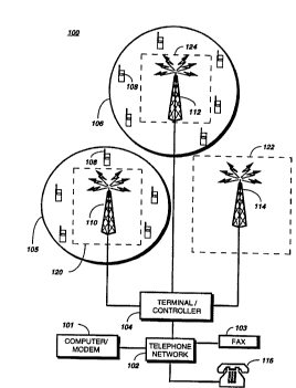
Referring to FIG. 1, a selective call comrnl~nication system 100 in
accordance with a preferred embo~limPnt of the present invention is
shown. The selective call co~nmllnicAtion system 100 comprise a
terminal/controller 104 coupled to a computer (not shown) via a modem
101 and a fA~ cimilP (FAX) machine 103 and a telephone 116 via a
collvel,tional public or private telephone network 102 known to one of
ordinary skill in the art. The telephone network 102 through the
10 terminal/controller 104 is coupled to a plurality of selective call base
stations (or sites) 120-124. The plurality of selective call base stations 120-
124 transmit and receive signals via its respective transmitters/receivers
110-114. The details of the operation of the selective call base stations 110-
114 will be rliccllcse~l below. The plurality of selective call base sites 120-124
15 have an associated coverage area (for example, 105 and 106) into which
signals from the terminAl/controller 104 are broadcast and received by at
least one of a plurality of selective call receivers 108.
RPfPrrin~ to FIG. 2, a more ~letAile~l block diagram of the selective call
base stations 120-124 are shown in accordance with the ~referl.2d
20 embo-liment of the present invention. The selective call base stations 120-
124 co~ lise a telephone inlercol,l~ect 201 which allows nle~csAges to enter
into the selective call commuPic-Ahon system 100 through a public or
private telephone network using, for example, a telephone.116, a
computer 102, a f~ccimile 103 or an alphanumeric entry device (not
25 shown). A communication terminal 202, for example the Motorola's
MODEN PLUS Encoder, processes the information received through the
telephone il.lelcorulect 201. A generated address and messAge decoded
from the received information are stored in a memory 204 until the next
traPcmicsicln cycle.
As shown, the communication terminal 202 is coupled to a controller
206, which controls the operation of a link trancmitter 208, a
communicAting transmitter 210, a link receiver 212, and a communicating
receiver 214. An example of a controller suitable for use in the present
invention is Motorola's MC6809 controller. A timing generator 216,
35 coupled to the controller 206, provides a high accuracy clock to maintain
system timing for commlmicAtion and synchronization of the selective
call communication system 100 including all the selective call base stations
WO95/06364 1~ 63 o~ PCT/US94/09312
.
120-124 and the plurality of selective call receiver 108 by techniques known
to one skilled in the arts. Operationally, the communicating tran~mittPr
210 l;ransmits, to the plurality of selective call receivers 108, a signal whichco~ ises a paging type mess~ prereldbly on a first frequency at the
tran~mi~siQn cycle. P~efe,ably, a group of selective call receivers are
intended (addressed) by the comml-nicating traI~mitter 210 to receive the
paging mess~ge. As is known, the paging mess~ge before tran~mi~sion
transmitting is encoded with the appropriate address for addressing the
group of selective call receiv~l~ of the plurality of selective call receiv~
108. Por example, and according to the preferred embodiment of the
present invention, when a group of the plurality of the selective call
rec~iv~l~ 108 have been pager, the selective call receivers of the group that
received the mess~ge will substantially simultaneously the transmit a
response, the acknowledge back signals. P,erelably, the acknowledge back
response (acknowle-lgmPnt) is tran~mitte-l on a second frequency
prt:reldbly subst~nti~lly lower than the first frequency. The receiver 214 of
the selective call base stations 120-124 receives the acknowledge back
respol se (acknowle-lgment signal or ack-back signal) which is stored in a
mPmory 204. As is well known, the receiver 214 demodulates the ack-back
signal to produce ~rereLably a b~h~nd signal. The baseband signal is
cc,llvtlled (~igiti7e~1) from an analog signal to a digital signal by an analog-to-digital (A/D) converter 220 known to one of ordinary skill in the art.
The coll-v~l~ion by the A/D co,lvt:lLel 220 are received and stored by a
digital Signal Processor (DSP) 218. The DSP 218, for example, can incl~ e a
Motorola's DSP56100 or a Texas Instrument's TMS3000 series digital signal
proc:essors. According to the ~rerelled embo~iimpnt of the present
invention, the DSP 218 stores the rligiti7e~l samples as iigiti7e-1 bits and
continuously receives and stores the ~igiti7e~ samples until all bits of the
ack-back signal have been received and stored. The rligiti7erl samples are
retrieved and each bit is coll-velled into its spectral domain repres~nt~t;on
Plereldbly, the DSP 218 performs a Fast Fourier Transform (FFT) on each
- digitized bit to generate the frequency domain signal which comprises the
plurality of ack-back sign~l~ received as a composite time ~lom~in signal
from the responding selective call receivels of the group of selective call
receiver 108. The timing generator 216 is coupled to the DSP 218 to
provide synchronization and timing for processing the plurality of
WO 95/06364 ~ PCT/US9~/09312~
2i6~304
~ligiti~e~l bits comprising the plurality of ack-back signal. The operation of
the DSP 218 will be discussed in detail below.
Referring to FIG. 3, an electrical block diagram of a selective call
receiver is shown in accordance with the preferred embollimPnt of the
present invention. The selective call receiver 108 comprises an antenna
302 for inlelc~ling tr~n.emitte~ radio frequency (l~P) signals which are
coupled to the input of a receiver 304. The RF eign~le are preferably
selective call (paging) mP~ee~ge signals which provide, for example, a
receiver address and an ~eeori~te~ mPes~e, such as nllm~ric or
alphanllmPric mess~ge. However, it will be appreri~te~l that other well
known paging sign~ling formats, such as tone only signaling or tone and
voice signaling, would be suitable for use as well. The receiver 304
processes the RF signal and produces at the output a data stream
reprPePnt~tive of a demodulated data information. The demodulated data
inform~tion is coupled into the input of a ~eco~ r/controller 306 which
~rocesses the inforrnation in a manner well known in the art. A
tranemit~Pr 334 is coupled to ~e antenna 302 and the decoder/controller
306. A power switch 310, coupled to the decoder/controller 306, is used to
control the supply of power to the receiver 304, thereby providing a battery
saving function, and to the tr~nemitter 334 for tr~nemitting the ack-back
response subsequent to the re~ei~t of a paging mPe~e~ge which will be
further ~liec1le~ee~ in detail below.
For purposes of this illustration, it will be assumed that the POCSAG
signaling format is 1ltili7e~ which is well known in the art, although other
signaling formats could be lltili7ed as well. When the address is received
by the decoder/controller 306, the received address is compared with one
or more addresses stored in a code plug (or code memory) 322, and when a
match is ~l~tectell~ an alert signal is generated to alert a user that a selectiv
call m~cs~ge, or page, has been received. The alert signal is directed to an
audible alerting device 314 for generating an audible alert or to a tactile
alerting device 316 for generating a silent vibrating alert. Switches 320
allow the user of the selective call receiver to, :~mQI-g other things, select
between the audible alert 314 and the tactile alert 316 in a manner well
known in the art.
The message information which is subsequently received is stored in
memory 404 (FIG. 4) and can be ~cc~ocse~l by the user for display using one
or more of the switches 320 which provide such additional functions as
~W0 95~'0~361 ~ ~ ~ o ~ PCTtUS94tO9312
reset, read, and delete, etc.. SperifirAlly~ by the use of appropriate functionsprovided by the switches 320, the stored message is recovered from
memory and processed by the decoder/controller 206 for displaying by a
display 308 which enables the user to view the mPqsAge. The receipt of the
5 meSSAge by the selective call receiver 108 can automatically generate the
ack-back response to the selective call base station to inform it that the
mPssAge was s~lcce.qsfully received. Plef~dbly, the user will have the
opportunity to input a mPqs~ge by using switches 320 or some other input
devices well known to one of ordinary skilled in the arts. When the
10 mPqsAge is entered, the decoder/controller 306 processes the me~qsAge by
enco~ling an addressed derived from the received mpssAge to generate the
ack-back response. The encoded ack-back response is then tra~qmitte~ to
the selective call base station that originated the paging message by
techniques well known to one of ordinary skill in the art.
The controller/decoder 306 of FIG. 3 can be impl~men~ed utilizing a
microcoll-~ulel as shown in FIG. 4. FIG. 4 is an el~pctricAl block diagram of
a microcomputer based decoder/controller suitable for use in the selective
call receiver of FIG. 3. As shown, the microcomputer 306 is pl.2reldbly of
the MC68HC05 series microcomputers, such as mAnllfActllred by Motorola,
20 Inc., which inrl~ e~ an on-board display driver 414. The microcomputer
306 inrlllrlPs an osrill~tor 418 which generates the tiIning signals utilized
in the operation of the microcomputer 306. A crystal, or crystal oscillator
(not shown) is coupled to the inputs of the osrillAtor 418 to provide a
reference signal for establishing the microcomputer timing. A
25 timer/counter 402 couples to the osrillAtor 418 and provides
progrAmmAhle timing functions which are lltili7e-1 in controlling the
operation of the receiver or the processor. A RAM (random access
memory) 404 is llhli7P-l to store variables derived during processing, as
well as to provide storage of mP~A~e information which are received
30 during operation as a selective call receiver. A ROM (read. only memory)
406 stores the subroutines which control the operation of the receiver or
the processor which will be rli~cllssed further. It will be appreciated that in
many microcomputer implementations, the progr~mmAhle-ROM (PROM)
memory area can be provided either by a programmable read only
35 memory (PROM) or an EEPROM (Pl.och ;cAlly erasable progrAmmAhle read
only mPmory). The oscillator 418, timer/counter 402, RAM 404, and ROM
406 are coupled through an address/data/control bus 408 to a central
W095/06364 PCTrUSs4/Os312
~ '3 ~ l 8
processing unit (CPU) 410 which performs the instructions and controls
the operations of the microcomputer 306.
The demodulated data generated by the receiver is coupled into the
microcomputer 306 through an input/output (I/O) port 412. The
demodulated data is procP~se-l by the CPU 410, and when the received v
address is the same as stored within the code-plug memory which couples
into the microcomputer through, for example an I/O port 413, the
mP~ s~ge, if any, is received and stored in RAM 404. Recovery of the stored
mP~s~ge~ and selection of the pre(letPrmined destin~tion address, is
10 provided by the switches which are coupled to the I/O port 412. The
microcomputer 306 then recovers the stored me~s~ge and directs the
information over the data bus 408 to the display driver 414 which
processes the information and formats the inform~h-n for pL- s~llation by
a display 308 (PIG. 3) such as an LCD (liquid crystal display). At the time a
15 selective call receiver's address is received, the alert signal is generated
which can be routed through the data bus 408 to an alert generator 416 that
generates the alert enable signal which is coupled to the audible alert
device that was riesrrihed above. Alternatively, when the vibrator alert is
selecte-l, as described above, the microcomputer gel,e,dles an alert enable
20 signal which is coupled through data bus 408 to the I/O port 413 to enable
gneration of a vibratory, or silent alert. Switch inputs are received by the
I/O port 412 via the data bus 408. The switch inputs are procP~sed by the
CPU 410. Spe- if ic Ally, the CPU 410 retrieves the address of.the selective
call base station from RAM 404 and in conjunction with the timer counter
25 402 and the osrill~tor 418, the CPU 410 generates the ack-back signal which
is passed via the data bus 40 to the traI .~mi~r.
The battery saver operation is controlled by the CPU 410 with battery
saving sign~l~ which are directed over the data bus 408 to the I/O port 412
which couples to the power switch 310. Power is periodically supplied to
30 the receiver to enable decoding of the received selective call rec~iver
address signals and any mess~ge inform~tion which is directed to the
selective call receiver. Spe~ ific~lly, when the selective call receiver 108
begins decoding the paging signal, the receiver is powered by the power
switch. When the paging mess~ge is læeived and stored, the
35 microcomputer 306 sends a signal to the power switch 310 to disable power
to the receiver 304 and enable power to the tr~n~mittPr for transmitting the
ack-back signal.
WO 95/0636~1 PCT/US94/09312
?I-~63a~
Referring to FIG. 5, a timing diagram is shown illustrating an example
of a bit pattern of an acknowledge back (ack-back) signal of one of the group
of the selective call receiv~l~ in accordance with the preferred embodiment
of the present invention. As discllcsec~, the ack-back signal is at a frequency
lower than the paging signal from the selective call base station. The paging
signal is, for example, within a range from sixteen-to-thirty (1~30) Kbs
(kilo-bits-seconds) while the ack-back signal is, for example, within a range
of one hundred (100) bits-per-secon~1 The bit pattern 500 illustrates an
example of one of the ack-back signal of one of the selective call receiver, forexample one subchannel, of the group of selective call receivers that were
paged. The bit pattern shows bits 502, 506, 510, and 51~518 r~rese~ g
digital "ones" and bits 504, 508, and 512-514 representing digital "zeros".
The aLck-back response, ~rt:reldbly, cu~ lises a bit pattern having 300 bits,
the values of the bits depend an the inform~hon being conveyed. For
example, an N member group of selective call receiv~ls 108, subsequent to
the rnembers of the group responding by sending N or less.ack-back
responses, the selective call base station will receive composite bits
colll~lising the N or less ack-back responses within each bit time which will
be further ~1icctlcsed in detail below.
Referring to FIG. 6, a frequency lQm~in representation of a thirty (30)
KiloHertz (KHz) channel illustrating, for example, ten subchannels (ten
ack-back responses) r~pr~c~.lt;..g the frequency domain representation of
the acknowledge back signals in accordance with the ~rerelled embodiment
of the present il~v~nlion. As discussed above, since each bit received by the
25 selective call base station comprises a composite bit, then collv~lLil-g the
composite bit into its frequency representation generates a frequency
~lom~in signal illustrating the N, for example ten, ack-back signals in their
sub channels. The ~rerell.2d modulation scheme is binary-frequency shift
keying (FSK) with each of the ten selective call receivers 108 within the
30 group assigned to one of the ~re~lled ten subchannels 1-10. Each of the ten
selective call ~eCt~iVelti 108 of the group is assigned to a different
subfrequency corresponding to one of the ten subchannels for example.
The subchannels 1-10 have an a~prokilllate separation of 300 Hz between
tones representing "ones" 602 and tones representing "zero-" 612. Each
35 subchannel 1-10 is located on a central axis 650 which marks the center of
each subchannels 1-10 for decoding the "ones" or "zeros" tone of each of the
ten subchannels. As is well known to those skillp~l in the art, the oscillator
WO 95106364 PCT/US94/09312_
21~63~4
of the selective call receiver must by sufficiently accurate to pr~vent a signalin its subchannel ~qsi~nment to shift to either of its adjacent subchannels
assigned to other selective call receivers of the group.
Referring to FIG. 7, a flow diagram illustrating the decoding operation
5 of the DSP of the selective call base station is shown in accordance with the
prert:lled embodiment of the present invention. Operationally, the
selective call base station 120-124 (FIG. 2) receives and encodes the ~n~cs~ge
intPn~1erl for, e.g., a pre~signell group of selective call receivers, ~rereldbly a
group of ten. The encoded paging m~cs~ge is tr~ncmitte~l to the group of
10 selective call receivers, step 702. After trarl.cmiqsion, the selective call base
station 120-124 waits for the ack-back response from the group of selective
call receivers, step 704. Step 706 detectc when the ack-back signal is received
from the group of selective call receivers which arrive substantially
cimlllt~neously. As is well known, each selective call receiver may be
15 located anywhere in the coverage area of the selective call base station,
therefole, for example, each selective call receiver irrespective of its location
will delay before tr~ncmittin~ its ack-back signal to ensure that all selective
call receivel:j of the group will transmit at substantially ~e same time.
Each selective call receiver r~ t~5 it delay depending on received p~ing
20 signal, for example, the paging signal may cont~in information indicative
of the time of trancmi~sion which is used to determine the delay time for
tr~n.cmitting the ack-back signal.
When the ack-back signal is received, step 708, the A/D converter
includes a sample-and-hold circuit (S/H) which samples the bits, preferably,
25 at sixty (60) KHz rate, because the highest frequency present in the ack-backsignal is thirty (30) KHz. For each bit, there are six hundred (600) samples
because the frequency of the ack-back signal is one hundred (100) Hz and the
sampling frequency is 60 KHz. The samples are ~ligiti7e~ organized and
stored according to the r~Lese.~lative bit, step 710. Steps 708 and 710 are
30 repeated until all the bits of the ack-back signal are received, for example,the three hundred bits. The ~igiti7.e~1 samples representing each bit are
identified and retrieved from memory. The 600 samples are increased
(padded), ~re~ldbly, by four-hundred-and-twenty-four (424) "zeros"
resulting in one-thousand-and-twenty-four samples (1024) which is a power
35 of two as required by the Fast Fourier Transform (~ l ), step 712. The DSP
transforms the time repres~nt~tinn of the ack-back signal into a frequency
representation (frequency r~om~in signal) by performing the ~l on each bit
-
~ WO 95/06364 21 6 ~ 3 o ~ PCT/US94/09312
~ ~ r ,3 1
11
of the ack-back signal, step 714. The frequency samples are stored, and then
organized in a matrix format for subsequent processing, step 716.
Referring to FIG. 8, the matrix representation is illustrated with rows
corresponding to the number of bits and columns col.e~onding to the
5 number of frequency samples in accordance with the preferred embodiment
of the present i~ ion. The matrices 1-10 colle~ond to the subchannels
1-10 illustrated in FIG. 6. The rows of the matrix 1 is numbered 1-300
colle~ponding to the 300 bits of the ack-back signal. The column of the
matrix 1 ls numbered 1-51 representing the number of frequency samples of
10 each subchannel. As previously discussed, each bit comprises 1024
frequency samples (after p~ ing), and because the highest frequency
component present is 30 KHz then 514 high-order frequency samples may
be discarded without arre~ lil,g the integrity of the spectral signal
representation. Five hundred and ten (510) frequency samples remain for
15 the ten subchannels 1-10. Thererol~, each subchannel is repre~Pn~rl by
fifty-one (51) samples, and by processing each matrix, each subchannel can
be processed independently of the others because of its unique matrix
representation.
Referring again to ~:IG. 7, a window is generated for decoding the
20 inforun~tiotl of the ack-back responses on each of the plurality of frequency(subchannels), step 718. The window is positioned for locating the peak of
the frequency riom~in signal of the subchannel 1 across the 300 bits in the
subchannel 1, step 720. r~efelably, the window is wide enough to measure
eight lines of samples of the fifty-one (51) sample lines. Once the window is
25 position, ~rereLdbly across the lowest eight samples of the 300 bits, the eight
sample lines are ~crtlmtll~ted, step 722. The arctlmlll~ted eight sample
lines represents the total energy in the window. The window is then
shifted to the next position, preferably shifted one sample line higher, step
724. The energy is measured again by sllmmin~ (~cctlm~ ting) the original
30 seven sample lines plus the additional one sample line to obtain another
energy value for the new window position, step 726.
lReferring to PIG. 9, the frequency domain represent~tion of the bits of
the subchannel 1 coll~sponding to FIG. 5 is shown in accordance with the
yrerelled embo~im.ont of the ~resel,t invention. The frequency domain
35 signal of the time domain bit pattem (FIG. 5) shows how each bit appears
after the spectral lrdl s~ollnation of the subchannel 1. Bits 502, 506, 510, and516 represent "ones" as identified by line 904 ir~iic~ting the first half of the
WO 9~,/0~61 PCr/US94/09312_
2 ~ Q 4
12
window 902. Bits 504, 508, and 512-514 represent "zeros" as~ nhfie~ by
line 906 indicating the second half of the window 902. As discussed, the
ack-back signal is digital FSK modulated, where a binary "one" is z~Signe-l
as the lower frequency tone 602 (see FIG. 6) and a binary "zero" is ~Signerl
the upper frequency tone 612 (6CC FIG. 6). The window 902 is shown
positioned over all the bits of each subchannel, where bits 502-516
correspond to the first eight bits, and the window continues over the next
292 bits to enclose the 300 bits of each ack-back signal (subchannel).
In this way, the position of the window is shifted until the maximum
energy is located which corles~onds to the peak of the frequency domain
signal across all 300 bits of the subchannel 1.
Referring to FIG. 10, the frequency domain representation illustrates
the decoding of the bits in the subchannel by generating the window in
accordance with the ~rerelled embor~im~nt of the present invention. The
tone 602 collesponding to the binary "one" is shown, and the tone 612
co,lesponding to the binary "zero" is shown by the dotted l~nes. The
window 902 is ideally positioned to illustrate a tone occurring at its off-set
from the center 650 of the subchannel 1. The dotted line repres~ont~ti~)n of
the "zero" tone shows the location where the zero tone would occur if the
bit was a "zero" instead of a "one". It is understood the a "one" and a
"zero" occurs in ~ ion of the other.
Referring again to FIG. 7, after energy of the second window position is
measured, the energy values are compared with each other to determine
the position of the window collesponding to the maximum energy, step
728. Step 730 checks if all window positions are measured. If not, the DSP
process continues to step 724 for shifting to another window position.
When all window positions are measured, step 730, the process continues
to step 732 which divides the window 902 in half. The energy of the
window 902 is checked to ~ietprmine if the total energy ~cee~l~ a threshold
value, step 734. The threshold value inclic~tes when a signal is present on
the sub~ h~nnPl, therefore if the energy value is below the threshold, the
process stops for that subchannel, step 736. Otherwise, the process
continues to step 738 which compares the energy of the first half of the
window 902 with the energy in the second half of the window 902. If the
energy in the first half of the window 902 is greater than energy of the
second half of the window 902, step 740, the bit is decoded as a binary "one",
step 744. Otherwise the bit is decoded as a binary "zero, step 742.
~WO 95/OC3C 1 21 ~ 6 3 o ~ PCT/US94/09312
13
In this way, the invention decodes a plurality of subchannels
representing responses from a plurality of selective call rec~ivel~. Each
selective call receiver responds on a preassigned subchannels, and although
there are ~,erelably a maximum of ten selective call leceive,s capable of
5 responding substantially simlllt~neously, the invention does not require a
ten s~eparate bandpass filters to receive each ack-back signal on each
subchannel. A filter on each subchannel would not provide a cost effective
solution for decoding the plurality of ack-back signals. Furthermore, since
the fiilter's response could not be less that the total subchannel to ensure the10 receipt of the ack-back signal, the signal-to-noise ratio (SNR) would decrease
by at least a ratio of 51-to-8 because the window is able to detect the peak of
the ack-back signal within a resolution of eight samples while the filter's
response would at least have to be as wide as the 51 samples to ensure that
the signal is not micse-l
Even if the response of the bandpass filter of each subchannel was
reduced below the size of the subchannel to improve the SNR, the
reduction would cause the filter to fail to detect the ack-back bits that fall
outside the filter's resyo~lse but are still inside the allocated subchannel.
The,e~ore, by ~ l the composite bits and decoding the plurality of ack-back
20 signals in the frequency iom~in~ the invention eliminates the need for a
plurality of filters, thereby providing a cost effective way for detecting a
plurality of ack-back sign~lc from a plurality of selective call receivers whilema~imi7ing the SNR of the received signal.
FIG. 11 is a flow diagram illustrating the operation of the selective call
25 receiver in accordance with the ~rere,led embodiment of the present
invention. The selective call receiver 108 receives the paging signal from
the selective call base station, step 1102, and decodes its address and a
meSS~ge, if any, contained therein, step 1104. The paging signal ~lereLably
co~ ;ses a tirne of tra~mi~sion which is also ~eco~p~l~ step 1104, to enable
30 the selective call receiver 108 to calculate a delay time before it responds by
sending an the ack-back response. The address of the selective call base
- station is also decoded from the received paging signal, step 1106. The
selective call receiver 108 delays until a message is entered or until the time
to transmit the ack-back response, step 1108. rrerelably, the selective call
35 receiver 108 provides an option to enable the user to enter, by techniques
well known in the art, a mpss~e to be incorporated in the ack-back
response, step 1110. If the mess~ge is not entered or the time to transmit
WO 95/06364 . . PCTIUS94/0931~
2i~3~4
14
has not elapsed, the process continues to step 1108. Alternatively, if a
mPss~ge is entered, the mPss~ge is encoded with the address of the base
station, step 1112, or if the time has elapsed, the ack-back signal is encoded
with a default mp~s~ge. In some instance, the selective call receiver may
5 not need to receive an address from the trancmitting selective call base
station, and simply transmits its mp~s~ge on its preassigned subchannel to
the selective call base station. Upon recei~t and encoding of the ack-back
message, the selective call receiver delays until its time to transmit the ack-
back response, step 1114. The ack-back response is tr~n~mitte.l to the
10 selective call base station, step 1116.
In this way, the plurality of selective call receivel in a group, by
decoding the tran~mi~sion time of the paging signal, knows the longest
time to receive the page and transmit an ack-back mp~s~ge of any selective
call receiver in the outer edge of the coverage area. The selective call
15 receiver is the able to delay for an ay~ro~riate time indicative of its current
location ensuring that the plurality of selective call receivers respond
substantially simultaneously.
In s-1mm~ry, a selective call base station receives a signal that
.:o~ rises a plurality of communication signals. The selecthe call base
20 station comprises an Analogto-Digital (A/D) converter for ~ligiti7ing the
signal into a plurality of ~iigiti7e~ bits. The A/D CO1LVerte1 further
co~ lises a Sam~?ling-and-Hold (S/H) circuit for sampling the signal at a
predetPrmine~ sampling rate generating a plurality of ~ligiti7etl samples for
each of the plurality of ~igiti~e~l bits. A mPmory stores the signal
25 corresponding the plurality of ~igiti7e~ samples, and a Digital Signal
Processor (DSP) CO11V~1lS each of the plurality of riigiti7e~1 bits into a
frequency domain signal that coll~lises a plurality of frequency samples.
The DSP further coln~lises an itlPntifiPr identifying the plurality of
~ligiti7e-1 samples colle:j~onding to each of the plurality of ~1igih7e-1 bits. A
30 padding circuit increases the plurality of ~iigiti7er~ samples of the plurality of
digitized bits to a power of two. The DSP performs a Fast Fourier
Transform (~l) on the plurality of riigih~e~l samples collesponding to each
of the plurality of ~iigih7.eri bits to generate the plurality of frequency
samples. A table or~ni7Pr organizes the plurality of frequency samples in a
35 matrix which has a number of rows comprise the plurality of ~iigiti7e~1 bits
and a number of columns coll~l;se the plurality of frequency samples. The
memory stores the plurality of frequency samples coll~s~onding to each of
~WO 95/06364 2 1 ~ ~ 3 o ~ PCT/US94/09312
the plurality of digitized bits, and a decoder decodes the plurality of
communication signals from the plurality of frequency samples. The
decoder further comprises a generator for generating a window for
measuring energy of at least one frequency sample of the plurality of
5 ~igit;7e-1 bits in each of the plurality of cQmmllnication signals. The
generator further comprises a controller for positioning the window on a
colre~onding one of the plurality of ~igiti7e~1 bits of the frequency domain
signals. An acctlmlll~tor accumulates the at least one frequency sample in
the window for measuring the energy of the window. The controller shifts
10 the window for measuring another one of the plurality of frequency
samples. The controller continues shifting the window until the plurality
of frequency samples of the one of the plurality of comtnllnication si~n~l~
have been measured. A ~ietPrminator detPrmine.~ the at least one frequency
sample of each of the plurality of communication signals that has a
15 maximum energy. The ~let~rmin~tor further comprises a comparator for
comparing the energy of each position of the window for detPrmining the
position of the window cc,l,~onding to the maximum energy. A divider
divides the window co,le~onding to the m~x;...l~ energy into a first and
second portions, and the comparator compares the first portion with the
20 secon-l portion for determining a binary re~resentation of each of the
it; ~erl bits.
In this way, the inv~l~lion decodes a plurality of subchannels
representing responses from a plurality of selective call rec~vels. Each
selective call leceivel responds on a preassigned subch~nnel~, and although
25 there are ~lereldbly a ma~umum of ten selective call receiv~ls capable of
respo.nding substantially sin lllt~neously, the invention do~s not require a
ten separate bandpass filters to receive each ack-back signal on each
subchannel. A filter on each subchannel would not provide a cost effective
solution for decoding the plurality of ack-back si~n~l~. Furthermore, since
30 the filter's response could not be less ~an the total sub~ h~nnel to ensure
the receipt of the ack-back signal, the signal-to-noise ratio (SNR) would
decrease by at least a ratio of 51-to-8 because the window is able to detect thepeak of the ack-back signal within a resolution of eight samples while the
filter's response would at least have to be as wide as the 51 samples to
35 ensure that the signal is not mi.~se-l
WO 95/06364 ` PCT/US94/09312_
2~6~3~4 ~
16
Even if the response of the bandpass filter of each subchannel was
reduced below the size of the subchannel to improve the SNR, the
reduction would cause the filter to fail to detect the ack-back bits that fall
outside the filter's response but are still inside the allocated subchannel.
5 There~re, the invention provides a cost effective way for detecting a
plurality of ack-back sign~ from a plurality of selective call receivers while
ma~imi7.ing the SNR of the received signal.
We claim: