Note: Descriptions are shown in the official language in which they were submitted.
ACTIVE IR INTRUSION DETECTOR
- 1 -
The present invention lies in the field of infrared detectors,
i.e. detectors which monitor a room for unauthorised entry
and, to this end, analyse infrared radiation received by the
detector. There are two types of such infrared detectors,
passive and active.
With the passive infrared detectors, the detector waits until
a radiats.on source, which emits radiation that differs from
that of the environment, i.e. the temperature of which is
other than that of the environment, enters into the field of
vision. The passive infrared detectors, which are relatively
low-priced and, today, widespread, can only detect radiating
objects on the basis of this principle, and reach a limit as
soon as objects, for example valuable objects, are to be
monitored, such objects being removable with mechanical, non-
detectable means. In addition, with the passive infrared
detectors, special measures have to be taken to prevent so-
called masking, i.e. the unnoticed changing or covering of the
detector's field of vision.
In contrast to the passive detectors, the active infrared
detectors do not handle the thermal radiation given off by
objects in the field of vision, but rather actively irradiate
the room to be monitored and react to changes in the reflected
infrared radiation. In this way, they can also detect
movements of "dead", i.e. non-radiating, objects. In addition,
they can only be masked with considerable difficulty because
they detect any approach. In return, the active infrared
detectors have certain problems with sensitivity and false
alarm reliability, because the reflected infrared radiation
can be superimposed with such severe interference that
reliable detection of movements becomes impossible in
practice.
The invention concerns an active infrared detector for
detecting movements in a monitored room, having an emitter for
emitting modulated infrared radiation into the monitored room,
- 2 -
having a receiver for the infrared radiation reflected from
the monitored room and an analysis circuit, connected to the
receiver, and containing means for obtaining a working signal.
In a detector of.this type described in GB-A-2 I87 825, the
analysis circuit contains. an operational amplifier, designed
as a synchronous amplifier, which only amplifies those
incoming signals which are in phase with the emitted signal.
These signals are integrated in two integrators having various
time constants, wherein, in the non-disturbed state, both
integrators generate the same voltage, and a difference
between these voltages indicates an intruder. These infrared
detectors are not satisfactory with respect to reliability of
response because the integration of the incoming signal with
two different time constants is insufficient guarantee that
every movement of an object in the monitored room will
actually be identified. The detector is also not reliable with
respect to false alarms because the possibility cannot be
excluded that a difference between the signals from the
integrators is caused by causes other than the movement of an
object.
The invention is now intended to improve these known active
infrared detectors with respect to sensitivity, reliability
and insensitivity towards foreign influences.
The active infrared detector according to the invention for
solving the aforementioned problem is characterised in that
the analysis circuit has a controller for emitting a
compensating signal superimposed over the incoming signal, the
controller on the one hand receiving the working signal and on
the other hand being connected to the output of the receiver,
and that the compensating signal is selected so that the
working signal is corrected to the value zero.
Correction of the working signal to the value zero has the
advantage that the maximum sensitivity is retained at all
- 3 -
times; the receiver therefore works in the same way as a self-
balancing scale. The direct result thereof is that an unwanted
interference signal, provided that it is of the same frequency
and phase as the emitted infrared radiation, is also
compensated to zero and does not cause the receiver to be
restricted to minimum sensitivity. Interference signals of
other frequencies are not so critical because they can be
simply filtered out.
A first preferred embodiment of the infrared detector
according to the invention is characterised in that a common
optical system is provided for the emitter and receiver. The
use of a common optical system enables a massive reduction in
the manufacturing costs and dimensions, and enables a maximum
range to be obtained for a low power consumption.
A second preferred embodiment of the infrared detector
according to the invention is characterised in that the
analysis circuit has an analogue/digital converter, connected
downstream of the controller, the digitised signal being
obtainable at one output thereof and the other output thereof
being connected to a digital/analogue converter for generating
a voltage corresponding to the digital signal value in each
case, and characterised in that this voltage is used to
generate the compensating signal. Digitisation of the
controller signal has the advantage that it enables more
differentiated and intelligent signal analysis than used to be
the case.
Such signal analysis is possible particularly if, as in a
further preferred embodiment of the infrared detector
according to the invention, one of the outputs of the
analogue/digital converter is connected to a microprocessor.
The microprocessor enables, on the one hand, an increase ir_
the resolution and, on the other hand, creates the
prerequisite for coupling the sensor present in the infrared
detector to a second sensor working according to another
- 4 -
detection principal, and analysing the signals of both sensors
together.
The invention is explained in greater detail below with
reference to embodiments illustrated in the drawings, which
show:
Figure 1 a diagrammatic sectional representation of an
infrared detector according to the invention,
Figure 2 a block diagram of a first embodiment of the
analysis circuit of the infrared detector in
ffigure 1,
Figure 3 a detail variant of the circuit in figure 2, and
Figure 4 a block diagram of a second embodiment of the
analysis circuit of the infrared detector in
figure 1.
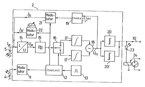
The active infrared movement detector 1 illustrated in figure
1 essentially consists of an emitter S, which
irradiates the room to be monitored with pulsed infrared
light, of a receiver E for the infrared radiation reflected
from the monitored room, of an electronic analysis and control
circuit 2 and of a power supply unit 3. According to figures 2
and 4, the emitter S is formed by an infrared light-emitting
diode (IRED) 4 and the receiver E is formed by a photodiode 5.
The emitter S, receiver E, electronic circuit 2 and power
supply unit 3 are arranged in a common housing 6, which is
mounted in the room to be monitored at a suitable point, for
example on a wall or on the ceiling.
The power supply unit 3 is connected to an external power
source and contains a fixed voltage regulator (not shown). In
the region of the emitter S and the receiver E, the housing 6
contains a window 7 which is permeable to infrared. In
- 5 -
addition, a suitable optical system 8 is provided, which
naturally must not be arranged between the window 7 on the one
hand and the emitter and receiver S and E on the other hand,
but rather can be integrated into the window 7. The optical
system 8 can be a lens or mirror optical system.
It is essential that a common optical system be provided for
the emitter S and receiver E. In other words, this means that
the receiver E "looks" into precisely those regions of the
monitored room that the emitter S is covering with infrared
radiation. This also enables, for the same power consumption,
a greatly increased range or, for the same range, a massively
reduced power consumption. A screen 9 is arranged between the
emitter S and receiver E in order to prevent a direct light
connection between these two elements. As can also be seen
from figure 1, the electronic circuit 2 has an alarm output 10
for the alarm signals obtained from the signal analysis. These
alarm signals can activate an internal alarm display
incorporated into the detector 1 and/or an external alarm
display.
According to figure 2, the infrared light-emitting diode 4 is
connected upstream of a first modulator 11, by means of which
the radiation emitted by the infrared light-emitting diode 4
is suitably modulated. Preferably, this radiation consists of
a continuous sequence of pulses and pauses between pulses so
that the room to be monitored is irradiated with pulsed
infrarecl light. It may also be sensible to insert a longer,
pre-determined emission pause between a sequence of a certain
number of pulses and pauses between pulses. In this case, the
monitored room is irradiated by pulse trains or pulse packets
which are intermittently emitted and interrupted by emission
pauses. In this way, the emission pauses can stand in a fixed
or variable time ratio to the pulse trains. The first
modulator 11 is controlled by a control stage 12, which
obtains its clock pulse from a clock pulse generator 13. In
particular, the control stage 12 determines the time sequence
~~J~~
- 6 -
and the length of the signals output to the infrared light-
emitting diode 4.
The infrared radiation emitted by the infrared light-emitting
diode 4 is bundled by the optical system 8 (figure 1) and
directed into a specific region of the monitored room. The
infrared radiation reflected from this region is collected by
the optical system 8 and routed to the light-sensitive diode
5. From the diode 5, the received infrared radiation is
converted into a proportional current (incoming signal) Ie
which is supplied to the current/voltage converter 14
connected downstream of the diode 5 and is converted by the
current/voltage converter 14 into a voltage (incoming signal)
Ue. The converter 14 also acts as a kind of filter for uniform
light by suppressing light originating from the sun and from
the room lighting. In a frequency filter 15 connected
downstream of the current/voltage converter 14, unwanted
frequencies are filtered out of the incoming signal Ue,
whereby interference caused by incandescent, fluorescent and
discharge lamps, in particular, is suppressed. The output of
the frequency filter 15 is connected to a separating filter 16
that is controlled by the control stage I2 in the clock pulse
of the infrared light-emitting diode 4 modulation.
The output signal from the frequency filter 15, which is
largely free of interference, is supplied via the separating
filter 16 alternately to one of two integrators 17, 17'. In
this way, the separating filter 16 is controlled by the
control stage 12 so that, for the emission duration of the
pulses, the incoming signal Ue is routed to one of the
integrators, for example to the integrator 17, and, for the
duration of the pauses between pulses, the incoming signal Ue
is routed to the other integrator, for example the integrator
17'. During any emission pauses between the pulse trains or
pulse packets, the separating filter 16 moves into a neutral
position in which neither of the two integrators 17 or 17'
_ 7 _
receives the incoming signal. The separating filter 16 is
preferably formed by a controlled switch.
Since the separating filter 16 is controlled in the modulation
clock pulse, the integrator 17 only receives the reflected
infrared emission signal, including any residues of the
filtered interference signal, from the emission pulse period,
and the integrator 17' only receives any residues of the
filtered interference signal from the period of the pauses
between pulses, with the result that the reflected infrared
emission signal can be obtained simply by calculating the
difference between the output signals from the two integrators
17, 17'. The aforementioned difference calculation takes place
in a stage 18 connected downstream of the two integrators 17,
17'. The output signal from this stage 18 is the infrared
emission signal U~, reflected from the monitored room and
largely freed of interference, which forms the working signal
for the signal analysis.
Provided that the conditions in the monitored room remain
unchanged, the reflected infrared emission signal will also
remain constant. However, if an object moves in the monitored
room, regardless of whether the object is a living being, a
machine or any other object, then there is a corresponding
change in the reflected infrared emission signal. Gaseous
materials only influence the reflected signal if the
reflection behaviour of the room or room section containing
the material concerned changes. This means that simple air
movements, such as warm air rising from a space heater, for
example, are not detected by the detector and consequently
cannot trigger a false alarm, whereas the sudden appearance of
vapours or smoke and the like does change the reflection
behaviour and is therefore detected by the detector.
The working signal Un is routed, on the one hand, to a
controller 19 and, on the other hand, to two comparators 20
and 20'. The output of the controller 19 is connected to the
_ g -
input of a second modulator 21, the second input of which is
connected to the control stage 12 and the output of which is
connected to the input of the current/voltage converter 14.
The second modulator 21 superimposes a compensating current
Ik, in phase opposition, over the signal from the photodiode
5, wherein the time conditions for the superimposition of this
compensating current are determined by the control stage 12.
The controller 19 changes the compensating current Ik until
the output signal from the stage 18, i.e. the working signal
Un, becomes zero. Thus, the maximum sensitivity is always
retained.
The control circuit can be compared to a self-balancing scale
or to a bridging circuit, wherein the zero value of the
working signal represents the at-rest position. Each infrared
signal received, even the unwanted basic signal, is
compensated to zero. Only in this way is there the option of
using a common optical system 8 for the emitter and receiver S
and E (figure 1). This is because reflections caused on the
emitter side by lenses, mirrors and/or infrared windows, which
generally exceed by a power the reflection signal of a
possible object in the monitored room, are suppressed by the
control circuit. A highly reflective object in the field of
vision of the detector does not lead to a loss of sensitivity,
but rather is compensated away, and the maximum sensitivity is
retained.
The comparators 20 and 20' are used for signal analysis. They
compare the working signal Un with an upper limit value
(comparator 20) and a lower limit value (comparator 20') and,
if the working signal exceeds upper limit value or falls below
the lower limit value, sends an alarm signal to the alarm
output 10. Despite the described working signal compensation,
this signal analysis can take place because the entire control
operation is, in fact, so slow that, even in the event of very
careful and slow intrusion into the monitored room, the
infrared signal received by the photodiode 5 is not
- 9 -
immediately corrected to zero, with the result that both
comparators 20, 20' still have sufficient time for detection.
On account of the considerable magnitude of the interference
reflections caused by an imperfect optical system 8 or window
9 (figure 1), the controller must compensate for a very large
amount, generally over 90%, of all the reflections, wherein
the interference reflections have a fixed value, determined by
the geometry and material of the optical system and window. It
would be desirable to equalise this fixed value by means of an
additional fixed compensating current Ik,, which would
considerably reduce the amount of the total reflections to be
compensated by the controller 19 and considerably increase the
resolution. In this case, the controller 19 would have to
absorb any deviations caused by production tolerances and/or
copy tolerances of the infrared light-emitting diode 4, in
addition. to the reflections from the monitored room.
As can be seen from figure 2, a third modulator 22, also
controlled by the control stage 12, is provided for generating
the compensating current Ik,. This is either set to a fixed
value for the compensating current Ik, or is, as shown in the
figure, designed to be adjustable. In the latter case, the
compensating current Ik, can be adjusted so that the deviations
caused by the infrared light-emitting diode 4 are compensated,
as well as the aforementioned interference reflections.
The behaviour of the controller 19 is approximately
logarithmic. If it requires a certain time t to correct a
small change in the working signal, then the correction of a
change of ten times the magnitude requires only twice the time
2t. This behaviour is particularly advantageous when the
detector is switched on, when the change in the working signal
is 100% and the time required for the correction is
nevertheless not unnecessarily long.
- 10 -
The alarm signal at the alarm output 10 can be further
analysed, for example tested for plausibility, which can take
place in the detector or in a control room, or it is routed
without further processing to a control room where the alarm
is then triggered. The alarm signal can additionally or
alternatively activate a light-emitting diode 23 arranged in
the detector. According to the illustration, a relay 24 is
also provided, the contacts of which enable potential-free
analysis of the alarm signal. By separately testing the output
signals from the two comparators 20 and 20' for their sign,
i.e. by analysing the positive or negative changes in the
reflections, the direction of movement of an object in the
monitored room can be determined, either at the detector or
away from the detector.
Figure 3 illustrates a further option for suppressing or
compensating for unwanted reflections. In this variant, in
which a third modulator 22 (figure 2) is not required, the
photodiode 5 forming the actual movement detector is connected
in parallel to a second photodiode 5', preferably having
identical data with reversed polarity. In this way, the
geometry of the arrangement is selected so that one of the
photodiodes 5 is arranged in the focal point of the optical
system 8 (figure 1) and the second photodiode 5' is arranged
outside the focal point. In this way, one of the photodiodes 5
receives the reflected radiation from the monitored room plus
any interference reflections, whereas the second photodiode 5'
receives only the interference reflections. Thus, the
difference between the photoelectric currents of the two
photodiodes 5 and 5' corresponds to the desired signal from
the monitored room, which can, if necessary, be superimposed
by interference signals, such as solar radiation or room
lighting.
If two identical photodiodes 5, 5' are used, the temperature
coefficients of the photosensitivity are mutually compensated
with respect to the common incoming signal. In addition, all
- 11 -
those influences and potential sources of interference which
act on both photodiodes remain without effect. Influences or
interference of this type are, in particular, copy deviations
and temperature drifts of the infrared light-emitting diode 4
and copy deviations and changes over time in the reflection
constants of the relevant mechanical components, such as
varying dyes and surface structures. Thus, the controller 19
and the second modulator 21 simply have to compensate for the
infrared signals reflected from the monitored room, whereas
around 950 of the total reflections and photoelectric currents
are compensated by the second photodiode 5'. In this way, the
influence of the controller 19 can be reduced to around ~ 50,
which increases the resolution of the working signal Un by a
multiple of approximately ten, which corresponds to around ten
times the response sensitivity for constant comparator 20, 20'
limits.
The aforementioned checking of the alarm signal for
plausibility, which is intended to enable false alarms to be
suppressed as completely as possible, is particularly
meaningful in the so-called dual detectors, i.e. detectors
with sensors working according to two different principles.
Such known dual passive infrared movement detectors combine
the possible infrared radiation with ultrasound or microwaves.
In the present active infrared movement detector, a
combination of active/passive infrared is feasible. Such a
combination would be preferable to the known combinations of
infrared/ultrasound and infrared/microwaves, not least because
the infrared radiation behaves in exactly the same way as the
visible light and is thus controllable with the known optical
means on the basis of the visible light. The latter
advantageous characteristic of infrared radiation is
particularly important, particularly when protecting easily
penetrated surfaces with an infrared curtain, for example when
protecting pictures or sculptures in galleries or museums, or
when protecting entire window surfaces.
~~J~
- 12 -
The analysis circuit 2' illustrated in figure 4 differs from
the analysis circuit 2 in figure 2 essentially in that another
controller is used and that the controller signal is converted
from analogue to digital and is thus available for analysis in
a digitised form. According to the illustration, in this
embodiment, the first modulator I1 is controlled by a program
control stage 26 which has, amongst other components, a
counter 27. The program control stage 26 receives its clock
pulse from a clock pulse encoder 13 and determines the
sequence over time and the length of the signals output to the
infrared light-emitting diode 4. A temperature sensor for
compensating for the response to temperature changes of the
control circuit containing the infrared light-emitting diode 4
and the photodiode 5 is designated by reference numeral 28.
The signal processing takes place in a similar manner to that
in the analysis circuit illustrated in figure 2, up to the
stage 18 connected downstream of the two integrators 17 and
17'. The output signal Un of the stage 18, which forms the
working signal for the signal analysis, is supplied to a
controller 29, which is preferably a so-called PID controller,
i.e. a controller having a proportional, an integral and a
differential part, and passes therefrom into a voltage/pulse-
width converter 30. This generates, from the analogue output
signal from the controller 29, a pulse-shaped signal, in which
the total of pulse plus pause between pulses is constant and
the width (duration? of the pulse is proportional to the
signal from the controller 29. The pulse-shaped signal from
the converter 30 enters the program control stage 26, the
counter 27 of which counts the clock pulses per width of each
of the pulses of this signal. On account of the
proportionality between the pulse-width and the output signal
from the controller 29, the number of clock pulses per pulse-
width determined by the counter 27 represents a digital image
of the analogue output signal from the PID controller 29.
- 13 -
The pulse-width obtainable at the output from the
voltage/pulse-width converter 30 will only exactly coincide in
very rare cases with a multiple of the clock pulse and can
vary therefrom by up to ~ 1d (d = smallest information unit).
The constant length of pulse + pause between pulses is
determined by the program control stage 26 and can be
approximately 1 ms for a clock frequency of 4 MHz and when
using a 12-bit counter. Thus, 1,000 results of up to 12 bits,
i.e. 4,096 information units, with a precision of ~ 1d plus
any converter 30 error, are available every second.
Since the differential part of the signal supplied to the PID
controller 29 can lead to a certain instability of the digital
signal, it is advantageous to supply this signal part to a
differential controller 31. In so doing, the differential part
can be divided between the two controllers 29 and 31, or the
entire differential part can be routed to the differential
controller 31, or the differential controller can also be
omitted and only a PID controller 29 used. The essential
factor in which of these solutions is selected is, not least,
the ratio between cost, on the one hand, and sensitivity and
reliability, on the other hand. It should be stressed,
however, that all three solutions are fully functional and
provide satisfactory results.
The values of the clock pulses determined by the counter 27
pass from the program control stage 26 into a pulse-
width/voltage converter 32, in which a voltage corresponding
to the counter value is formed, with reference to a reference
voltage related to the reference voltage source 25, this
voltage determining the compensating current Ik. Here, a
precision of ~ 0.001 ~ is achievable without further means,
with the result that the compensating current precisely
corresponds to the level of the counter 27. The output of the
differential controller 31 is also connected to the pulse-
width/valtage converter 32 and routes thereto the higher-
frequency parts of the working signal Un. The output of the
- 14 -
converter 32 is connected to one of the inputs of the second
modulator 21 (figure 2), the second input of which is
connected to the program control stage 26 and the output of
which is connected to the input of the current/voltage
converter 14.
The second modulator 21 superimposes the compensating current
Ik, in phase opposition, over the signal from the photodiode
5, wherein the time conditions for this superimposition are
determined by the program control stage 26. The PID controller
29 changes its output signal and thus the pulse/pause ratio
such that the output signal from the stage 18, i.e. the
working signal Un, become equal to zero. Thus, the level of
the counter 27 corresponds to the infrared image of the
monitored room, up to the aforementioned possible deviation of
+ 1d.
Although, in practice, this deviation is of no significance,
the precision can be further increased by calculating the mean
of a plurality of individual values. Such a mean calculation
can, for example, be carried out by the counter 27 or by a
microprocessor 33 connected downstream of the program control
stage 26. With this, the infrared signal, which is present in
the program control stage 26 in a digital form, can be
analysed in a more differentiated and intelligent manner,
which leads to higher resolution and thus to improved
detectian reliability and to improved reliability with respect
to false messages. In addition, the microprocessor facilitates
a meaningful coupling of the described measurement principle
with a second measurement principal in a so-called dual
detector. The microprocessor 33, which passes the alarm
signal, which is present in the form of the result of the
analysis, to the alarm output 10, can check the alarm signal
for plausibility and thus relieve the burden on the control
room.
- 15 -
The described electronic analysis circuit with its control
circuit, which is comparable to a bridging circuit in which
the zero value of the working signal represents the at-rest
position, offers a range of advantages:
- The electronic compensating circuit suppresses the
influence of highly reflective objects close to the detector
to such an extent that the background radiation is still
identifiable. Highly reflective objects are compensated away
and the maximum sensitivity is retained.
- The electronic compensating circuit enables the use of a
common emission/reception optical system. This is because
reflections from lenses, mirrors and/or from the infrared
window, caused on the emission side, which exceed by a power
the reflection signal of a possible object in the monitored
room, are suppressed by the control circuit.
- The digitisation of the signal offers the option~of
detecting absolute infrared radiation values and thus allowing
true presence detection, and enables the use of a
microprocessor with all the associated advantages.
- The detection of the absolute infrared radiation value
enables the sign thereof to be identified, i.e. identification
of whether a positive or negative change in the reflection and
thus the movement of an object takes place close to or away
from the detector.
- The recommended analogue/digital converter is
substantially less expensive than any commercially available
A/D converter of the same resolution.