Note: Descriptions are shown in the official language in which they were submitted.
2~ ~s~~G
-1_
IMPROVED FIELD EMISSION DEVICES HAVING CORRUGATED
SUPPORT PILLARS WITH DISCONTINUOUS CONDUCTIVE COATING
Field of the Invention
This invention relates to methods for making improved field emission
devices and, in particular, to methods for making field emission devices, such
as flat
panel displays, having corrugated and locally conductive support pillars for
breakdown resistance.
Background of the Invention
Field emission of electrons into vacuum from suitable cathode materials
is useful for a variety of field emission devices including flat panel
displays. Support
pillars are important components of field emission devices (FEDs). A typical
field
emission device comprises a cathode including a plurality of field emitter
tips and an
anode spaced from the cathode. A voltage applied between the anode and cathode
induces emission of electrons towards the anode. In flat panel displays an
additional
electrode called a gate is typically disposed between the anode and cathode to
selectively activate desired pixels. The space between the cathode and anode
is
evacuated, and integrated cylindrical support pillars keep the cathode and
anode
separated. Without support pillars, the atmospheric pressure outside would
force the
anode and cathode surfaces together. Pillars are typically 100-1000 ~.m high
and
each provides support for an area of 1-10,000 pixels.
While cylindrical pillars may provide adequate mechanical support, they
are not well suited for new field emission devices employing higher voltages.
Applicants have determined that increasing the operating voltage between the
emitting cathode and the anode can substantially increase the efficiency and
operating life of a field emission device. For example, in a flat panel
display,
changing the operating voltage from 500 V to 5000 V could increase the
operating
life of a typical phosphor by a factor of 100. However, insulator breakdown
and
arcing along the surface of cylindrical pillars precludes the use of such high
voltages.
If a cylindrical insulator is disposed between two electrodes and
subjected to a continuous voltage gradient, then emitted electrons colliding
with the
dielectric can stimulate the emission of secondary electrons. These secondary
electrons in turn accelerate toward the positive electrode. This secondary
emission
can lead to a runaway process where the insulator becomes positively charged
and an
arc forms along the surface. Accordingly, there is a need for a new pillar
design that
will permit the use of higher voltages without arcing.
CA 02166506 1999-08-11
-2-
It is known to produce a corrugated dielectric pillar structure and a
multilayer pillar.
These structures increase the surface length of the dielectric material and
reduce the
detrimental effect of secondary electron emission from the pillar surface. The
present
application discloses a further improved pillar structure using discontinuous
conductor
coating with resultant improvement in resistance to breakdown and arcing of
the pillars in
high voltage environment.
Summary of the Invention
In accordance with one aspect of the present invention there is provided in an
electron
field emission device comprising an emitter cathode, an anode and a plurality
of insulating
pillars separating said cathode and anode, the improvement wherein: at least
one said pillar
comprises a corrugated rod of insulating material, said corrugations
comprising ridges and
recessed regions, and said ridges of said corrugations selectively coated with
conductive
material.
In accordance with another aspect of the present invention there is provided a
method
for making an electron field emission device comprising an emitter cathode
electrode, an
anode electrode and a plurality of insulating pillars separating said
electrodes, comprising the
steps of providing said electrodes; forming a corrugated rod of insulating
material said
corrugations having ridges; selectively applying conductive material to the
ridges of said
corrugations; adhering said rods to one of said electrodes; cutting said rods
and finishing said
device.
Brief Description of the Drawings
FIG. 1 is a schematic block diagram of the step in making an improved pillar
structure
for field emission device according to the invention;
FIG. 2 illustrates a first method for making conductor-coating on corrugated
rods as
used in the process of FIG. l;
FIG. 3 illustrates a second method for making conductor-coating on corrugated
rods
as used in the process of FIG. 1;
FIG. 4 illustrates a third method for making conductor-coating on corrugated
rods as
used in the process of FIG. l;
FIG. 5 is a schematic block diagram of the steps for preparing the conductor-
coated,
corrugated pillar structure from uncorrugated dielectric rods;
FIG. 6 illustrates a method used in the process of FIG. 5;
FIG. 7 illustrates an exemplary method of placing the pillars on a FED device;
and
CA 02166506 1999-08-11
-3-
FIG. 8 schematically illustrates an exemplary FED device comprising the
conductor-
coated corrugated pillars.
Detailed Description
There are five considerations in optimal pillar design. First, the optimal
pillar design
is one where surface paths from negative to positive electrodes are as long as
possible for a
given pillar height. Second, it is desirable to construct the pillar so that
most secondary
electrons will re-impact the pillar surface close to the point of their
generation, rather than
being accelerated a substantial distance toward the positive electrode. This
goal is
~ advantageous because most materials generate less than one secondary
electron for each
incident electron if the incident energy is less than SOOV (or more
preferably, less than
200V). Under these conditions, secondary electrons will generally not have
enough energy to
make an increasing number of secondaries of their own. For the purposes of
this goal, "close"
is defined as a point where the electrostatic potential is less than SOOV more
positive than the
point at which the electron is generated, and preferably less than 200V more
positive. Third,
it is desirable to construct the pillar out of materials that have secondary
electron emission
coefficients of less than two, under the normal operating conditions. Fourth,
it is desirable to
have as much of the surface of the pillar oriented so that the local electric
field is nearly
normal to the insulator surface, preferably with the field lines emerging from
the surface, so
that secondary electrons will be pulled back toward the surface and re-impact
with energies
less than the abovementioned 200-SOOV. Fifth, the pillar must not be so much
wider at the
anode end so that it substantially reduces the area that can be allocated to
the phosphor
screen.
Where the field emission device is a flat panel display, the pillar material
should not
only be mechanically strong but also should be an electrical insulator with a
high breakdown
voltage in order to withstand the high electrical field applied to operate the
phosphor of the
display. For established phosphorous such as ZnS:Cu, Al, the breakdown voltage
should be
greater than about 2000V and preferably greater than 4000V.
Referring to the drawings, FIG. 1 is a block diagram of steps in making an
improved
pillar structure for field emission devices. The first step (block A) is to
provide a wire, rod, or
plate of corrugated dielectric material. The prior art describes various
methods for making
such corrugated geometry from dielectric materials such as glass, quartz,
ceramic materials
(oxides, nitrides), polymers and composite materials.
~~ss~a~
-4-
The second step (block B in FIG. 1) is to deposit on the ridges of the
corrugations a discontinuous film of conductor or semiconductor material with
low
secondary electron emission co-efficient, 8maz~ The coefficient is defined as
the ratio
of the number of outgoing electrons/number of incoming electrons on a given
surface of the material. Insulators typically have high 8m~ of 2-20, e.g., 2.9
for glass
and - 20 for MgO. Conductors or semiconductors typically have low 8m~ of less
than - 2. For FED pillar applications, a 8m~ value close to 1 is desirable.
8m~
much higher than 1 means undesirable electron multiplication. Among suitable
materials for use as a discontinuous coating, according to the invention, on
the pillar
are metals and semiconductors such as Cu (8m~ =1.3), Co (1.2), Ni (1.3), Ti
(0.9),
Au ( 1.4), Si ( 1.1 ), and compounds such as Cu 2 O ( 1. 2 ) , Ag 2 O ( 1. 0
).
The combination of discontinuous conductor coating on the protruding
ridges of the corrugated dielectric pillar with the presence of recessed
grooves is
particularly useful in improving the resistance to high voltage breakdown,
because it
provides increased surface length, secondary electron trapping inside the
grooves,
and minimum electron multiplication on the exposed, protruding surface portion
(ridges or peaks) of the corrugated pillar.
FIGs. 2A and 2B schematically illustrates a first method of selectively
adding to a corrugated dielectric body 20 a film of low 8m~ material 21 by
inclined
angle deposition (e.g. using evaporation, sputtering, spray coating
technique).
Because of the line-of sight deposition of the film material, the deposition
is
naturally limited to the ridge or peak portion of the corrugated rod or plate.
The
deposition can be carried out in a continuous manner if a long wire or plate-
shape
corrugated material is slowly moved away during deposition. A rotation of the
rod
can be utilized to ensure uniform deposition on all sides of the wire surface
(FIG. 2A).
A low 8m~ metal or compound can be directly deposited. Alternatively,
a precursor material containing the desired 8m~ material may be deposited
first and
decomposed or pyrolized during the later stage of processing. For example, Ni0
or
Ni(OH)2 may be deposited for Ni coating, and Cu0 (evaporated) or CuS04 (spray
coated as an aqueous solution, optionally with a binder material added for
enhanced
adhesion, e.g., polyvinyl alcohol) may be deposited for Cu or Cu 2 O coating.
A second method of depositing the discontinuous film of low 8m~
material is schematically illustrated in FIG. 3. A wire 30 of corrugated
dielectric
material is continuously wiped off with a wet cloth 31 or sponge-like material
lightly
wetted with a suspension or slurry containing fine particles (below - 20 p.m
size,
CA 02166506 1999-08-11
-5-
preferably below 2 ~,m size) of low 8m~ material (e.g., Cu, Co, Cu2, Ag20) or
a precursor
liquid (e.g., CuS04 or NiCl2 solution). The ridges or protruding portion of
the dielectric wire
is stained with a coating 32 the fine particles, slurry or precursor which is
later decomposed,
sintered or melted by heat treatment to leave only the desired low 8",~
material.
Alternatively, the staining can be made with a catalyst material for ease of
subsequent
electroless or electrolytic deposition. For example, the wiping cloth in FIG.
3 can be wetted
with a palladium-containing solution for staining of the protruding wire
surface. Palladium is
a known catalyst which promotes adherence of metal to a substrate during
electrochemical
deposition. After optimal intermediate baking process for decomposition of the
solution,
electroless or electrolytic plating (e.g., with Cu, Sn) is carried out for
selective metal
deposition on catalyst strained, protruding portion of the grooved dielectric
pillar wire.
A third method of discontinuously depositing low 8m~ coating is schematically
illustrated in FIG. One of the methods for shaping the corrugated structure is
the use of inert
metal mask (such as Au film) to etch out grooves in glass or quartz fiber
using hydrofluoric
acid. The Au mask used in the etching process can be left on., which is then
used as a basis
for electroplating of a lower S~,ax material (e.g., Co) if desired. The
masked, grooved
dielectric wire 41 is placed in a bath of electrolyte 44 between a cathode 43
and an anode 45.
During the electroplating process of FIG. 4, the Au mask 40 on the dielectric
wire 41 is kept
in contact with the plating electrode (cathode) 43 by gentle pressing with non-
rigid material
such as fine metal gauge or conductive elastomer. The wire is advantageously
rotated slowly
for uniform coating.
The desired thickness of the discontinuous coating of low 8,~~ material
applied by the
process of FIG. 1 is typically in the range of 0.005-50 ~m and preferably in
the range of 0.1-
2.0 Vim. Microscopically rough film may be preferred as microscopic
geometrical trapping in
the coating itself reduces the number of secondary electrons from the coating
surface.
The next step in FIG. 1 (block C) is to heat treat the deposited film to
improve the
adhesion or melt, densify the low 8m~ material or to decompose the precursor
material
coating. Typically a hydrogen-containing atmosphere is used for the heat
treatment to obtain
pure metal or alloy films, oxygen-containing, or nitrogen-containing
atmosphere can be used
for heat treatment of oxide, nitride or
- 216~~p~
-6-
other compound films. The heat treating temperature and time varies depending
on
the nature of metals or precursors, but they are typically in the range of 100-
900°C
for 0.1-100 hrs.
The final step in FIG. 1 (block D) is to cut the wire into desired pillar
length and assemble into field emission display device between the cathode and
anode.
Instead of processing on a corrugated wire as described above, a non-
corrugated wire can be used as a starting material for processing as
illustrated in
FIG. 5. The first step shown in block A of FIG. 5 is to provide a non-
corrugated
dielectric rod or wire such as illustrated in FIG. 6A as rod 60.
The next step shown in FIG. 5, block B is to deposit a continuous layer
of low secondary emission conductor or precursor. In FIG. 6B, this layer is
denoted
by reference numeral 61.
The third step (FIG. 5, block C) is to mask portions of the coated rod
with a metal mask material shown in FIG. 6C as masking elements 63.
The next step in block D of FIG. 5 is to form grooves by preferentially
etching the dielectric material. The resulting structure is shown in FIG. 6D
with
grooves 64.
The metal mask material that resists etching in hydrofluoric acid
processing for groove etch-out is chosen in such a way that the metal also has
low
8m~ characteristics. In such a case, the mask material can be simply kept and
used
as a low 8m~ coating on the exposed ridges, without having to add additional
low
8m~ metal, thus reducing the processing cost. Such a low 8m~ material that
resists
etching by hydrofluoric acid can be Au itself (Sm~ =1.4) but an even lower 8m~
mask can be accomplished by alloying of Au, or Pt (Sm~ =1. 8) e.g., with a
lower
Sm~ metal such as Co, Cu, Al, etc. The desired alloy composition is 40-80
atomic
percent Au, with the remainder made up of the selected alloying elements.
Binary or
ternary or higher order alloys can be used. The desired alloy is exemplarily
first
deposited on a round wire of dielectric material as a continuous film (e.g.,
by
physical, chemical, electrochemical means or other known techniques) (FIG.
6B),
patterned (e.g., by photolithographic or mechanical means) into a zebra-shape
or
other vertically discontinuous configuration (FIG. 6C), before subjected to
hydrofluoric acid processing as illustrated in FIG. 6D. Alternatively, the
zebra-
shaped metal layer can be directly obtained by deposition through a patterned
mask.
2~.6~~0~
_7_
A typical geometry of the pillar is advantageously a modified form of a
round or rectangular rod. The diameter or thickness of the pillar is typically
50-1000
p.m, and preferably 100-300 pm. The height-to-diameter aspect ratio of the
pillar is
typically in the range of 1-10, preferably in the range of 2-5. The desired
number or
density of the pillars is dependent on various factors to be considered. For
sufficient
mechanical support of the anode plate, a larger number of pillars is
desirable,
however, in order to reduce the manufacturing cost and to minimize the loss of
display pixels for the placement of pillars, some compromise is necessary. A
typical
density of the pillar is about 0.01-2% of the total display surface area, and
preferably
0.05-0.5°l0. A FED display of about 25x25 cm2 area having approximately
500-2000 pillars, each with a cross-sectional area of 100x100 p.m2, is a good
example.
After the corrugated rods are formed and the low Sm~ coating is added,
the next step is to adhere the ends of a plurality of rods to an electrode of
the field
emitting device, preferably the emitting cathode. The placement of pillars on
the
electrode can conveniently be accomplished by using the apparatus illustrated
in
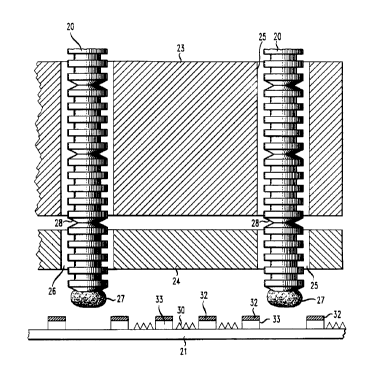
FIG. 7. Specifically, a plurality of corrugated rods 20 are applied to an
electrode 21
through apertures in a two part template comprising an upper portion 23 and a
lower
portion 24. In the insertion phase, the apertures 25 and 26 of the upper and
lower
templates are aligned with each other and with positions on the electrode
where
pillars are to be adhered. Adhesive spots 27 on the projecting ends of the
rods can be
provided to unite the rods with electrode 21. Notches 28 are advantageously
provided in the rods at desired cutting points so that appropriate length of
the rod can
be obtained. In the example shown, the electrode is the device cathode emitter
including emitter regions 30 on a conductive substrate 21. Conductive gates 32
are
separated from the substrate by an insulating layer 33.
For a FED display requiring 1600 pillars, for example, display-sized
templates (e.g., a metal sheet with drilled holes at the desired pillar
locations), are
first prepared. Through one to all of the holes (or typically one row of 40
pillar holes
at a time) are simultaneously and continuously supplied long wires of
corrugated
dielectric material. The protruding bottoms of the wires are wet with adhesive
material (such as uncured or semicured epoxy), low melting point glass, solder
that
is molten or in the paste form or an optical absorbing layer.
The corrugated rods need to be cut into support pillars. This can be
advantageously done by shearing with the apparatus of FIG. 7. The upper
template 23 is moved sideways while the lower template 24 is fixed with the
mso~o~
_g_
adhesive in contact with display cathode surface, so that the bottom pillar is
broken
away at the pre-designed V-notch location 28. This process is repeated for the
next
display substrate. Since many of the pillars are placed simultaneously, the
assembly
can be fast and of low cost. If desired, local heating may be supplied by a
focused
S light beam, e.g., a laser, to cure epoxy or to fuse the pillars to the
substrate.
The device assembly is completed by applying the other electrode and
evacuating and sealing the space between the two electrodes. Typically, the
assembly, glass sealing and evacuation process involves substantial heating of
the
device (e.g., 300-600°C). This heating step may substitute for the
heating step C in
FIG. 1. Similarly, a heating step during device assembly may be advantageous
in the
process of FIG. S. For example, the etching step (block D in FIG. 5) of an
alloy film
(e.g., Au-Cu alloy) tends to produce a surface that is depleted with Cu. The
heating
step will allow the low 8m~ component (Cu in this case) to diffuse to the
surface so
as to reduce the secondary electron emission.
The preferred use of these corrugated pillars is in the fabrication of field
emission devices such as electron emission flat panel displays. FIG. 8 is a
schematic
cross section of an exemplary flat panel display 90 using the high breakdown
voltage
pillars according to the present invention. The display comprises a cathode 91
including a plurality of emitters 92 and an anode 93 disposed in spaced
relation from
the emitters within a vacuum seal. The anode conductor 93 formed on a
transparent
insulating substrate 94 is provided with a phosphor layer 95 and mounted on
support
pillars 96. Between the cathode and the anode and closely spaced from the
emitters
is a perforated conductive gate layer 97.
The space between the anode and the emitter is sealed and evacuated,
and voltage is applied by power supply 98. The field-emitted electrons from
electron
emitters 92 are accelerated by the gate electrode 97 from multiple emitters 92
on
each pixel and move toward the anode conductive layer 93 (typically
transparent
conductor such as indium-tin-oxide) coated on the anode substrate 94. Phosphor
layer 95 is disposed between the electron emitters and the anode. As the
accelerated
electrons hit the phosphor, a display image is generated.
It is to be understood that the above-described embodiments are
illustrative of only a few of the many possible specific embodiments which can
represent applications of the principles of the invention. For example, the
high
breakdown voltage pillars of this invention can be used not only for flat-
panel
display apparatus but for other applications, such as a x-y matrix addressable
electron sources for electron lithography or for microwave power amplifier
tubes.