Note: Descriptions are shown in the official language in which they were submitted.
CA 02166507 1999-08-11
-1-
FIELD EMISSION DEVICES EMPLOYING ACTIVATED DIAMOND
PARTICLE EMITTERS AND METHODS FOR MAKING SAME
Field of the Invention
This invention pertains to field emission devices and, in particular, to field
emission devices, such as flat panel displays, using activated ultra-fine
diamond
particle material with enhanced electron emission characteristics.
Background of the Invention
Field emission of electrons into vacuum from suitable cathode materials is
currently the most promising source of electrons in vacuum devices. These
devices
include flat panel displays, klystrons, traveling wave tubes, ion guns,
electron beam
lithographic apparatus, high energy accelerators, free electron lasers,
electron
microscopes and microprobes. The most promising application is the use of
field
emitters in thin matrix-addressed flat panel displays. See, for example, the
December
1991 issue of Semiconductor International, p. 46; C. A. Spindt et at., IEEE
Transactions on Electron Devices, vol. 38, p. 2355 (1991); I. Brodie and C. A.
Spindt,
Advances in Electronics and Electron Physics, edited by P. W. Hawkes, vol. 83,
pp. 75-87 (1992); and J. A. Costellano, Handbook of Display Technology,
Academic
Press, New York, p. 254 (1992).
A typical field emission device comprises a cathode including a plurality
of field emitter tips and an anode spaced from the cathode. A voltage applied
between
the anode and cathode induces the emission of electrons towards the anode.
A conventional electron field emission flat panel display comprises a flat
vacuum cell having a matrix array of microscopic field emitters formed on a
cathode of
the cell (the back plate) and a phosphor coated anode on a transparent front
plate.
Between cathode and anode is a conductive element called a grid or gate. The
cathodes
and gates are typically skewed strips (usually perpendicular) whose regions of
overlap
define pixels for the display. A given pixel is activated by applying voltage
between the
cathode conductor strip and the gate conductor. A more positive voltage is
applied to
CA 02166507 1999-08-11
-2-
the anode in order to impart a relatively high energy (400-3,000 eV) to the
emitted
electrons. See, for example, United States Patents Nos. 4,940,916; 5,129,850;
5,138,237 and 5,283,500.
Ideally, the cathode materials useful for field emission devices should
have the following characteristics:
(i) The emission current is advantageously voltage controllable,
preferably with drive voltages in a range obtainable from off the-shelf
integrated
circuits. For typical device dimensions ( 1 pm gate-to-cathode spacing), a
cathode that
emits at fields of 25 V/~m or less is suitable for typical CMOS circuitry.
(ii) The emitting current density is advantageously in the range of 0.1-1
mA/mmz for flat panel display applications.
(iii) The emission characteristics are advantageously reproducible from
one source to another, and advantageously stable over a long period of time
(tens of
thousands of hours).
(iv) The emission fluctuation (noise) is advantageously small so as not to
limit device performance.
(v) The cathode is advantageously resistant to unwanted occurrences in
the vacuum environment, such as ion bombardment, chemical reaction with
residual
gases, temperature extremes, and arcing.
(vi) The cathode is advantageously inexpensive to manufacture, without
highly critical processes, and is adaptable to a wide variety of applications.
Previous electron emitters were typically made of metal (such as Mo) or
semiconductor (such as Si) with sharp tips in nanometer sizes. Reasonable
emission
characteristics with stability and reproducibility necessary for practical
applications
have been demonstrated. However, the control voltage required for emission
from these
materials is relatively high (around 100 V) because of their high work
functions. The
high voltage operation aggravates damaging instabilities due to ion
bombardment and
surface diffusion on the emitter tips and necessitates high power densities to
produce
the required emission current density. The fabrication of uniform sharp tips
is difficult,
tedious and expensive, especially over a large area. In addition, the
vulnerability of
CA 02166507 1999-08-11
-3-
these materials to ion bombardment, chemically active species and temperature
extremes is a serious concern.
Diamond is a desirable material for field emitters because of its negative
electron affinity and its robust mechanical and chemical properties. Field
emission
devices employing diamond field emitters are disclosed, for example, in United
States
Patents Nos. 5,129,850 and 5,138,237 and in Okano et al., Appl. Phys. Lett.,
vol. 64,
p. 2742 (1994). Flat panel displays which can employ diamond emitters are
disclosed in
the prior art.
While diamond offers substantial advantages for field emitters, there is a
need for diamond emitters capable of emission at yet lower voltages. For
example, flat
panel displays typically require current densities of at least 0.1 mA/mmz. If
such
densities can be achieved with an applied voltage below 25 V/~m for the gap
between
the emitters and the gate, then low cost CMOS driver circuitry can be used in
the
display. Unfortunately, good quality, intrinsic diamond cannot emit electrons
in a stable
fashion because of its insulating nature. To effectively take advantage of the
negative
electron affinity of diamond to achieve low voltage emission, diamonds need to
be
doped into n-type semiconductivity. But the n-type doping process has not been
reliably achieved for diamond. Although p-type semiconducting diamond is
readily
available, it is not helpful for low voltage emission because the energy
levels filled with
electrons are much below the vacuum level in p-type diamond. Typically, a
field of
more than 70 V/~m is needed for p-type semiconducting diamond to generate an
emission current density of 0.1 mA/mmz.
An alternative method to achieve low voltage field emission from
diamond is to grow or treat diamond so that the densities of defects are
increased in the
diamond structure. Such defect-rich diamond typically exhibits a full width at
half
maximum (FWHM) of 7-11 cm' for the diamond peak at 1332 cm' in Raman
spectroscopy. The electric field required to produce an electron emission
current
density of 0.1 mA/mm2 from these diamonds can reach as low as 12 V/~m.
Another approach is to coat a flat device substrate with ultra-fine diamond
particles and then to activate the particles into low- voltage electron
emitters
(<12 V/~m) by hydrogen plasma heat treatment.
CA 02166507 1999-08-11
-3a-
Summary of the Invention
A field emission device is made by pre-activating ultra-fine diamond
particles before applying them to the device substrate. This initial pre-
activation
increases manufacturing speed and reduces cost and minimizes potential damage
to the
device substrate from exposure to hydrogen plasma and high temperatures.
In accordance with one aspect of the present invention there is provided a
method for making an electron field emission device comprising a substrate
having a
conductive portion, particulate electron emitters comprising diamonds and an
electrode
adjacent said emitters but spaced apart therefrom for exciting electron
emission from
said emitters upon application of voltage, said method comprising the steps
of:
providing said particulate emitters comprising diamonds, said diamonds
predominantly
having maximum dimensions in the range of 5-10,000 nm; prior to applying said
particulate emitters to said substrate, exposing said emitters to a plasma
containing
hydrogen at a temperature in excess of 300°C while moving said
particulate emitters to
increase emitter surface exposed and to reduce agglomeration of the emitters
as
compared with stationary emitters; adhering said emitters to said substrate
conductive
portion by applying said emitters to said substrate conductive portion and
baking said
emitters on said portion at a temperature of less than 500°C in an
inert or reducing
atmosphere; and disposing said electrode adjacent said emitters but spaced
apart
therefrom.
-4-
Brief Description of the Drawings
In the drawings:
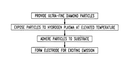
FIG. 1 is a flow diagram of a preferred process for making a field
emission device in accordance with the invention;
FIG. 2 schematically illustrates a first embodiment of apparatus useful
for practicing the process of FIG. 1;
FIG. 3 illustrates a second embodiment of apparatus for practicing the
method of FIG. 1;
FIG. 4 illustrates a third embodiment of apparatus;
FIG. 5 schematically illustrates the structure formed after the particles
are deposited on the device substrate;
FIG. b schematically illustrates the device in the late stages of
fabrication;
FIG. 7 is a top view showing a grid of emitter regions for a field
emission device; and
FIG. 8 is a schematic diagram of a field emission Bat panel display
employing the field emitters of this invention.
Detailed Description
Referring to the drawings, FIG.1 illustrates the steps for making a low
voltage field emission device. As shown in block A of FIG. 1, the first step
is to
provide diamond or diamond-containing particles. These particles preferably
have
sharp-featured geometry (polyhedral,jagged, or faceted) for field
concentration
during electron emission. The particles can be diamond grits, natural or
synthetic, or
diamond-coated (at least 2 nm thick) particles of ceramic materials such as
oxides,
nitrides or carbides (for example, Al2 O3 A1N, WC, metal particles such as Mo,
or
semiconductor particles such as Si). The melting point of the particles is
preferably
above 1000°C to avoid melting during plasma processing. The desired
range of the
particle diameters is 0.005-10 ~tm and preferably 0.01-1 ~,m. The desired
sharpness
of the particulate geometry is, in at least one location on each particle,
less than 0.5
~.m preferably less than 0.1 ~,m in radius of curvature.
The diamond content of the particles preferably consists predominantly
of ultra-fine diamond particles. Ultra-fine diamond particles are desired not
only
because of the possibility of presence of emission voltage-lowering defects
but also
because the small radius of curvature tends to concentrate the electric field.
In
addition, small dimensions reduce the path length which electrons must travel
in the
diamond and simplify construction of the emitter-gate structure. Such ultra-
fine
~~66~07
-5-
particles, typically having maximum dimensions in the range of 5 nm to 1,000
nm,
and preferably 10 nm to 300 nm, can be prepared by a number of methods. For
example, a high temperature, high pressure synthesis technique (explosive
technique) is used by E. I. Dupont to manufacture manometer diamond particles
sold
under the product name Mypolex. The ultra-fine diamond particles may also be
prepared by low pressure chemical vapor deposition, precipitation from a
supersaturated solution, or by mechanical or shock-induced pulverization of
large
diamond particles. The diamonds are desirably uniform in size, and preferably
90%
by volume have maximum dimensions between 1/3 the average and 3 times the
average.
The second step, shown in block B of FIG. l, is to activate the diamond
or diamond-coated particles by exposing them to hydrogen plasma. The particles
are
loaded into a vacuum chamber for treatment with hydrogen plasma at elevated
temperature: The plasma preferably consists predominantly of hydrogen, but it
can
also include a small amount of other elements, for example, carbon at less
than
0.5 atomic percent and preferably less than 0.1 atomic percent. The particles
are
typically exposed to the plasma at a temperature in excess of 300°C,
preferably in
excess of 400°C and even more preferably in excess of 500°C for
a period sufficient
to produce diamond-containing emitters having an electron emission current
density
of at least 0.1 mA/mm2 at a field strength below 12 V/p.m. This period
typically
exceeds 30 minutes for temperature T = 300°C, and diamond particle size
less than
1 p,m, but can be less for higher temperatures or finer particles.
The plasma is preferably generated by microwaves, but can be excited
by radio frequency (rfj or direct current (dc). Other means of creating a
source of
activated atomic hydrogen such as using hot filaments of tungsten or tantalum
heated
to above 2,000°C, rf or do plasma torch or jet, and combustion flame
can also be
utilized. In order to minimize agglomeration of the particles during the
plasma
activating processing and in order to have relative uniform activation on
major part
of the exposed diamond surface, it is desirable to have the particles in
continuous
motion so that fresh surfaces are exposed to the plasma environment and so
that the
particles do not sinter together. FIGs. 2, 3 and 4 show preferred apparatus
for
effecting such processing while the particulates are prevented from continuous
contact.
FIG. 2 is a schematic cross section of a first embodiment of apparatus
for activating the diamond containing particles in plasma environment. A
chamber 20 is advantageously constructed of microwave-transparent material
such
2166~p~
-6-
as fused quartz tube. A plurality of separately switchable microwave sources
22, 23
and 24 are disposed along the chamber, and a microwave reflector 25 is
disposed so
that sources 22, 23, and 24 produce adjacent plasma regions 26, 27 and 28
along the
chamber. Opening 28 is provided in the chamber 20 to permit entry of diamond
particles 10 and the plasma gas (mostly hydrogen) through tubes 11 and 12,
respectively. Opening 29 permits their exit. A controller 13 is provided for
selectively switching microwave sources 22, 23 and 24.
In operation, the chamber is placed within an evacuated low pressure or
atmospheric pressure container 21 and both the particulates and the plasma gas
are
flowed through. The chamber is heated to a desired temperature by radiation or
other
heating means (not shown). A plasma is ignited within the chamber by
activating
microwave sources 22, 23, 24. Movement and flow of the particulates is
achieved by
selectively switching off the plasma regions 26, 27 and 28. The fine
particulates 10
are typically electrostatically confined within the plasma regions. When
plasma
region 26 is switched off, as by switching off microwave source 22, the
particulates
in region 26 move to adjacent region 27. Similarly, when both 26 and 27 are
switched off, the particulates move to region 28. With 27 off, switching off
28
returns control of the particulates in 28 to gravity and hydrodynamic forces,
removing the particles from the plasma. Thus selective switching of the plasma
sources can move particulates through the plasma. Preferred operating
conditions are
temperature above 300° C and preferably in the range of 500-1000
°C. Gas pressure
is typically 10-100 torr, and the microwave sources are about 1 KW.
FIG. 3 is an alternative embodiment where rotation of chamber 30 and
the force of the plasma gas assists in moving the particulates. Specifically,
rotatable
quartz chamber 30 within a main chamber (not shown) is rotated by shaft 31.
The
gas is provided by one or more inlet tubes 32 preferably located at the
periphery of
chamber 30 for blowing particulates 33 toward the center of the chamber. The
overall pressure is maintained by balancing injected gas with continuous
pumping of
the main chamber through a throttle valve (not shown). Microwave source 34
provides microwave energy to establish a plasma ball 36 at the center.
Centrifugal
force extended on the particulates by rotating chamber 30 moves the particles
outwards, while the gas flow force drives them back to the center where they
are
activated. Typical operating parameters are 1 KW of microwave power, gas
pressure
of 10-100 torn, and rotation at 100-10,000 r.p.m.
.._ 2~665Q'~
FIG. 4 is a schematic cross section of an alternative apparatus for
activation of particulates 10 comprising a longitudinally extending rotatable
chamber
40 disposed within a main chamber 21. The main chamber is equipped with a
microwave source 41 and a microwave reflector 42. The rotable chamber 40 is
advantageously constructed of microwave-transparent material such as fused
quartz
and is preferably disposed between source 41 and reflector 42 so that a plasma
is
formed within chamber 40. Opening 43 is provided at the end of chamber 40 to
permit the flow of a gas (preferably H 2 ), and the chamber is attached to a
shaft 44
for rotation.
In operation, particulates 10 are loaded into chamber 40. The chamber
21 is evacuated (and optionally backfilled with hydrogen to a pressure of less
than 1
atmosphere), and the rotatable chamber 40 is rotated to tumble the
particulates 10.
The chamber 40 is heated to a desired high temperature preferably between S00-
1000°C by radiative or other heating methods. The microwave power is
then applied
to activate the particulates. Typical operating parameters are 1KW microwave
power, gas pressure of 10-100 ton, and rotation at 10-10,000 rpm.
While the exact role of the plasma treatment is not completely
understood, it is believed that the hydrogen plasma cleans the diamond
particle
surface by removing carbonaceous and oxygen or nitrogen related contaminants
and
possibly introduce hydrogen-terminated diamond surface with low or negative
electron affinity. The hydrogen plasma also removes any graphitic or amorphous
carbon phases present on the surface and along the grain boundaries. The
structure
of the nanometer diamond particles is believed to be defective containing
various
types of bulk structural defects such as vacancies, dislocations, stacking
faults, twins
and impurities such as graphitic or amorphous carbon phases When the
concentrations of these defects are high, they can form energy bands within
the
bandgap of diamond and contribute to the electron emission at low electrical
fields.
Ultra-fine materials tend to contain structural defects. For diamond, one
of the typical types of defects is graphitic or amorphous carbon phases. Other
defects include point defects such as vacancies, line defects such as
dislocations and
plans defects such as twins and stacking faults. The presence of large amounts
of
non-diamond phases such as graphitic or amorphous material is undesirable, as
they
are prone to disintegration during emitter operation and are eventually
deposited on
other parts of the display as soot or particulates. Although the exact amount
of the
graphitic or amorphous impurities in these ultra-fine diamond particles are
not
known, the low voltage emitting diamond particles in the present invention
have a
_g_
predominantly diamond structure with typically less than 10 volume percent,
preferably less than 2 volume percent and even more preferably less than 1
volume
percent of graphitic or amorphous carbon phases within 5 nm of the surface.
This
predominantly diamond composition is also consistent with the fact that
graphite or
amorphous carbon is etched away by a hydrogen plasma processing such as
described here. The pre-existing graphitic or amorphous carbon regions in the
particles would be expected to be preferentially etched away, especially at
the
surface where the electrons are emitted, resulting in a more complete diamond
crystal structure.
The diamond particles processed in accordance with the invention emit
electrons typically at fields below about 12 V/~m, more typically below about
5 V/p.m.
The next step shown in block C of FIG. 1 is to adhere a thin coating of
ultra-fine diamond or diamond-coated particles to a substrate. The part of
substrate
on which the activated emitter particles are to be adhered to can be metal,
semiconductor or conductive oxide. It can also be insulating in the event
electrically
conductive material is subsequently applied.
The preferred deposition method is direct deposition of the particles
from the plasma or CVD reactor onto the substrate. The substrate is exposed to
the
gas containing the diamond particles, and the particles are caused to contact
the
substrate either by allowing the particles to settle under gravity,
electrostatically
charging the substrate, or impinging a high-velocity gas stream containing the
diamond particles onto the substrate, and using the inertia of the particles
to separate
them from the gas. This direct deposition is one of the inventive aspects of
this
patent.
One of the alternative methods for coating the substrate is to suspend the
diamond particles in a carrier liquid and apply the mixture to the substrate.
The
diamond particles are advantageously suspended in water or other liquid, such
as
alcohol or acetone (and optionally with charged surface adherent surfactants
for
improved particle suspension) in order to avoid agglomeration of fine
particles and
for easy application on flat substrate surfaces. The suspension permits
application of
thin, uniform coatings of diamond particles in a convenient manner such as by
spray
coating, spin coating, or electrophoresis. The coating desirably has a
thickness less
than 10 ~.m, preferably less than 1 p.m, and more preferably, is only one
layer of
particles where the diamond covers 1% to 90°l0 of the surface.
2~ 66~~'~
-9-
The diamond particles activated by hydrogen plasma are inert to
ambient environment, even after exposure for months, and their low-voltage
emitting
characteristics are preserved. Thus, a mixing of pre-activated diamond
particles with
liquid and spray coating on a substrate may seem simple and trivial. However,
we
have discovered that such processing does not always result in desirable, low-
voltage
emitters unless specific processing conditions are met. One of the surprising
results
obtained is that pre-activated diamond particles (by hydrogen plasma treatment
at
900°GS hrs with measured low-voltage field emission at 1.OV/~.m) lose
their
electron-emitting characteristics completely when the liquid used is ordinary
water.
A reproducible electron emission never occurred even at a high field of - 200
V/~.m,
and the diamond exhibited breakdown when the field was raised further. Only
when
the liquid is high-purity, de-ionized water or high-purity solvent (alcohol or
acetone), the low-voltage emission characteristics of the activated diamond
particles
is retained. The exact cause for this phenomenon is not clearly understood,
but it is
speculated that certain impurity ions, if present in the liquid, modifies (or
oxidizes)
the plasma-activated surface of the diamond particles to the high work
function state
or non-emitting insulator state. Alternatively, it is possible that an
extremely thin
layer of adherent deposit, such as calcium carbonate might be deposited by the
water
and disrupt the field emission. It is therefore essential that high-purity, de-
ionized
water (e.g., resistivity > 0.1 M S2 ~ cm, and preferably > 1 M S2 ~ cm) or
high-purity
(>99.5~) solvent be used in order to effect the inventive method for
conveniently
making low-voltage emitters.
It is desirable to minimize the thermal expansion mismatch between the
diamond particles and a conductive substrate for the sake of adhesion between
the
two. Desirably, the two thermal expansion coefficients are within a factor of
10 and
preferably less than a factor of 6. For substrates whose thermal expansion
substantially differs from diamond (e.g. glass or tantalum) it is advantageous
for the
deposited film to be less than three times the thickness of a monolayer and
preferably
to be a single monolayer with 1 % to 60~ coverage. Either the emitter layer,
surface
of the conductive substrate or both, are typically patterned into a desirable
emitter
structure such as a pattern of rows or columns so that emission occurs only
from the
desired regions. The carrier liquid is then allowed to evaporate or to burn
off during
subsequent low temperature baking process. This baking treatment may
optionally
be used to promote improved adhesion of the particles onto the substrate
(e.g., by
chemical bonding such as carbide formation at the interface) or to enhance the
electron emission characteristics. A typical desired baking process is an
exposure to
2166~p~
- to -
a temperature of below -500°C for 0.1-100 hrs. in an inert or reducing
atmosphere
such as Ar, H 2 or hydrogen plasma environment.
Instead of suspension or direct deposition, we anticipate that the ultra-
fine diamond particles can also be mixed with conductive particles such as
elemental
metals or alloys like solder particles together with solvents and optionally
binders (to
be pyrolized later) to form a slurry. In this case, the substrate can be non-
conductive
and the mixture can be screen printed or dispersed onto the substrate through
a
nozzle using the known techniques to form a desired emitter pattern. The
solder
(especially the low melting temperature type such as Sn, In, Sn-In, Sn-Bi, or
Pb-Sn,
optionally containing carbide forming elements to improve solder-diamond
adhesion) can be melted to further enhance the adhesion of the diamond
particles on
to the cathode conductor and allow easy electrical conduction to the emitter
tips. As
mentioned earlier, the processing sequence or the components of materials
(liquid,
solid, or vapor) involved in the placement of activated diamond particles on
the
display surface should be carefully chosen so as not to extensively damage the
low-
voltage emission characteristics of the diamond particles.
The conductive layer on the surface of the substrate can be either
metallic or semiconducdng. It is advantageous, for the sake of improved
adhesion of
the diamond particles, to make the conductive layer with materials containing
carbide-forming elements or their combinations, e.g., Si, Mo, W, Nb, Ti, Ta,
Cr, Zr,
or Hf. Alloys of these elements with high conductivity metals such as copper
are
particularly advantageous.
The conductive layer can consist of multiple layers or steps, and one or
more of the uppermost layers of the conductive material can be discontinuous.
Optionally, for the sake of improving the uniformity of emission, portions of
the
conductive layer away from the high-conductivity diamond particle-substrate
interface can be etched away or otherwise treated to increase the impedance of
these
portions. Depending on the specific materials and processing conditions, field
emitters can be undesirably non-uniform with pixel-to-pixel variation in
display
quality. In order to substantially improve display uniformity, it is desirable
to add
electrical impedance in series with each pixel and/or each emitter, thus
limiting the
emission current from the best field emitting particles. This permits other
emitter
sites to share in the emission and provides a more uniform display. Typical
resistivity of the uppermost continuous conductive surface on which the
ultrafine
diamond emitters are adhered is desirably at least 1 m S2 ~ cm and preferably
at least
1 SZ~cm. As an upper limit, the resistivity is desirably less than lOKS2~cm.
In terms
CA 02166507 1999-08-11
- 11 -
of surface resistivity, when measured on a scale greater than the inter-
particle distance,
the conductive surface has surface resistance typically greater than 1
MS2/square and
preferably greater than 100MS2/square.
FIG. 5 shows the resulting field emitter 50 after the adhesion step
comprising a substrate 51 having a conductive surface 52 having a plurality of
activated
ultra-fine diamond emitter particles 53 attached thereto. For display
applications,
emitter material (the cold cathode) in each pixel of the display desirably
consists of
multiple emitters for the purpose, among others, of averaging out the emission
characteristics and ensuring uniformity in display quality. Because of the
ultra-fine
nature of the diamond particles, the emitter 50 provides many emitting points,
typically
more than 104 emitting tips per pixel of 100 ~m x 100 ~m size assuming 10%
area
coverage and 10% activated emitters from 100 nm sized diamond particles. The
preferred emitter density in the invention is at least 1/~m2 and more
preferably at least
5/~.m2 and even more preferably at least 20/~mz. Since efficient electron
emission at
low applied voltages is typically achieved by the presence of accelerating
gate electrode
in close proximity (typically about 1 micron distance), it is desirable to
have multiple
gate aperture over a given emitter body to maximally utilize the capability of
multiple
emitters. It is also desirable to have a fine-scale, micron-sized gate
structure with as
many gate apertures as possible for maximum emission efficiency.
The final step in making an electron field emitting device as shown in
block D of FIG. 1 is forming an electrode which can be used to excite emission
adjacent the diamond layer. Advantageously this electrode is a high density
apertured
gate structure. The combination of ultra-fine diamond emitters with a high
density gate
aperture structure is particularly desirable with submicron emitters. Such a
high density
gate aperture structure can be conveniently achieved by utilizing micron or
submicron
sized particle masks. After the activated ultra-fine diamond particle emitters
are
adhered to the conductive substrate surface, mask particles (metal, ceramic or
plastic
particles typically having maximum dimensions less than 5 ~m and preferably
less than
1 Vim) are applied to the diamond emitter surface as by spraying or
sprinkling. A
dielectric film layer such as Si02 or glass is deposited over the mask
particles as by
evaporation or sputtering. A conductive layer such as Cu or Cr is deposited on
the
dielectric. Because of the shadow effect, the emitter areas underneath each
mask
particle have no dielectric film. The mask particles are then easily brushed
or blown
away, leaving a gate electrode
- 12-
having a high density of apertures.
FIG. 6 illustrates the structure prior to the removal of masking
particles 13. The emitter layer of activated diamond particles 53 is adhered
on
conductive layer 52 on substrate 51 for providing current to the emitters.
Dielectric
layer 60 insulates emitters 53 from apertured gate electrode 61 except in
those
regions covered by mask particles 62. Removal of the mask particles completes
the
device.
In typical applications the gate electrodes and emitters are deposited in
skewed perpendicular stripes to define a grid of emitting regions. FIG. 7
illustrates
columns 90 of an emitter array and rows 91 of an apertured gate conductor
array
forming an x-y matrix of emitter regions. Emission is through apertures 92.
These
rows and columns can be prepared by low-cost screen printing of emitter
material
(e.g. in stripes of 100p,m width) and physical vapor deposition of the gate
conductor
through a strip metal mask with, for example, 100p.m wide parallel gaps.
Depending on the activation voltage of a particular column of gate and a
particular
row of emitter, a specific pixel can be selectively activated at the
intersection of
column and row to emit electrons.
The preferred use of these low voltage emitters is in the fabrication of
field emission devices such as electron emission Bat panel displays. FIG. 8 is
a
schematic cross section of an exemplary flat panel display using low voltage
particulate emitters. The display comprises a cathode 141 including a
plurality of
low voltage particulate emitters 147 and an anode 145 disposed in spaced
relation
from the emitters within a vacuum seal. The anode conductor 145 formed on a
transparent insulating substrate 146 is provided with a phosphor layer 144 and
mounted on support pillars (not shown). Between the cathode and the anode and
closely spaced from the emitters is a perforated conductive gate layer 143.
Conveniently the gate 143 is spaced from the cathode 141 by a thin insulating
layer
142.
The space between the anode and the emitter is sealed and evacuated,
and voltage is applied by power supply 148. The field-emitted electrons from
electron emitters 147 are accelerated by the gate electrode 143 from multiple
emitters 147 on each pixel and move toward the anode conductive layer 145
(typically transparent conductor such as indium-tin-oxide) coated on the anode
substrate 146. Phosphor layer 144 is disposed between the electron emitters
and the
anode. As the accelerated electrons hit the phosphor, a display image is
generated.
-13-
While specific embodiments of the present invention are shown and
described in this application, the invention is not limited to these
particular forms.
For example, the low field nanometer diamond emitters can be used not only in
flat
panel displays but also as a cold cathode in a wide variety of other field
emission
devices including x-y matrix addressable electron sources, electron guns for
electron
beam lithography, microwave power amplifiers, ion guns, microscopes,
photocopiers
and video cameras. The nanometer sizes of diamond can also be extended to
micron
sizes if suitable methods are found to impart them with sufficient
conductivity and
emissive surfaces.