Note: Descriptions are shown in the official language in which they were submitted.
2166919
APPARATIJ~ FOR MFA.~IJRTNC~T RF~T~TTVTTY OF AN FARTT-T F()RMATT()N
IJ~TN(T T~F.T TA-~ST(~MA T)T(~TTTAT ~STC~TNAT (~TFNFRATTON ANT) ~T(~TMA-T~FT TA
T~T('TTTAT T~FTF(~TT()N SYSTFM
RA~K(~TR()lJNn (lF TT-TF TNVFNTTON
L Fi~ 1 of th.o Tnvention
The present invention relates to the field of electrical resistivity tools, which are
used to measure certain properties of earth formations pe~ t~d by boreholes. More
specifically, the present invention relates to a system for digitally processing signals in
electrical resistivity tools to improve the accuracy of measurements made by the tools.
T)i~r~ inn of th~ o1ev~nt Art
F.1~tril ~1 resi~ivi~y tools are used to make measurements of electrical resi~ivily
of earth formations penetrated by boreholes. Electrical resistivity measurements can be
used for, among other things, estim~ting content of various types of fluids which can be
contained in pore spaces in the earth formations.
Electrical resistivity tools known in the art include galvanic devices. Galvanicdevices typically comprise electrodes placed on an in~ ting exterior surface of the tool.
All the electrodes on the tool typically make electrical contact with the earth formation
through a conductive fluid which fills the borehole.Some of the electrodes are connPcted
to circuits in the tool which gellel~t~ electrical current. Other electrodes are connected
to different circuits in the tool which measure voltage dirrerellces and current flow
m~gnih1de~. Measurements of voltage difference and current flow can be related to the
electrical resistivity of the earth formations.
A galvanic instrument known in the art is called a dual laterolog tool. The duallaterolog tool co~ lises electrodes which emit ~ current, and focusing electrodes
which emit focusing ~;ul-ell~s used to constrain, or focus, flow of the measuring current
in a pred~ ~l pattern. By focusing the measure current in a predetermined pattern,
216691~
mea~ulclll.;ll~ of resistivity can be related more precisely, for example, to thin vertical
section~ of the earth formation. Other pre~ r. .~ patterns for focusing the measuring
current can enable measurement of formation resis~ivily at a radial li~t~n~e closer to the
borehole, which can be useful for estim~ting movement of fluid from the borehole into
the pore space in the formation. A description of the typical electrode al~ gelllent and
current focusing paLl~llls of the dual laterolog tool can be found for example in
"Introduction to Wireline Log Analysis", by Ed L. Bigelow, Atlas Wireline Senices,
Houston, TX, 1992 (p. 59).
The tool desclil)ed in the Bigelow reference, for example, ~imlllt~n~ously makestwo dirrclcll~y focused lll~UlClllClll~ of resistivity using the same set of electrodes. The
siml11t~nPous measurements are performed by using measuring and focusing currentsystems operating at two dirrelclll frequencies. Each of the measuring and focusing
systems operates at a dirrelcnl one of the two frequencies.
In order for the dual laterolog tool to accurately record the measurements made
by each focusing and measuring system, the signals generated and detected by each
frequency system must, to the greatest extent possible, be ~lcvellled from hll~lrerillg with
each other.
Methods are known in the art for reducing hll~lrelcllce between measuring and
focusing systems opel~ g at dirrelcl~t frequencies. One method known in the art is to
provide an analog b~n-lp~s filter having a very narrow bandwidth to an input of the
voltage and current measuring circuits in the tool corresponding to each mea~urclllclll
system frequency. Analog b~n-ll)a~s filters reject passage of electrical current at
fre4u~ ies other than within a so-called frequency pa~sb~m1. One of the limitations of
analog b~ filters is tbat they can pass some current at frequencies other than within
the frequency passband. A plurality of measurement systems operating at different
frequencies may not be sufficiently isolated from each other by using analog bandpass
filters to plcvelll h~l~lr~lcllce between respective systems.
2166913
Another method known in the art for reducing inle,relc~lce between dirr~le
frequency measulclllent systems is to provide a current source for each measulclllcn
system having as nearly as possible only one frequency component. This type of source
is called a monochromatic current source. By providing a subst~nti~lly monochromatic
current source for each measurement system, detections of voltages and ~;ullcnl~ in a
particular measurement system which are not at the frequency of that particular
measurement system can be reduced.
A system for providing a subst~nti~lly monochromatic current source is known
in the art and is described, for example, in U. S. patent number 4,499,421 issued to
Sinclair. The system described in the Sinclair '421 patent comprises a pair of digital
latches and a precision resistor nclwol~ to generate a stair-step approximation of a
sinusoidal waveform. The stair-step approximation output from the resistor network is
then con-lucted to an amplifier having an analog low-pass filter. The analog low-pass
filter reduces the m~gnihlde of the "stair-steps" since they have a much higher effective
frequency than the sinusoidal signal. In addition to the limitations of analog filters as
previously descril ed herein, the system disclosed in the Sinclair '421 patent has a further
limit~tion in that the system in the Sinclair patent uses a precision resistor network to
accomplish the digital-to-analog conversion. Some of the limitations of precision resistor
l,c~wol~ used in digital-to-analog collvc,~ioll are described, for example, in U. S. patent
number 5,357,252 issued to T~7.ills, et al. The T~-17.ills '252 patent states that the
"resistive-divider" technique of data conversion, which includes the digital-to-analog
conversion of the signal generator disclosed in the Sinclair '421 patent, can be difficult
because the lc~ ive-divider technique requires using high precision analog components
which may be diffirlllt to form, particularly in a system intended to be used in the limited
space provided inside a resistivity tool used in boreholes. A resistivity tool colllp~isillg
a plurality of dirr~ ~nl measulel,lell~ and focusing systems which operate at dirrel~
frequencies, using a plurality of signal generators similar to the one disclosed in the
Sinclair '421 patent, is impractical.
2166913
It is known in the art to provide an analog-to-digital converter responsive to arange of frequencies to reduce signal distortion which can be present in analog signal
processing circuits. The Led~ius '252 patent, for example, discloses an analog-to-digital
converter responsive to a plurality of frequencies defining a usable range called the
S bandwidth. The analog-to-digital CO~ .~r in the '252 patent could be used in a multiple
frequency lc~ ivily tool if each measuring circuit for each dirr~lelll frequency could be
connected to a col-vellel similar to the co-~ve,ler disclosed in the '252 patent and
combined with a narrow bandwidth ar~alog filter. However, a limitation on the use of the
coll~ tcl of the '252 patent in a multiple frequency resistivity tool is the need to include
analog components in a filter stage of the col~vc.ler, as shown at 83 and 84 of Figure 5
in the '252 patent. The converter disclosed in the '252 patent was intended to have a
bandwidth comprising a relatively wide range of frequencies in order to be useful, for
t;A~ll~l-, in digital telephony. Tnr~ lin~ the analog components of the '252 patent in the
output stage of the Collvt;ll~l as disclosed in the '252 patent would likely allow
inte,rerellce between the dirrercl.l frequency measurement systems when used in a
multiple frequency resistivity tool.
A fur~her limh~ti-)n on using the co~vc~lel disclosed in the '252 patent is that the
disclosed co..vc,~, does not elimin~te the need for the narrow bandwidth analog b~nl1p~
filter provided at the input of the analog-to-digital converter. The limitations of using
analog b~n-lp~s filters in the measuring circuit of a multiple frequency l~si~livily tool,
as previously ~ c~1sse~1, would still apply if the co--~ .~r in the '252 patent were used
in a resistivity tool.
It is an object of the present invention to provide a resislivily measuring toolhaving a plurality of fully digital measurement circuits, each circuit capable of o~ela~ g
at a dirrelclll predetermined frequency, in order to provide mi~ h~le~relcllce
between individual measurement systems.
2166!119
It is a further object of the present invention to provide a resistivity mP~llring
tool having a plurality of monochromatic current sources each of which is fully digitally
synthesized in order to ",illi",i,P generation of spurious frequencies in the individual
llled~iUl'C ~;UllCllk;.
~;:IJMMARY OF TT-TF, TNVF,NTTON
The present invention is a tool for measuring the resistivity of an earth formation
comprising at least one measuring current source. The at least one source includes a
sigma-delta modulator and a serial bit source corresponding to a digital representation of
a predeterminPd measure current waveform. The present invention also comprises at
least one measure current sensor coupled to a delta-sigma modulator and a digital filter
which ge~ dl~s a digital output corresponding to an amplitude of said measure current
at said at least one sensor.
In a plcrcllcd embodiment of the invention the tool comprises a measure current
circuit in which a first measure current source gelleldlcs a monochromatic sinusoidal
signal having a first frequency and also comprises a first focusing current circuit which
Opeldlt~S at the first frequency. The tool of the prcr~llcd embodiment further comprises
second and third measure current sources which gelleldle monochromatic sinusoidal
signals having second and third frcq lenriPs and second and third focusing current sources
Opeld~ , at the second and third frequencies. The plcrcllcd embodiment of the invention
includes measure current sensors responsive to each measure current frequency.
RRTF.F nF,.~(~RTPTT()N OF TT-TF, T~RAWTNC'T.S
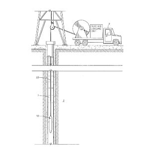
Figure 1 shows the tool according to the present invention deployed in a borehole.
Figure 2 shows a resistivity measuring tool according to the present invention.
Figure 3 shows a system for adjusting the amount of focusing current.
Figure 4 shows a measuring signal gellelatol according to the present invention.Figure 5 shows a voltage measuring circuit according to the present invention.
2166913
Figure 6 shows an ~ltern~tive embodiment of a resistivity measuring tool.
nF~RTpTTON OF TT-TF PRF.FFRRF.T) FMT~OnTMFNT
Figure 1 shows a resistivity logging tool 10 as it is typically used in a borehole
1 pellelld~ g an earth formation 3. The tool 10 is typically connrcted to one end of a
cable 33 colll~lisillg at least one in~ ted electrical conductor (not shown). The cable
33 can be extrn l~ into the borehole 1 by means of a surface logging unit 2. The cable
33 carries electrir~l power from the surface unit 2 to the tool 10, and can lldl~lllil signals
from the tool 10 to the surface unit 2. The surface unit 2 includes equipment (not shown
se~ ly) for receiving and i,lt~ ting signals tr~n~mitt~-1 by the tool 10. The surface
unit also inrlll~les e lui~ lll (not shown SæP5~IAIe1Y) for tl~ iLI;I~g control signals to the
tool 10.
Figure 2 shows a functional diagram of the tool 10 according to the present
invention. The tool 10 comprises a sonde 12 having a plurality of electrodes 14, 16,
16A, 18, 18A, 20, 20A, 22, 22A, 23, 23A disposed on an exterior in~ tin~ surface (not
shown separately) of the sonde 12. The purposes of the individual electrodes will be
further explained. The tool 10 also comprises various circuits, shown combined on a
circuit assembly 11 disposed inside the sonde 12, which measure voltage drops ofmr~llrin~ ;ullellls passing through the earth formation 3. The purposes of the various
circuits on the assembly 11 will be explained further. The measuring ~;ullclll~ are
introduced into the formation (shown as 3 in Figure 1) ~dj~cPnt to the borehole 1 by other
circuits disposed on the assembly 11.
The circuit assembly 11 is shown in more detail in Figure 2 as a functional block
diagram including lc~l~sellLdlive connections of the various circuits disposed on the
assembly 11 to the dirrelenl electrodes, as will be further explained.
The circuit assembly 11 comprises a formation voltage measuring circuit 34
conn~octecl at one input terminal to monitor electrodes 16 and 16A through a resistive
divider 27, and at the other input terminal to a ground electrode G located at the earth' s
2166919
surface, the connection to the other input tPrmin~l being made through the conductor (not
shown) in the cable 33. The formation voltage measuring circuit 34 measures a voltage
occllrring between the electrodes 16, 16A on the sonde 12 and the ground electrode G.
The measurement of the voltage made by the formation voltage mcasu~ g circuit 34 is
provided as a digital word at terminal D34A of the formation voltage measuring circuit
34. The voltage measured by the formation voltage measuring circuit 34 is related to
e~i~livily of the ear~ formation 3 adjacent to the tool 10. The voltage measured by the
circuit 34 lepLese~ a potential dirÇerellce reslllting from a current of known
magnitlllle flowing through the formation 3 between a source electrode 14 and electrodes
20 and 20A. The current of known m~gnitllde is gelle~ d by a measure current source
24, as will be further explained. The digital word present at the terminal D34A can be
con-lucted to a central processor 51, the operation of which will be further explained.
The formation voltage measuring circuit 34, which will be explained in greater
detail, can be responsive to voltages at each of three dirÇe~nl frequencies to enable
substantially ~imlllt~nPous measul~lllenl in three dirrelelllly focused measure current
systems. In the present embo~im~nt, the frequencies of the measure current systems
typically are 32, 128 and 512 Hz.
The measure current source 24, which in the present embodiment can include
three, single-frequency monochlull~lic current sources each opel~lhlg at one of the three
previously described frequencies, is connPctPd at one output I~lllPinal to the source
electrode 14, and at the other output terminal to electrodes 20 and 20A (the ~yllullt;llical
connection to electrode 20 is not shown in Figure 2 for clarity of the illustration). The
llle~ul~ current source 24 provides the current with which the voltage drop through the
earth formation 3 is measured by the formation voltage measuring circuit 34, as
previously explained herein.
A bucking voltage measuring circuit 24A, responsive to the same three
fr~lenriPs as the frequencies of the measure current source 24, is connected through a
phase m~trllPd L~ rolllæL 25 across pairs of monitor electrodes 16, 18; and 16A, 18A.
21G~gl~
The bucking voltage Illf ~ p circuit 24A lllca~ul~s a voltage drop between the monitor
electrodes 16 and 18, and symmetrically about the source electrode 14 makes the same
lll~ultllælll b~tw~ell electrodes 16A and 18A. A digital word l~lcsen~ g the voltage
drop measured by the bucking voltage measuring circuit 24A is provided at tellllillal
D24A on the bucking circuit 24A and is conrl~cted to the central processor 51. If the
voltage drop across the monitor electrodes 16, 18 (or symmetrically 16A, 18A) is non-
zero, the pl~Jcessor 51 can be plogl~ llled to adjust the current output from the measure
source 24 by ch~n~in~ the value of a digital control word con~ cted to terminal D24 on
the source 24 from the processor 51. The means by which the processor 51 adjusts the
output of the source 24 will be further explained. By adjusting the current output from
the current source 24 to m~int~in subst~nti~lly zero voltage drop between the monitor
electrodes 16, 18 and 16A, 18A, the processor 51 substantially "~i"~ .c a predetellllhled
focusing pattern of the measuring current near the wellbore 1. Because the measure
current is ~ul~ ially m~int~in~d within the predetermined focusing pattern, the voltage
drop measuled by the formation voltage m~ ring circuit 34 can be more directly related
to resistivity of the formation 3. It is known in the art to provide a single analog circuit
which provides the same function as the combined opeMtion of the bucking measuring
circuit 24, the measure current source 24 and the measure current adjll~tm~nt feature of
the processor 51, however the present embodiment is directed to a fully digital resistivity
tool.
The m~gnit~ e of the measure current ~el~ldt~d by the measure source 24 is itself
lllea~ul~d by a current ",~ circuit 26 which is responsive to each of the same three
mea~u Clll~ frequencies as is the formation voltage mP~ ring circuit 34. The current
measuring circuit 26 comprises a voltage measuring circuit (which will be explained in
more detail), of s~bst~nti~lly the same design as the formation voltage measuring circuit
34, connected across a shunt resistor 29 interposed in the measure current path b~tw~ell
the electrode 14 and the measure current source 24. Current flowing across the shunt
resistor 29 gel~ela~es a voltage drop proportional to the current flow across the shunt
216691~
resistor 29. The voltage measured across the shunt resistor 29 therefore is proportional
to the m~gnihlde of the measure current ~ l by the llle~ulc current source 24. The
m~a~urelllent made by the second measuring circuit 26 is provided as a digital word on
tçrmin~l D26A which is con~ ctçd to the processor 51. The measurement made by the
second m~lrin~ circuit 26 which is pr~ollional to current m~gnit~lde can be combined
with the voltage drop measurement made by the formation voltage measuring circuit 34
to de~llllille the resi~LiviLy of the earth formation 3.
Three focus current sources 28, 30 and 32, each opelaling at a different one of
the three previously described measurement system frequencies, are conn~cted
syl-llll~-l- ir~lly about the source electrode 14 to focusing electrodes 20 and 20A; 22 and
22A; and 23 and 23A, these electrodes being disposed on the sonde 12 at axially spaced
apart locations from the source electrode 14. Each of the focus current sources 28, 30,
32 is connected to the electrodes in a dirrelclll configuration so as to cause focusing
current from each source to flow in a different path. Each of the three dirrelc
frequency mP~cllrin~ ~;ullcllL~ ~llc~lxlhlg to one of the focusing ~;Ull~llki can therefore
constrained to a dirr~l~lll predetermined focusing pattern in the borehole 1 and the earth
formation 3 adjacent to the borehole 1. For example, a first focusing source 28, which
u~ ates at a first frequency, is conn~cted at one output to all three focusing electrodes
20, 22, and 23, and symmetrically about the source electrode 14 to electrodes 20A, 22A
and 23A (although the symm~tric connections are not shown in Figure 2 for clarity of
illustration). The other output of the first focusing source 28 is conn~cted to the cable
33 armor. The first focusing source 28 provides focusing to the measuring current
having the greatest radial depth of col~lldillL because the focusing current from the first
source 28 is col~L~ led to flow ~ull~L~llially entirely radially uuL~al-l from the sonde 12
before dispersing in the earth formation 3 and le~ g to the cable 33 armor.
A second focusing source 30, opeldling at a second frequency, is typically
conn~cted across electrodes 20 and 22 (and symmetrically 20A and 22A, but the
symm~trical connections again are not shown for clarity) to provide focusing to the
2166919
. .
second frequency llle~ul~ current having a reduced radial depth of constraint relative to
the first frequency measuring current focused by the first focusing source 28. The
focusing pattern of the second focusing source 30 enables dispersion of the measuring
current in the formation 3 at a shallower radial ~ t~nre from the sonde 12 than does the
first focusing source 28 pattern, because the second focusing current is returned to the
electrodes 22, 22A on the sonde rather than on the cable 33 armor. I~ ...,ing the
focusing current to the electrodes 22, 22A enables dispersion of the second frequency
measure current radially closer to the sonde 12, so that a relatively shallower radial
lllea~ul~ of formation l~ livily can be made by the second than can be made by the
first measure current.
A third focusing source 32, op~ g at a third frequency, can be connected
between electrodes 22 and 23 (and symmetrically to 22A and 23A with symmetrical
connections again not shown for clarity of illustration)) to provide even shallower radial
constraint of the third frequency m~uring current than the second focusing source 30
does for the second frequency measuring current. The shallower radial constraint of the
measuring current provided by the third focusing source 32 results from the focusing
electrodes 22, 23 and æA, 23A being spaced at a greater axial ~ t~nre from the source
electrode 14 than the focusing electrodes 20, 22 (and ~yllllll~lfically, 20A, 22A) used for
e",i~ the focusing current at the second frequency. The longer axial spacing of the
electrodes 22, 23 used for the third frequency focusing current enables the third
frequency measuring current to disperse in the earth formation 3 at an even shallower
Mdial ~ t~n~e from the sonde 12 than does the second frequency m~ lring current.Output levels of the focus sources 28, 30, 32 can be controlled by digital wordsinput to tellllillals D28, D30 and D32, respectively, from the processor 51.
Focusing current nlc~ulillg circuits 30A and 32A can be conn~cte~ across shunt
resistors 31 and 35, respectively, to provide measurement of the total amount of focus
current ge~ t~d by the first source 28, and the second and third sources 30, 32,e~eclively . Focusing current llleasu~ are provided as digital words on l~ll linals
2166919
D30A and D32A, lc~e~ /ely, and are conducted to the processor 51. As will be further
c~lailled, focusing current m~ les can be adjusted in response to dirrclclll values of
formation 3 resistivity so as to control the dynamic range of signal at the input of the
formation voltage measuring circuit 34 and the current measulillg circuit 26.
Figure 3 shows a flow chart of a typical measurement sequence provided by the
tool (shown as 10 in Figure 1). The focusing cullclll~ are measured by circuits 30A and
32A, as generally shown at 38. If the cullcllL~ from the sources 28, 30, 32 are
d~ ~d to be too low or too high to m~int~in a minimum predclcllllilled signal level
at the inputs of the formation voltage measuring circuit 34 and the current mr.~llring
circuit 26 as shown at number 40, adjustments are made under control of the processor
51 to the output levels of the focus current sources 28, 30 and 32 either to increase as
shown at 42A, or to decrease as shown at 42B, the level of the focus cullclll~. The
means by which the processor 51 changes the output level of the sources 28, 30, 32 will
be further explained. Changes in the amount of required focus current can occur, for
C~ , if the fluid filling the borehole 1 is particularly conductive or resistive, or the
earth formation 3 is particularly conductive or resistive. When the focus CUllC~ are
determined to be of the correct m~gnih--le, voltage drop and current m~gnitllde of the
measure ~;UllClll~ are made, as shown generally at 44.
The current sources according to the present invention can be better understood
by lcrclling to Figure 4. The source, shown as 28 in Figure 4, can also correspond to
any of the other sources shown in Figure 2 such as the focus current sources 28, 30 and
32, or the measure current source 24.
The output m~gnihlde of the source 28 is controlled by a rcrclcllce level digital
word con~lurt~ to an input t~rmin~l 58 of a reference digital to analog collvcllcl (DAC)
54 forming part of the source 28. The input termin~l 58 of the reference DAC 54 shown
in Figure 4 corresponds to any one of the digital word input terminals D24, D28, D30
or D32 of the sources 24, 28, 30 or 32, respectively, shown in Figure 2. The input
trrmin~l 58 is conn~t~d to the corresponding terminal on the processor 51. The digital
~166919
word present at the input terminal 58 is loaded into the reference DAC 54 when a load
co~ l is applied to a command terminal 56 on the lcrclcl~ce DAC 54 by the processor
51. A load ~""",~".1 is gcneldlcd by the processor 51 when the processor 51 calculates
that the value of the digital word is to be changed. As previously explained, the value
of the digital word can be changed by the processor 51 in response to measurements
provided by the focus measuring circuits 30A, 32A, and the formation voltage 34 and
current measuring 26 circuits.
The lcfercllce DAC 54 is conn~,cted to a precision voltage lerelellce source 52.The precision voltage ler~lell~ source 52 gCllCldlC~ a subst~nti~lly constant voltage direct
current (DC). The subst~nti~lly constant voltage DC from the lèrclèllce source 52
X accuracy and repeatability of conversion of the digital word present at the input
tcllllillal into an output level control signal by the rcfercllce DAC 54.
The output of the reference DAC 54 typically is a substantially constant voltageDC which is con(1~1cted to a delta sigma modulator 64 at a rèrelèllce input terminal 64A.
As previously explained, the m~gnitllde of the DC voltage output from the rcfclcllce
DAC 54 is dcl~. lllil~1 by the reference digital word con~ cted to the input lCllllindl 58.
A serial bit stream 62 is gellcldlcd by a memory control and address generator 66
sequentially activating a digital memory 60. The serial bit stream 62 is conn~cted to a
digital input termin~l 64B on the modulator 64. The serial bit stream 62 contains a series
of numbers corresponding in m~gnitllde to the i~xl~ ous output m~gnitllde of thesources 28 at spaced apart time intervals. In the present invention the waveform is
typically sinusoidal. The serial bit stream 62 also contains il~llllation about the
frequency of the current output from the source 28. In the present embodiment the
frequency typically is 32, 128 or 512 Hz. The output from the modulator 64 is
conducted to a circuit which can be a power amplifier or a source electrode driver as
shown at 68, and thence to electrodes such as the focusing electrodes shown as 22 and
22A in Figure 2.
21 6691 9
The output of the modulator 64 comprises analog signals proportional in
m~gnitl~(le to the m~gnitl1(1e of the reference voltage con~1ctecl from the l~r~,rellce DAC
54. The modulator 64 ge~ d~s output samples at a rate which is delellllilled by the
frequency of a system clock 70 conn~cte(l to the modulator 64. The clock 70 frequency
is much higher than the output frequency of the source 28. In the present embodiment the
system clock 70 frequency typically is 1.024 MHz. The high frequency samples from
the CollV~ l 64 are filtered into the correct output waveform in a low-pass filter forming
part of the amplifier 68. Because the output frequency of the samples gelleldt~d by the
modulator 64 is much higher than the operating frequency of the current source 28, the
filter col~ ollellL~ which form part of the amplifier 68 can have cut-off frequencies well
above the opeldLhlg frequency of the source 28. In the present embodiment, the filter
fulll~illg part of the amplifier 68, can have a cut-off frequency of 256 KHz, which is one-
fourth the frequency of the system clock 70, but is 500 times the highest opeldlhlg
frequency of the source 28 (which is 512 Hz). The filter components forming part of the
amplifier 68 can therefore be designed to have gradual "roll-off" characteristics, which
greatly simplifies the design of the filter components.
In the present embodiment of the invention, the source 28 can comprise an
integrated module, shown as 50 in Figure 4, including the voltage lc;r~lc;llce 52, the
reference DAC 54, the modulator 64, the memory 60, and the memory controller 66.The module 50 can be progr~mm~, by insertion of applupliate bit stream data into the
memory 60 during construction or servicing of the module 50, to generate a
predetermined signal. In the present embodiment of the invention the pred~llllhled
signal can be a monochromatic sinusoid having a frequency of 32, 128 or 512 Hz.
The processor 51 can be programmed to respond to inputs, provided as digital
words to input terminals D26, D30A, D32A, and D34A on the processor 51, from themeasuring circuits 26, 30A, 32A and 34, respectively. Signals representing resistivity
of the forrnation 3, which are g~ 1 in the processor 51 in response to measurements
gell~ldt~d by the formation voltage 34 and second 26 measuring circuits, as previously
216691~
explained, can be ~ ~ to the cable 33 in the form of digital words con-luct.od from
ell,linal 32X on the processor 51.
Referring now to Figure 5, the voltage measuring circuit 34 according to the
present invention will be explained in more detail. An analog signal input from a sensor,
which in the present embodiment can be one or more of the electrodes on the tool 10, is
co~ c~P~l to a proglallllllable gain amplifier (PGA) 72. The PGA 72 can be controlled
by the central processor 51 so as to m~int~in an output signal level which remains within
the resolution range of a sigma-delta modulator 74, to which the output of the PGA 72
is con~ ctçd. The modulator 74 converts the signal from the PGA 72 into a serial bit
stream at a rate determined by the frequency of the system clock 70, to which the
modulator 74 is operatively conn~cted The serial bit stream output of the modulator
repleselll~ the m~gni~ le of the signal input from the PGA 72 sampled at spaced apart
time intervals. The serial bit stream is composed essentially of digital "ones" and
"zeroes" having individual durations proportional to the cycle time of the system clock
70. The serial bit stream has a ~lu~llily of digital "ones" in any period of time composed
of a plurality of clock 70 cycles, which is proportional to the m~gnitude of the analog
signal con~uct~l to the delta-sigma modulator 74.
The output of the modulator 74 is con-luctç-l to a digital bandpass filter 76. The
digital ban-lp~s filter 76, among other things, removes high frequency components of
the output of the modulator 74 which are introduced into the signal as a result ~ligiti7~tion
of the signal in the modulator 74. Some of the high frequency components in the output
of the modulator 74 are referred to as "qll~nti7~tion noise".
The output of the filter 76 can be resampled into a parallel digital output by
processing in a mixer 78. The parallel digital output of the mixer 78 co~ lises multiple-
bit binary digital words representing the m~gnitllde of the analog signal entering the
measuring circuit 34 sampled at spaced-apart time intervals.
The mixer 78 is adapted to resample the serial bit stream conducted from the filter
76 at a lower frequency than the frequency of the clock 70. The output of the mixer 78
14
2166919
is con-lucted to a digital low-pass filter. The digital low-pass filter 80 attenuates signal
co~ o~ above the frequency of the particular measure current being detected. Theparallel digital output from the mixer 78 is gen~ ed at a predel~llllhled sample rate,
which pl~r~lably is at least four times the particular frequency being detPcted, to pl~eve
~ cing of the output being processed in the low-pass filter 80.
AlL~ iv~ly, the voltage mr~ circuit 34 can be responsive to a plurality of
frequenri~s by addition of other mixers 78A, 78B and digital low-pass filters 80A, 80B,
each mixer and filter pair being responsive to a dirrel~ frequency. In the present
embodiment of the invention, the measuring circuit 34 comprises three mixers 78, 78A,
78B and three digital low pass filters 80, 80A, 80B so as to be responsive to the three
operating frequencies of the tool 10, which typically are 32, 128 and 512 Hz. The
outputs of the filters 80, 80A, 80B comprise digital words l~pleselllillg m~gnitllcles of
voltages at each of the three dirrerelll frequencies measured by the formation voltage
measuring circuit 34 sampled at spaced-apart time intervals.
In the present embodiment of the invention, the functions of the modulator 74 and
the mixer 78 can be combined into a single module comprising, for example, an analog-
to-digital collv~l~r made by Chesapeake Sciences Corp. and sold under model
designation dsm-501, and a serial progl~lllllable digital filter made by Harris
Semiconductor Corp. and sold under model design~tion HSP43214.
Output of the digital low pass filter 80, 80A, 80B can be directed to buffers B1,
B2, B3 rOl~ g part of the central processor (shown as 51 in Figure 2) where the digital
words representing the voltage measurements can be stored until the measurements are
required to be used by the processor 51, or are to be tr~n~mitted to the surface unit 2.
While the present embodiment of the invention is directed to a galvanic resistivity
tool having three O~ldtillg frequenriPs, it is contemplated that the present invention could
also colllplise a galvanic resistivity tool having four or more operating frequencies and
current mP~llring systems to enable, for example, ~ h~lly sensitive resistivity
measurements.
2~ 66919
T)F~(~RTPTTON C)F AN AT TFRNATTVF FMROnTMFNT
An al~ IA1ivc resistivity m~a~llring tool lOA comprising a measuring circuit anda current source accoldillg to the present invention is shown in Figure 6. The resistivity
tool lOA in Figure 6 is an induction measuring device comprising a tran.~mhter coil 100
S disposed within a sonde 12A similar to the sonde 12 in Figure 2. The l1A~ e1 coil
100 is conn~-cted to a measure current source 24B which can be subst~nti~lly the same
type as the source shown in detail as 24 in Figure 4. Current flows in the Ll~ r coil
100 and induces eddy eullcllL~ in the ear~ fc,llllation 3 which flow substantially coaxially
around the tool lOA. The eddy eullcllL~ in the formation 3 themselves induce voltages
in a receiver coil 102 disposed within the sonde 12A at an axially spaced apart location
from the I~An~ 1 coil 100. The magnitude of the voltages in~ ced in the receiver coil
102 is related to the lC~;~Livily of the earth formation 3. A voltage m~lring circuit 34B
which can be subst~nti~lly the same type as the circuit shown as 34 in Figure 2 is
connPcted to the receiver coil 102 to measure the m~gnill~de of the voltages inrluced in
the receiver coil 102. Measurements made by the voltage measulillg circuit 34B can be
d to the surface unit 2 for hllel~lc~lion.
The induction tool lOA typically operates at a much higher frequency than the
laterolog tool (shown as 10 in Figure 2), because the m~nitllde of the voltages in-luced
in the receiver coils 102 is generally proportional to the frequency of the current in the
Il,.~ er coil 100. The frequency in the present embodiment can be within a rangefrom 10 kHz to about 150 kHz. The source 24B and the mcasulillg circuit 34B can be
progr~mm~cl to gellcld~ and receive, lc~;livcly, any of the individual frequencies used
in the induction tool lOA by applopliate selection of mixers (shown as 78 in Figure 5)
and digital filters (shown as 80 in Figure 5) for the m~a~llrin~ circuit 34B, and by
appr~lidtely progr~mming the memory 60 in the source 24B to gelleldle a serial bit
stream lcl~lcsellldlive of a 10-150 kHz sinusoidal signal.
The tool lOA shown in Figure 6 is shown as having only one ll,.~ el coil 100
and one receiver coil 102. For reasons well known in the art, a practical induction
16
2166919
logging tool lOA can have a plurality of receiver coils (not shown)and tr~n~mitter coils
(not shown) disposed within the sonde 12A at different axially spaced apart locations.
Each of the plurality of coils can be responsive to a different frequency. The tool 10
shown in Figure 2 and the tool lOA shown in Figure 6 are not intended to be exclusive
l~lesel~ ions of the invention described herein. The scope of the invention should be
limited only by the claims appended hereto.