Note: Descriptions are shown in the official language in which they were submitted.
CA 02167494 1999-06-30
A
DC VOLTAGE REGULATION CIRCUIT
TECHNICAL FIELD
The present invention relates generally to an electrical
circuit arrangement, adapted to be able to generate a constant
direct voltage.
In particular the circuit arrangement generates a constant
direct-voltage even when the power take-off, and thereby the
direct current connectable to a load, is allowed to vary
within predetermined limits. -.
Circuit arrangements of this kind usually use; a transforming
unit, intended to transform a first direct voltage into a
first alternating voltage with a normally trapezoidal shape; a
so called inverter or inverted rectifier; a transforming unit,
intended to transform a second alternating voltage into a
second direct voltage; and a smoothing filter, intended to
smooth the second direct voltage, whose output terminals are
connectable to a circuit external power consuming load.
Circuit arrangements of this kind are often called Direct
Current to Direct Current (DC-DC) converters.
DESCRIPTION OF THE BACKGROUND ART
DC-DC converting circuit arrangements, such as the one
described above, are previously known through several various
embodiments.
They are adapted to keep their direct voltage constant,
1
' WO 95/34122 2 i ~'~ ~ ~ ~ PGTISE95/00638
~ - 2 -
regardless of any change in the conditions of a connected
load, or load circuit, through a regulation based on a pulse
width modulation or a phase regulation. The present invention
is mainly adaptable with a phase regulation.
Several regulating circuits of this. kind are previously known
in various embodiments. One example of related art is found in
the publication "Product & Application Handbook 1993 - 1994",
published by "Unitrode Integrated Circuits" with an article
entitled "Phase Shifted, Zero Voltage Transition Design
Considerations and the UC3875 PWM Controller", by Bill
Andreycak, pages 9-393 to 9-406.
Taking the significant characteristics of the present
invention into consideration, it can also be mentioned that a
similar DC-DC converting arrangement as described above, was
previously made known through the American patent publication
US-A-5,198,969. In that arrangement a first direct voltage to
a first alternating voltage transforming unit presents an
inductance "Lc", through which passes; a load current through
a connected load; and a back current, generating a loss of
power. One of its connections is directly connected to a
mutual connection of two rectifying diodes "D5, D6", connected
in series. The other connecting points of the diodes are
connected to required positive and negative voltage.
Said publication is regarded as the closest circuit
arrangement to the present invention.
Taking the significant characteristics of the present
invention under further consideration it can also be mentioned
that the American patent publication US-A-4,217,632 describes
inductances (42, 43) that can be saturated, within a second
alternating voltage to a second direct voltage transforming
unit. However that circuit construction is different from that
of the present invention.
' WO 95/34122 ~ ,ø PCT/SE95/00638
- 3 -
The content of the American patent publications US-A-4,802,078
is also considered related art. This publication shows and
describes an AC-DC converter that is based on a halfbridge
rectifier.
The diodes (50, 54) used in this arrangement are meant to
protect two transistors (52, 56) that do not endure back
currents.
The function of the resistances (46, 48) is to consume the
contributed power, which is generated at the secondary side
(4) of the transformer ("A") and appears on the primary side
(2) of the same.
The purpose of this "snubber"-circuit is to connect the
resistances (46 and 48 respectively) in parallel over the
primary winding of the transformer ("A") through the
transistors (52 and 56).
They will only be connected during the switching period of the
voltage. Thus a resistance is only connected in parallel over
said primary the during the short period of time that a power
contribution appears on the primary side of the transistor
("A"), and can therefore consume said contributed power.
~t~3~~~ 2 5
The other diodes (31 and 33) are not connected in series with
any resistance.
Finnally, with respect to the DC-DC converter, the content of
the American patent publication US-A-5,172,308 is also
considered as related art.
SUMMARY OF THE INVENTION
TECHNICAL PROBLEMS
Considering the related art, as described above, it ought to
WO 95134122 PCT/SE95/00638
21~7~94
- 4 -
be seen as a technical problem to be able to indicate a DC-DC
converter, that can reduce the amount of power that is lost
during each switching period, specifically the power losses
that occur during and around the actual switching period
within two diodes and used transistors, comprised in a first
direct voltage to a first alternating'voltage transforming
unit.
It also ought be regarded as a technical problem to be able to
find the right means of connection required to reduce the
dimensions of the diodes D5, D6, used in the American patent
publication US-A-5,198,969, thereby reducing the power losses
that occur during and around the switching period.
It must also be considered as a technical problem to be able
to indicate a circuit arrangement that can provide a current,
through the used transistors Q1, Q2, Q3 and Q4, that
corresponds, or very nearly corresponds, to the current that
passes through the load.
Yet another technical problem is to be able to realize that
this kind of power loss can be reduced with a DC-DC converter
with phase regulation, by including a power distributing, or
power loss distributing, organ within said, a first direct
øFF~~~~; 25 voltage to a first alternating voltage, transforming unit.
It ought to be regarded as a technical problem to be able to
realize where to include, or connect, said power loss
distributing organ in the circuit arrangement and to thereto
be able to realize that said organ is to be able to
continually eliminate the power that is to be redistributed.
It must also be regarded as a technical problem to be able to
indicate an organ of this kind with a simple technical
connecting construction.
It must also be regarded as a technical problem to be able to
WO 95/34122 ~ ~ PCT/SE95/00638
- 5 -
indicate an organ that consists solely of a mean that presents
resistive properties, such as a resistance.
It is, besides this, a technical problem to dimension the
resistance value of said resistance, so that each occurance of
power loss has sufficient time to fade out without generating
excessively high voltage spikes across diodes that belong to
an output circuit.
It is also a technical problem to, in relation to related art,
be able to achieve said redistribution with a significantly
reduced loss of power in relation to the reduction of power
losses that is provided by the circuit arrangement described
in the American patent publication US-A-5,198,969.
It must also be regarded as a technical problem to be able to
realize the importance of being able to reduce the back
currents through the diodes in the output circuit, named
output diodes, or occuring back currents through the
rectifying means of the second alteY'nating voltage to a second
direct voltage transforming circuit in order to achieve a
power-lean DC-DC conversion.
It ought to be a technical problem to be able to realize the
3r~F~25 ,importance of that a well-adapted reduction of a back current
preferably can be achieved by means of an inductance that can
be saturated, where each of two such inductances is
dimensioned to limit the back currents through the adjacent
rectifying mean, through a high inductance value, but appear
as transparent to forward currents, through the same
rectifying mean, by letting the inductance go into saturation.
It also ought to be regarded as a technical problem to be able
to consider alternative arrangements for the small back
currents that are bound to occur, in order to create a power
redistribution.
' WO 95/34122 ' PCT/SE95/00638
~ ~s~~~~
- 6 -
It then ought to be regarded as a technical problem to be able
to realize the importance of considering and taking care of
that such a small back current will charge said inductance, or
help inductance, with a current spike of short time duration,
said inductance belonging to a first direct voltage to a first
alternating voltage converting unit with at least the load
current through a connected load, but also with a minor back
current, passing through it.
It must besides this be regarded as a technical problem to be
able to realize the importance of that the loss related power,
which is stored within said help inductance, must be
distributed, and to indicate the use of an organ with
resistive properties, such as a resistance, or other more or
less equivalent connecting arrangements, for this purpose.
It must also be regarded as a technical problem to be able to
show how to reduce the losses, taking the connecting
arranger:,er. t, ill:atra tad in the American pa ten t publicatio:.
US-A-5,198,969, into consideration, where the stored power
within the help inductance is lead away through two diodes (D5,
D6) and to besides this taking into consideration that the
showed help inductance (L~) provides a very low voltage to
demagnetize towards, which in practice means that it will not
i;,> 25 ,have sufficient time to demagnetize during the switching
period at hand, which in turn means that the demagnetizing
power may only be consumed through available transistors and
diodes.
It is then a technical problem to, with a circuit arrangement
of the kind that previously has been described, be able to
realize the importance of connecting, directly or indirectly,
between one of two connections that belong to the inductance
and a connecting point; an organ that presents resistive, or
at least essentially resistive, properties, such as a
resistance whose resistance value is to be adapted to a
relatively short passage, in time, of current through said
, JO 95/34122 ~~ ~ PGT/SE95/00638
resistance; one of two series-connected rectifying means; one
transistor; and said inductance, without, because of this,
allowing a voltage that occurs over a rectifying mean or
output diode, that belongs to a second alternating voltage to
a second direct voltage transforming unit, to exceed a
predetermined value.
It is thus a technical problem to be able to realize the
importance of dimensioning the resistance with a value that is
high enough to let the help inductance demagnetize relatively
fast, without selecting a resistance value that is so high so
that the back voltage across the output diode during the
switching period is too high.
There is also a technical problem in being able to realize the
importance of, and the measures and circuit related
dimensioning that is needed to, be able to distribute a
certain part of the power that passes through the transistors
from the transistors to said resistive-properties-presenting
organ.
It must also be regarded as a technical problem to be able to
realize the importance and the advantages of permitting a
second alternating voltage to a second direct voltage
,~~~;~<25 transforming unit to comprise a first inductance, connected
between a first rectifying mean that belongs to the unit and
the secondary winding of the transformer that belongs to the
transforming unit, and a second inductance, connected between
a second rectifying mean that belongs to the unit and the
secondary winding of the transformer that belongs to the
transforming unit and to thereby realize the importance of
dimensioning the inductances to be able to limit the back
currents through said rectifying mean, through a high
inductance value, but appear as transparent to forward
currents, through the same rectifying mean, by permitting the
inductance to go into saturation.
_ g
SOLUTION 2 ~ 6 7 4 9 4
With the intention of solving one or more of the above stated
technical problems the present invention is based on an
already-known circuit arrangement that has a first direct voltage
into a pulse shaped alternating voltage transforming unit, an
alternating voltage into a second direct voltage transforming unit,
and a varying direct voltage value of said second voltage smoothing
filter, connectable to a power demanding load, preferably a load
that can vary with time.
The present invention is more specifically based on a circuit
arrangement whose first direct voltage to an alternating voltage
transforming unit presents an inductance, a so called help or boost
inductance, whose one connection is connected to a mutual connecting
point of two series-connected rectifying means, with a load current
and a power loss generating current passing through it, said load
current being the current that is passing through a connected load.
In addition in the present invention the alternating voltage to a
second direct voltage transforming unit comprises parallel related
rectifying means.
Further the invention is based on an already-known circuit
arrangement with a back current through one of two parallel related
rectifying means formed at the switching period of the alternating
voltage.
The invention indicates specifically that a power contribution to
said inductance, which originates from these back currents, is
redistributed by a power contribution redistributing organ or device
of the transforming unit, in order to reduce the losses that occur,
for instance, in the series-connected rectifying means whereby the
power contribution redistributing organ comprises both
series-connected rectifying means and a resistance or likewise.
A
WO 95/34122 4. PCTISE95/00638
- 9 -
As proposed embodiments, falling within the scope of the
inventive thought, it is indicated that the power contribution
redistributing organ consists of a resistance, or likewise,
and two series-connected rectifying means and that the
resistance is connected between one connection of the
inductance and a mutual connecting point of the two rectifying
means.
It is further indicated that the power contribution
redistributing organ consists of two series-connected
rectifying means and two Zener-diodes, each Zener-diode being
counter connected in series with one of the rectifying means,
and one connection of the inductance being directly connected
to the mutual connecting point of the two rectifying means.
The power contribution redistributing organ (A) can also
consist of two series connected rectifying means and two
Zener-diodes, each Zener-diode being connected in series and
counter connected to one another between one connection of the
inductance and the mutual connecting point of the rectifying
means.
It is further indicated that the resistance can be connected
in parallel with a capacitance.
One embodiment indicates further an organ that consists of two
series connected rectifying means and two resistances, each
resistance being connected in series with one of the
rectifying means.
It is further indicated that said power contribution
redistributing organ can consist of two series connected
rectifying means, and the primary winding of a transformer,
the primary winding being connected between one connection of
the inductance and the mutual connecting point of the
rectifying means.
WO 95/34122 r ~ /~ PCT/SE95/00638
- 10 -
It is thereto indicated that the secondary winding of the
transformer can be connected to a rectifying organ.
The invention also indicates that the rectifying organ can be
arranged to generate a half-wave rectified voltage, which is
connected to the second direct voltage.
It is further indicated that the alternating voltage can be
seen as two alternating voltages, a first and a second
alternating voltage, galvanically separated from each other.
The first alternating voltage is connected to a transforming
unit and thereby transformed into the second alternating
voltage. The voltage value of the first alternating voltage is
selected to be higher that the voltage value of the second
alternating voltage.
In addition it is indicated that the power contribution
redistributing organ is adapted to redistribute the power
contribution in order to reduces losses that occur in the
components within the, a first direct voltage into an
alternating voltage, transforming unit. The components consist
of transistors.
In this circuit arrangement it is further indicated that the
t~.~~~;~.~25 dower losses that develop during the switching period within
one of the two series connected rectifying means and within a
selected number of transistors, being a part of the first
direct voltage to a first alternating voltage transforming
unit, are redistributed by said organ.
The proposed embodiments, within the scope of the present
invention, further indicate that the power contribution
redistributing organ partly consist of an organ that presents
resistive, or at least essentially resistive, properties, and
that the resistive value of the organ is specifically adapted
to the components within the circuit arrangement, in order to
provide a current passage through, amongst other things, one
' WO 95134122 ~ ~. PCT/SE95/00638
- 11 -
of the two series connected rectifying means; one transistor;
and the inductance, of a relatively short time duration,
without allowing a back voltage across parallel connected
rectifying means or output diodes, belonging to the second
alternating voltage to a second direct voltage transforming
circuit, to exceed a predetermined value.
Further the present invention indicates that a second
alternating voltage to a second direct voltage transforming
unit comprises a first inductance, connected in series with a
first rectifying mean that belongs to the unit, and a second
inductance, connected in series with a second rectifying mean
that belongs to the unit.
It is further indicated that both of the used inductances are
dimensioned to limit back currents through adjacent rectifying
means, by means of a high impedance value and to appear as
transparent to forward currents through the same rectifying
means, by means of saturation.
ADVANTAGES
The primary advantages of a circuit arrangement, according to
the present invention, is that by simple means conditions are
.created redistribute power contributions to a charged help
inductance, which is generated and transferred by back
currents, so that the power that is stored within the help
inductance can be taken care of, not only by transistors and
diodes, but also by the power distributing organ, so that a
desired demagnetization can be performed in a short time, but
not so fast that a back voltage across a rectifying mean or an
output diode, that belongs to a second alternating voltage to
a second direct voltage transforming unit exceeds a
predetermined value.
WO 95134122 ~ PCT/SE95/00638
- 12 -
The primary characteristic features of a circuit arrangement,
according to the present invention, are set forth in the
characterizing clause of the following Claim 1.
_______________
BRIEF DESCRIPTION OF THE DRAWINGS
A few presently proposed circuit arrangements, which depict
the significant features of the present invention, will now be
described in more detail with reference to the accompanying
drawings, in which;
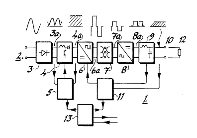
Figure 1 is a block diagram of an AC-DC converter that
belongs to a DC-DC converter, with the voltages
that appeare between the blocks marked out for
simplifying purposes;
Figure 2 is a wiring diagram, significant for the
invention, of the function blocks that pertain
to the invention, with an added power
distributing organ;
Figure 3 is a wiring diagram of a first power
f;I"is5 25 , distributing organ, according to the invention;
::
Figure 4 is a wiring diagram of a second embodiment of
the organ, according to the invention;
Figure 5 is a wiring diagram of a third embodiment of
the power distributing organ;
Figure 6 is a wiring diagram of a fourth embodiment of
the power distributing organ;
Figure 7 is a wiring diagram of a fifth embodiment of
the power distributing organ;
J~O 95/34122 c PCT/SE95/00638
~! 1~7~-~~-
- 13 -
Figure 8 is a wiring diagram of a sixth embodiment of
the power distributing organ;
Figure 9 is a wiring diagram of a seventh embodiment of
the power distributing organ; and
Figure 10 shows the variations in time of a current
through a diode (V3 or V4 according to Fig. 2),
with a circuit arrangement according to Fig. 3,
and somewhat enlarged the variations in time of
the current at one of the switching periods.
DESCRIPTION OF EMBODIMENTS AT PRESENT PREFERRED
With reference to Fig. 1 a block diagram of an AC-DC converter
1 illustrates two connecting conductors that conducts an
alternating voltage and an alternating current. The
alternating voltage, in a previously )mown way, forms a
fullwave rectified voltage on the conductor 3a through a
rectifying bridge 3.
This fullwave rectified voltage reaches a peak value of 375 V
and is connected to a "Roost"-converter 4, which consists of a
coil, a diode and a transistor, where the state of the
transistor is controlled by a control device 5, in a
previously known way, to produce a regulated output voltage
via on the conductors 4a with a value of 380 - 400 VDC, having
a superposed voltage with a double net frequency (100 Hz or
120 Hz), and a peak-to-peak value in the order of 10 V.
The voltage, through the conductors 4a, and the corresponding
current, which will hereafter be denoted as a first direct
voltage, is connected to a converting unit 6, through which a
pulse width modulation provides a first alternating voltage
through the conductor 6a.
.~ VO 95/34122 ~~ (~ PGT/SE95/00638
- 14 -
Further shown, is a first alternating voltage, that occurs on
the conductors 6a, to a second alternating voltage, that occur
on the conductors 7a, transforming unit 7.
The DC-DC converter, significant for the invention, uses the
blocks 6, 7, 8 and 9, where the transforming unit 7 could be
omitted, but is included in order to separate the primary side
of the DC-DC converter from the secondary side in a galvanic
way.
Said first and second alternating voltages are mutually
denoted solely as an alternating voltage, when the
transforming unit 7 is omitted.
The transforming unit 7 can be arranged to transform the
voltage values either up or down, but can also present a
transforming ratio of 1:1.
A second alternating voltage, which cccurs on the conductors
7a, to a second direct voltage, which occurs on the conductors
8a, transforming unit 8, is intended to fullwave rectify the
second alternating voltage on the conductors 7a. The fullwave
rectified pulse shaped direct voltage is connected to a
smoothing filter 9, through the conductors 8a.
fff~.;, 25
~'<;.:~' '
A direct voltage occurs on the output terminals 10 and fed to
a control device 11 at a constant voltage value by means of
phase regulation, through previously known circuits. The
instantaneous current value can be detected through a
detecting connection to the filter 9. The instantaneous value
of the current can be adapted to the instantaneous value of
the load, through required regulation of the current value,
depending on the varying value of the load 12, as the voltage
value is kept constant.
A surveying circuit 13 co-acts with the control devices 5 and
11 in a previously known manner.
JVO 95/34122 PCT/SE95/00638
- 15 -
With reference to Fig. 2, a wiring diagram of a connecting
arrangement shows the transforming unit 6, or inverted
rectifier 6, the transforming unit 7, or the transformer 7,
the converting circuit 8, or the rectifiers 8, and the direct
voltage smoothing filter 9, in order to better illustrate the
inventive thought of the present invention.
Alternating pulse shaped direct voltage related signals 6a,
with an amplitude of approximately 400 VAC, are formed through
an active regulation of the transistors M1 and M4, or M2 and
M3 alternatively, which belong to the inverted rectifier 6, by
means of the control device 11.
In order to understand the present inventive thought it is
important to have an understanding of the course of events
regarding the energy- or power fluctuations at the switching
sequences, the power distribution and the power consumption
during the active time periods.
If it is supposed that the transistors M1 and M4 are given an
active, or conductive, state it is evident that a load current
is fed from the plus-terminal 4a+ through the transistor M1,
the help inductance L1, the capacitance C1, the primary
winding 71 of the transformer 7, and back through the
transistor M4 to the minus terminal 4a-.
Thus the voltage pulse to the transformer 7 is transformed to
the secondary winding 72 of the transformer 7 allowing a
transformed voltage pulse to pass through an inductance L3 and
a diode V4. This pulse is then smoothed through the condenser
C2 and the inductance L4 in order to form a current to the
plus terminal 10+ of conductor 10.
A voltage pulse in the opposite direction is received at the
primary winding 71 during the following switching sequence
when transistors M2 and M3 are in a conductive state, and a
voltage is transformed to the secondary winding 73 to pass
... - 16 - 2~ 6749 4
through an inductance L2 and a diode V3 to generate the required
current to the plus terminal 10+ of conductor 10.
The present invention is intended, at one hand, to as far as
possible limit the back or reverse current that appears through one
of the diodes (V3 and V4 respectively) during the switching
sequences of the transistors M1 to M4.
This can be achieved by using saturable inductances, L2 and
L3, which are dimensioned to limit the back currents through the
adjacent rectifying mean (V3, V4) through high inductance values,
but to appear transparent, by means of saturation, to forward
currents through the same rectifying mean.
In spite of measures that have been taken with inductances that can
be saturated in the aforesaid manner, it has been proven in the
practical application (which is also shown in the time/current
course, according to Fig. 10) that a small back current is still
generated, and that this back current charges the help inductance L1
with a current spike, illustrated in Fig. 10 with the denotations 50
or 51.
Thus, to redistribute a back-current-originating power contribution,
the invention provides a redistributing organ or device A, which
belongings to transforming unit 6, and this organ A is adapted to
redistribute and reduce the losses that occur, for instance, in the
series-connected rectifying means, of the organ A, and in
transistors M1 to M4.
With reference to Fig. 3, it is indicated that organ A consists of a
resistance R1 and two series-connected rectifying means V1, V2, and
that resistance R1 is connected between one connection Lla of the
inductance L1 and the mutual connecting point Va of the two
rectifying means V1, V2.
If a redistributing organ A, according to Fig. 3 and applied to a
wiring diagram according to Fig. 2, is used it is obvious
A
VO 95/34122 ~~ ~ PCT~SE95/00638
- 17 -
that the power stored within the inductance L1 can be
redistributed during the connecting sequence through
resistance R1, by providing a closed circuit, such as through
diode V2, the transistor M1, and the inductance L1.
In particular the invention emphasizes the dimensioning of the
value of the resistance R1.
At a selected practical application the resistance value can
be selected to be approximately 30 ohm.
The selection of the resistance value is, however, very
complex, and requires that consideration be given to various
parameters.
A very low resistance value, in the above described
oscillating circuit (where the resistance R1 is a part),
provides a very long time of discharge for the, as a loss,
contributed power. A high values of the resistance in the
oscillating circuit permits the required power redistribution
and consumption to be performed during a much shorter period
of time.
This condition forms a basic thesis that the value of
resistance R1 is to be selected to be high.
Given this thesis a selected high resistance value, of
resistance R1, will increase the back current related voltage
spikes across the diodes V3 and V4.
Thus, although the resistance value, of resistance R1, must be
high, it must not be so high as to generate a voltage spike
that exceeds a predetermined value, which is the value at
which the diodes V3 and V4 can be destroyed, taking a suitable
safety margin into consideration.
Thus, Fig. 3 illustrates a first embodiment of the power
l0 95134122 ~ ~ PCTISE95I00638
- 18 -
contribution redistributing organ A.
In Fig. 4, a second embodiment of organ A is illustrated. This
embodiment consists of two series-connected rectifying means
V1, V2 and two Zener-diodes, each Zener-diode being counter
connected in series with one of the_rectifying means. The
connection Lla of the inductance is directly connected to the
mutual connecting point Va of the two rectifying means.
Fig. 5 shows that the power contribution redistributing organ
A consists of two series-connected rectifying means V1, V2 and
two Zener diodes Z3, Z4, where the Zener-diodes in principal
can be regarded as being the resistance R1 illustrated in Fig.
3, the Zener diodes being connected in series and counter
connected to each other between one connection Lla of the
inductance Ll and the mutual connecting point Va of the
rectifying means.
Fig. 5 shows a fourth embodiment of an organ A, where
resistance R1, according to Fig. 3, is connected in parallel
with a capacitance C4.
Fig. 7 shows a fifth embodiment of an organ A, using two
series-connected rectifying means V1, V2 and two resistances
~-~~f525 R3, R4, each resistance being connected in series with one of
~~3tsfi
the rectifying means. One connection Lla of the inductance is
directly connected to the mutual connecting point Va of the
two rectifying means.
Fig. 8 shows a sixth embodiment of the power contribution
redistributing organ A, which consists of two series-connected
rectifying means V1, V2 and the primary winding T2p of a
transformer, the primary winding being connected between one
connection Lla of the inductance L1 and the mutual connecting
point Va of the rectifying means.
The secondary winding T2s of the transformer T2 is connected
IO 95/34122 ~ PCT/SE95/00638
- 19
to a rectifying organ 81, and this rectifying organ can be
arranged to form a fullwave rectified voltage, in a previously
known way, on the connections 82.
The rectifying organ 81 can also comprise a voltage smoothing
circuit 81a, in a previously known way. The generated voltage
82 can be directly connected to the load 12 through the
connections 10.
The fullwave rectified voltage 82 can then be connected to the
voltage-smoothing circuit 9 in Fig. 2, without having to use
an internal voltage smoothing circuit.
Fig. 9 shows a seventh embodiment of the organ A, where the
organ consists of two series-connected rectifying means V1,
V2, two resistances R3, R4, each resistance being connected in
series with one of the rectifying means and two capacitances
C5, C6, each being connected in parallel with one of the
resistance R3, R4. One connection Lla cf tha inductance is
directly connected to the mutual connecting point Va of the
two rectifying means.
Although a series connection of a resistance and a diode is
illustrated in Fig. 7 and 9, with a mutual connecting point Va
of the diodes it is obvious that the diodes and the
resistances can change places so that the resistances have a
mutual connecting point Va.
~'he connecting arrangements of the organ A are specifically
suitable with phase regulated full bridges, but the connecting
arrangement can also be used with half bridges, that work with
a constant off-time.
The resistance R1 can be exchanged with a number of other
equivalent circuit connections.
One such example is illustrated in Fig. 9. In this figure the
w CVO 95/34122 ~ ~ ~ PGT/SE95/00638
- 20 -
condensers C5 and C6 are dimensioned so that the voltages
across them are essentially constant. An advantage with this
solution is that it insures that the clamping voltage is
constant, giving good control of the voltage across the output
diodes V3 and V4.
It is also, within the scope of the invention, possible to
exchange the condensers C5 and the resistance R3, as well as
the condensers C6 and the resistance R4 with Zener-diodes to
achieve the same technical effect, which the indicated
connecting arrangements are intended to illustrate.
There are several various embodiments and variations of
connections of the different elements, all within the scope if
the inventive thought, that provide means for transferring
parts of the power losses in the transistors and diodes within
the inverted rectifier 6 to some other component, while same
reducing the total amount of loss.
To connect a power contribution redistributing organ A,
according to the present invention, provides, besides this,
the possibilities to reduce the risk of a self-oscillating
circuit.
s!~;~~;25 The time wise variations of the current through one of the
;;:,:
diodes V3 or V4 are shown in Fig. 10. In this example, a
circuit arrangement, according to Fig. 3, is used. The time
variation at one of the two switching sequences, 50 and 51
respectively, has been somewhat enlarged.
Fig. 10 shows two switching sequences, denoted 50 and 51. The
inductance L2 or L3 is in saturation during the current
variation up to the point "to". Thereafter will the current, at
the switching moment, has the time wise variation which is
illustrated by the curve denoted 5ia. The current spike,
denoted 51b, generates the loss related contributed power that
is to be distributed as previously described.
PCT/SE95/00638
' ~~ VO 95/34122
- 21 -
Supposedly the time variation follows the curve 51c when the
saturable inductances L2, L3 have not been used, resulting in
a larger loss related power contribution.
The inductance L2 or L3 provides a large inductance value
after the time "to", and thereby limits the back current
through the adjacent rectifying mean V3, V4.
The inductances appear transparent to forward currents through
the same rectifying means.
It will be understood that the invention is not restricted to
the illustrated exemplifying embodiments thereof and that
modifications can be made within the scope of the inventive
thought illustrated in the following claims.