Note: Descriptions are shown in the official language in which they were submitted.
~167758
Specification
Title of the Invention
Ignitor
Background of the Invention
The present invention relates to an ignitor
for igniting a target object such as oil and gas.
As a conventional ignitor of this type, there
is a solid-state ignitor whose circuit diagram is shown
in Fig. 8. Referring to Fig. 8, reference symbol VAC
denotes a commercial power supply (AC 100 V); D1, a
diode; Cl and C2, capacitors; Ql, a main transistor; Rl,
a resistor for activating the main transistor Q1; T1, a
transformer; L1, a primary winding of the transformer
T1; L2, a secondary winding of the transformer T1; and
L3, a tertiary winding of the transformer Tl.
In this circuit, the commercial power supply
VAC is rectified and smoothed by the diode Dl and the
capacitor C2, and DC power supply voltage VDC is applied
to a circuit connected to the output stage. By this
power supply voltage VDC, a base current flows via the
resistor Rl to activate the main transistor Q1. A
current flows through the primary winding Ll (primary
side) of the transformer Tl via the main transistor Ql
to generate high voltage in the secondary winding L2
(secondary side) of the transformer Tl, and generate
voltage in the tertiary winding L3 (tertiary side) of
2167758
the transformer Tl. Switching between the ON and OFF
states of the main transistor Q1 is repeated using the
output from the tertiary side as a control output. When
the main transistor Q1 is switched, an LC resonant
circuit constituted by the capacitor C1 and the coil Ll
resonates to repeatedly generate high voltage on the
secondary side of the transformer Tl. By the high
voltage generated on the secondary side of the
transformer Tl, a spark is generated at a gap between
high-voltage terminals TEl and TE2 to ignite a target
object with this spark.
In the conventional solid-state ignitor
described above, however, the following problems arise
due to decreases in ambient temperature and power supply
voltage VDC-
[Decrease in Ambient Temperature]
As a general characteristic, a decrease in
ambient temperature decreases a current gain (hFE) of the
main transistor Ql, thereby decreasing a collector
current Il in the main transistor Q1, and also an output
current I2 on the secondary side of the transformer T1.
For this reason, when the ambient temperature decreases,
an output energy is also decreased, and the amount of
discharge energy required for igniting a target object
is difficult to obtain, thus degrading ignition
properties.
21~7758
When liquid such as oil is used as a target
object, the liquid such as oil gels at a low
temperature. Oil particles to be sprayed from a nozzle
become larger to make ignition more difficult. In
particular, when used at an ambient temperature of 0~C
or less, an ignition delay or an ignition miss of the
ignitor with respect to a target object frequently
occurs.
[Decrease in Power Supply Voltage VDC]
A decrease in power supply voltage VDC
decreases voltage VCE across the collector and emitter of
the main transistor Ql. LC resonant voltage across the
capacitor C1, and output voltage on the secondary side
of the transformer T1 are also decreased. In addition,
the decrease in LC resonant voltage decreases output
voltage on the tertiary side of the transformer T1 to
decrease a base current IB for the main transistor Q1.
For this reason, the ON time width is narrowed in
switching the main transistor Q1, and the collector
current Il in the main transistor Q1 is decreased to
decrease the output current I2 on the secondary side of a
transformer T2.
More specifically, when the power supply
voltage VDC decreases, both the output voltage and
current on the secondary side of the transformer T2 are
decreased, and an output energy is reduced. A discharge
energy required for igniting a target object is
~167758
difficult to obtain, degrading ignition properties. In
particular, when the ignitor is used under the
environment where the commercial power supply VAC greatly
varies, e.g., in a factory, an ignition delay and an
ignition miss frequently occur.
Summary of the Invention
It is an object of the present invention to
provide an ignitor having good ignition properties with
respect to a decrease in ambient temperature.
It is another object of the present invention
to provide an ignitor having good ignition properties
with respect to a decrease in power supply voltage.
In order to achieve the above objects,
according to the present invention, there is provided an
ignitor comprising a first transistor which is activated
in accordance with supply from a DC power supply to
perform switching; a transformer having a primary
winding through which a switching current flows via the
first transistor, a secondary winding for generating
high voltage when the switching current flows through
the first winding, and a tertiary winding for generating
a control output for controlling the switching of the
first transistor in accordance with the high voltage
generated in the secondary winding; ignition means for
igniting a target object using the high voltage
generated in the secondary winding of the transformer;
and switching control means for prolonging an ON time
CA 021677~8 1998-08-18
for the switching of the first transistor to compensate for
a decrease in igniting energy due to a decrease in at least
one of an ambient temperature and power supply voltage using
said control output from said tertiary winding.
Brief Description of the Drawings
FigO 1 is a circuit diagram showing a solid-state
igniter according to Embodiment 1 of the present invention;
Figs. 2A to 2D are timing charts for explaining the
operations of the solid-state igniter shown in Fig. 1 when
the ambient temperature and the power supply voltage
decrease;
Figs. 3A and 3B are graphs showing the temperature
characteristics and power supply voltage characteristics of
the solid-state igniter shown in Fig. 1, respectively;
Fig. 4 is a circuit diagram showing a solid-state
igniter according to Embodiment 2 of the present invention;
Figs. 5A to 5G are timing charts showing the
operations of an activation pulse generation section in the
solid-state igniter shown in Fig. 4;
Figs. 6A to 6I are timing charts for explaining the
operations of the solid-state igniter shown in Fig. 4 when
the ambient temperature and the power supply voltage
decrease;
Figs. 7A and 7B are graphs showing the temperature
characteristics and power supply voltage
~1677~g
characteristics of the solid-state ignitor shown in
Fig. 4, respectively; and
Fig. 8 is a circuit diagram showing a
conventional solid-state ignitor.
Description of the Preferred Embodiments
An ignitor of the present invention will be
described below with reference to the accompanying
drawings.
[Embodiment 1]
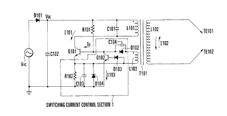
Fig. 1 shows a solid-state ignitor according
to an embodiment of the present invention. Referring to
Fig. 1, reference symbol VAC denotes a commercial power
supply (AC 100 V) one terminal of which is connected to
a signal ground; D101, a rectifying diode connected in
series with the commercial power supply VAC; C102, a
smoothing capacitor connected parallel to the circuit
obtained by connecting the commercial power supply VAC
and the diode D101 in series with each other; Q101, a
main transistor; R101, a resistor connected between one
20 terminal of a capacitor C101 and the base of the main
transistor Q101 to activate the main transistor Q101;
T101, a transformer; L101, a primary winding of the
transformer T101 which is connected between one terminal
of the capacitor C101 and the collector of the main
transistor Q101; L102, a secondary winding of the
transformer T101 having both terminals connected to
high-voltage terminals TE101 and TE102, respectively;
21677~g
and L103, a tertiary controlling winding of the
transformer T101. Reference numeral 1 denotes a
switching current control section connected between the
main transistor Q101 and the transformer T101. The
switching current control section 1 for controlling a
switching current in the main transistor Q101 is added
to the conventional solid-state ignitor shown in Fig. 8
to obtain the ignitor of Embodiment 1.
The switching current control section 1 is
constituted by a sub-transistor Q102, a resistor R102,
diodes D102 to D104, and capacitors C103 and C104. In
the switching current control section 1, the collector
of the sub-transistor Q102 iS connected to the base of
the main transistor Q101, the base of Q102 is connected
to the emitter of the main transistor Q101 via the diode
D103, and the emitter is connected to the signal ground.
The emitter of the main transistor Q101 is connected to
the signal ground via the resistor R102. The capacitor
C103 and the diode D104 are connected parallel to the
resistor R102. A circuit obtained by connecting the
diode D102 and the capacitor C104 parallel to each other
is connected between the base of the main transistor
Q101 and one terminal of the tertiary winding L103 of
the transformer T101. The other terminal of the
tertiary winding L103 of the transformer T101 is
connected to the emitter of the main transistor Q101.
21677~8
The diode D102 and the capacitor C104 adjust a
base current which flows through the main transistor
Q101. The capacitor C104 mainly contributes to good
rising of the base current for the main transistor Q101,
while the diode D102 supplies the base current for the
main transistor Q101 for a predetermined period of time
or more. In addition, the capacitor C103 adjusts the ON
timing for the sub-transistor Q102, while the diode D104
causes the main transistor Q101 to oscillate stably.
In Embodiment 1, an npn bipolar transistor
having a current gain hFE ~f 10 to 50, and an npn bipolar
transistor having a current gain hFE of 200 or more are
used as the main transistor Q101 and the sub-transistor
Q102, respectively. As general characteristics, a
decrease in ambient temperature decreases the current
gains hFE ~f the transistors Q101 and Q102. Further, as
general characteristics, voltage drops across the diodes
D103 and D104 also become large with a decrease in
ambient temperature.
In this circuit, the commercial power supply
VAC is rectified and smoothed by the diode D101 and the
capacitor C102, and DC power supply voltage VDC is
applied to a circuit connected to the output stage. By
this power supply voltage VDC~ a base current flows via
the resistor R101 to activate the main transistor Q101.
A current flows through the primary winding L101
(primary side) of the transformer T101 via the main
2167758
transistor Q101 to generate high voltage in the
secondary winding L102 ( secondary side) of the
transformer T101, and generate voltage in the tertiary
winding L103 (tertiary side) of the transformer T101.
5 Switching between the ON and OFF states of the main
transistor Q101 is repeated using the output from the
tertiary side as a control output. When the main
transistor Q101 is switched, an LC resonant circuit
constituted by the capacitor C101 and the coil L101
resonates to repeatedly generate high voltage on the
secondary side of the transformer T101. BY the high
voltage generated on the secondary side of the
transformer T101, a spark is generated at a gap between
a pair of high-voltage terminals TE101 and TE102 having
15 a predetermined interval therebetween to ignite a target
object with this spark.
Figs. 2A to 2D explain the operation states of
the activated circuit shown in Fig. 1, in which Fig. 2A
shows base-emitter voltage VBE in the main transistor
20 Q101, Fig. 2B shows a base current IB in the main
transistor Q101, Fig. 2C shows a collector current I
in the main transistor Q101, and Fig. 2D shows a
collector current Il03 in the sub-transistor Q102. Note
that, in each of Figs. 2A to 2D, a waveform indicated by
25 a solid line exhibits the case of a low ambient
temperature or low power supply voltage VDC, and a
waveform indicated by a dotted line exhibits the case of
~ ~77~8
a normal ambient temperature or normal power supply
VO1tage VDC-
In the circuit shown in Fig. 1, when the power
supply voltage VDC is applied, the base current IB flows
through the main transistor Q101 via the resistor R101
tFig. 2B) to turn on the main transistor Q101. Upon the
ON operation of the main transistor Q101, the collector
current I1ol flows (Fig. 2C) to generate a potential
difference across the resistor R102. When this
potential difference increases to a predetermined value
or more, the diode D103 is turned on, and a base current
flows through the sub-transistor Q102 to turn on the
sub-transistor Q102. Upon the ON operation of the
sub-transistor Q102, the collector current Il03 flows
(Fig. 2D) to shunt the base current IB in the main
transistor Q101. The base current IB in the main
transistor Q101 changes in accordance with output
voltage from the tertiary winding L103 of the
transformer T101. When the output voltage from the
tertiary winding L103 of the transformer T101 increases
(rises), the base-emitter voltage VBE is generated in the
main transistor Q101 (time tl shown in Fig. 2A) to turn
on the main transistor Q101. When the output voltage
from the tertiary winding L103 of the transformer T101
decreases (drops), the base current IB is decreased
(Fig. 2B), and the base-emitter voltage VBE in the main
-- 10 --
2167758
transistor Q101 is decreased (time t2 shown in Fig. 2A)
to turn off the main transistor Q101.
~Decrease in Ambient Temperature]
A decrease in ambient temperature decreases
not only the current gain hFE of the main transistor Q101
but also the current gain h~E of the sub-transistor Q102.
The collector current Il03 as a shunted current in the
sub-transistor Q102 is decreased (Fig. 2D). In
addition, since a voltage drop in the diode D103 becomes
large at a low temperature, the collector current Il03 in
the sub-transistor Q102 is further decreased. The base
current IB in the main transistor Q101 is increased
(Fig. 2B) to prolong the ON time (period TW shown in
Fig. 2A) from TWl indicated by a dotted line to TWz
indicated by a solid line in switching (ON/OFF driving)
the main transistor Q101. For this reason, the
collector current Ilo1 in the main transistor Q101 is
increased (Fig. 2C) to compensate the decrease in output
current Il02 in the secondary winding L102 of the
transformer T101 due to the decrease in the main
transistor Q101.
In Embodiment 1, the primary winding L101 of
the transformer T101 and the capacitor C101 resonate to
transfer energy to the secondary side. When the ON
width of the main transistor Q101 is widened due to a
decrease in ambient temperature, resonant and output
voltages slightly increase because oscillation can be
2~677~8
performed around a resonant frequency. Therefore, a
decrease in output current Il02 with a decrease in
ambient temperature is excessively compensated. When
the ambient temperature decreases, the output current
Il02 equal to or more than an output current at a normal
ambient temperature can be obtained. That is, as
represented by ambient temperature-output energy
characteristics (temperature characteristics) in
comparison with the prior art in Fig. 3A, as the ambient
temperature becomes lower, the output energy becomes
larger, preventing degradation in ignition properties
due to a decrease in ambient temperature.
[Decrease in Power Supply Voltage VDC ]
As has been explained in the prior art, a
decrease in power supply voltage VDC decreases output
voltage from the tertiary winding L103 of the
transformer T101. The base current IB to the main
transistor Q101 is decreased to decrease the collector
current Ilol in the main transistor Q101. When the
collector current Ilol in the main transistor Q101 is
decreased, a voltage drop in the resistor R102 becomes
small, the base-emitter voltage VBE in the sub-transistor
Q102 is decreased, and the collector current Il03 as a
shunted current in the sub-transistor Q102 is decreased
(Fig. 2D). The base current IB in the main transistor
Q101 is increased (Fig. 2B) to prolong the ON time
(period TW shown in Fig. 2A) from TWl indicated by the
~67758
dotted line to TW2 indicated by the solid line in
switching (ON/OFF driving) the main transistor Q101.
For this reason, the collector current Ilol in the main
transistor Q101 is increased (Fig. 2C) to compensate the
decrease in output current Il02 in the secondary winding
L102 due to the decrease in output voltage from the
tertiary winding L103 of the main transistor Q101.
Further, in Embodiment 1, the primary winding L101 of
the transformer T101 and the capacitor C101 resonate to
transfer energy to the secondary side. When the ON
width of the main transistor Q101 is widened (power
supply voltage is decreased), resonant and output
voltages slightly increase because oscillation can be
performed around a resonant frequency. When the ON
width of the main transistor Q101 is narrowed (power
supply voltage is increased), the resonant and output
voltages slightly decrease because oscillation is
performed at a frequency slightly shifted from the
resonant frequency. That is, the circuit operates so as
to keep the peak value of output voltage constant.
Fig. 3B shows power supply voltage-output
energy characteristics (power supply voltage
characteristics) in this case in comparison with the
prior art. In this manner, according to Embodiment 1,
the degree of a decrease in output energy is small with
respect to a decrease in power supply voltage VDC I
CA 021677~8 1998-08-18
thereby preventing degradation in ignition properties due to
the decrease in power supply voltage VDC.
[Embodiment 2]
Fig. 4 shows a solid-state ignitor according 5 to
another embodiment of the present invention. In Embodiment
2, a field effect transistor (FET) is used as a main
transistor Q201. An activation pulse generation section 2
for generating an activation pulse, and a pulse width
control section 3 for controlling the pulse width of
switching voltage are arranged. Resistors R203 to R206,
capacitors C205 and C206, a diode D205, and Zener diodes
ZD201 and ZD202 are arranged in addition to a diode D201 and
a capacitor C202 in a rectifying/smoothing section 4.
The activation pulse generation section 2 is
constituted by a transistor Q202, resistors R207 to R214,
capacitors C207 and C208, diodes D206 and D207, inverters
INVl to INV3, and a Zener diode ZD203. The pulse width
control section 3 is constituted by the transistor Q202, a
transistor Q203, resistors R213 to R217, a capacitor C209,
diodes D208 to D210, inverters INV3 to INV6, and Zener
diodes ZD204 to ZD206. Note that the transistor Q202, the
resistors R213 and R214, and the inverter INV3 are commonly
used for the activation pulse generation section 2 and the
pulse width control section 3.
In the pulse width control section 3, a CR time
constant circuit 5 is constituted by the capacitor C209 and
the resistor R215. Voltage Val which changes in accordance
- 14 -
CA 021677~8 1998-08-18
with power supply voltage VDC via the Zener diodes ZD204 and
ZD205 is applied to one terminal of the CR time constant
circuit 5 on the resistor R215 side. Voltage which changes
between "L" and "H" levels in accordance with voltage on the
tertiary side of a transformer T201 via the inverter INV4 is
applied to the other terminal of the CR time constant
circuit 5 on the capacitor C209 side.
In Embodiment 2, a capacitor such as a ceramic
capacitor which increases in capacitance with a decrease in
temperature is used as the capacitor C209. As the Zener
diode ZD205, a diode having Zener voltage of 5.1 V or less
is used in which a decrease in temperature increases the
Zener voltage. As the Zener diode ZD204, a diode is used in
which a decrease in temperature increases forward voltage.
In the circuit shown in Fig. 4, a commercial power
supply VAC is rectified and smoothed by the diode D201 and
the capacitor C202, and is applied as DC power supply
voltage VDC to a circuit connected to the output stage. Upon
receptïon of the power supply voltage VDCI waveforms change
at points P201 to P206 in the activation pulse generation
section 2, as shown in Figs. 5A to 5F. A one-shot pulse
shown in Fig. 5F is supplied to the gate of the FET Q201.
By the one-shot pulse, the FET Q201 is activated to cause a
current I201; to flow (Fig. 5G). A current flows through a
primary winding L201 (primary side) of the transformer T201
via the FET Q201 to generate high voltage in the secondary
winding L202 (secondary side) of the transformer T201.
- 15 -
CA 021677~8 1998-08-18
On the other hand, voltage is also generated in a
tertiary winding L203 (tertiary side) of the transformer
T201~ The FET Q201 is continuously switched using an output
from the tertiary side as a control output via the pulse
width control section 3. A capacitor C201 and the coil L201
LC-resonate to repeatedly generate high voltage on the
secondary side of the transformer T201. By this high
voltage, a spark is generated between high-voltage terminals
TE201 and TE202 to ignite a target object with this spark.
Figs. 6A to 6H show waveforms at points P207 to P214
in the pulse width control section 3, respectively, and Fig.
6I shows the current I201 flowing through the FET Q201. Note
that, in each of Figs. 6E to 6I, a waveform indicated by a
solid line exhibits the case of a low ambient temperature or
low power supply voltage VDCI and a waveform indicated by a
dotted line exhibits the case of a normal ambient
temperature or normal power supply voltage VDC.
In the pulse width control section 3, an output from
the tertiary side of the transformer T201 appears as a
control output at the point P207 (Fig. 6A). By the control
output~ the transistor Q203 is switched to generate voltage
at the point P208 at "L"/"H" level in accordance with the
ON/OFF state of the transistor Q203 (Fig. 6B). The voltage
at the point P208 is applied to the inverter INV5 and
inverted (Fig. 6C), and further inverted by the inverter
INV4 (Fig. 6D). The resultant voltage is applied to the
- 16 -
CA 021677S8 1998-08-18
other terminal of the CR time constant circuit 5 on the
capacitor C209 side.
On the other hand, the voltage Va1 which changes in
accordance with the power supply voltage VDC via the Zener
diodes ZD204 and ZD205 is applied to one terminal of the CR
time constant circuit 5 on the resistor R215 side. When the
other terminal side of the CR time constant circuit 5 goes
to "L" level, a charging current flows from one terminal
side of the CR time constant circuit 5 to the capacitor C209
to inc~ease voltage across the capacitor C209 (Fig. 6E).
When the voltage across the capacitor C209 reaches a
predetermined value after a lapse of time based on the time
constant of the CR time constant circuit 5, i.e., a
potential at the point P211 reaches a predetermined value
(time tl shown in Fig. 6E), an output from the inverter INV6
is inverted to "L" level (time tl shown in Fig. 6F). An
output from the inverter INV3 is also inverted to "H" level
(time tl shown in Fig. 6G). The transistor Q202 is turned
on by an output of "H" level from the inverter INV3, and
gate voltage to the FET Q201 drops to "L" level (time tl
shown in Fig. 6H). The FET Q201 is turned off to interrupt
the current I201 flowing through the FET Q201 (time tl shown
in Fig. 6I).
[Decrease in Ambient Temperature]
When the ambient temperature decreases, the
capacitance of the capacitor C209 in the CR time constant
circuit 5 is increased to increase the time constant of the
- 17 -
CA 021677~8 1998-08-18
CR time constant circuit 5. In addition, the Zener voltage
of the Zener diode ZD205 and the forward voltage of the
Zener diode ZD204 are increased to decrease the voltage V
to be applied to one terminal of the CR time constant
circuit 5O Since the rate of increase of charging voltage
for the capacitor C209 becomes low, a time required for
increasing voltage across the capacitor C209 to a
predetermined value is prolonged to interrupt the current
I201 flowing through the FET Q201 at time t2 after time tl
shown in Fig. 6E.
When the ambient temperature decreases, the
switching pulse width (period TW shown in Fig. 6H) in
switching the FET Q201 is widened from TWl indicated by a
dotted line to TW2 indicated by a solid line. That is,
since the ON time in ON/OFF-driving the FET Q201 is
prolonged from TWl to TW2 to increase a drain current
~167758
flowing through the FET Q201, a decrease in drain
current due to an increase in threshold voltage across
the gate and source of the FET Q201, and the like can be
suppressed to compensate a decrease in output current
Izoz
In Embodiment 2, a decrease in output current
Izoz with a decrease in ambient temperature is
excessively compensated. When the ambient temperature
decreases, the output current I202 equal to or more than
an output current at a high ambient temperature can be
obtained. That is, as represented by ambient
temperature-output energy characteristics (temperature
characteristics) in comparison with the prior art in
Fig. 7A, as the ambient temperature becomes lower, the
output energy becomes larger, preventing degradation in
ignition properties due to a decrease in ambient
temperature.
[Decrease in Power Supply Voltage VDC ]
When the power supply voltage VDC decreases,
voltage Va to be applied to the anode of the Zener diode
ZD204 is decreased to decrease the voltage Val to be
applied to one terminal of the CR time constant circuit
5. Since the rate of increase of charging voltage for
the capacitor C209 becomes low, a time required for
increasing voltage across both the terminals of the
capacitor C209 to a predetermined value is prolonged to
-- 19 --
~167758
interrupt the current I201 flowing through the FET Q201
at time t2 after time tl shown in Fig. 6E.
When the power supply voltage VDC decreases,
the switching pulse width (period TW shown in Fig. 6H)
in switching the FET Q201 is widened from TWl indicated
by the dotted line to TWz indicated by the solid line.
That is, since the ON time in ON/OFF-driving the FET
Q201 is prolonged from TWl to TW2, a current flowing
through the FET Q201 is increased to compensate a
decrease in output current I202 due to a decrease in
output voltage from the tertiary side of the transformer
T201.
Fig. 7B shows power supply voltage-output
energy characteristics in this case in comparison with
the prior art. In this manner, according to Embodiment
2, the decrease amount of output voltage with a decrease
in power supply voltage VDC is also compensated by the
increase amount of the output current Iz02. An output
energy is kept constant with respect to the decrease in
power supply voltage VDC~ thereby preventing degradation
in ignition properties due to the decrease in power
supply voltage VDC-
As has been apparent from the abovedescription, according to the present invention, when
the ambient temperature or the power supply voltage
decreases, the ON time in switching a main transistor is
prolonged to increase a current flowing through the
- 20 -
21677S8
primary side of a transformer via the main transistor.
Therefore, a decrease in output energy on the secondary
side of the transformer is compensated. Good ignition
properties can be obtained with respect to decreases in
ambient temperature and power supply voltage.
- 21 -