Note: Descriptions are shown in the official language in which they were submitted.
~ ~80 0~
TAPER SHAPES FOR ULTR~LOW sTnF.T.oR~. LEVELS
IN DIRECTIONAL COUPLER FILTERS
Field of Invention
This invention relates to directional coupler
filters and more particularly to such filters wherein the
spacing between the waveguides is tailored to maximize
sidelobe suppression and to minimize bandwidth.
Background of Invention
The potential communication capacity of optical
fibers operating in the low loss wavelength windows of
1.3 um and 1.5 um is in the order of tens of Terahertz.
The practical utilization of this bandwidth may be realized
through the use of wavelength division multiplexing (WDM).
In this scheme the spectral range is subdivided and
allocated to different carrier wavelengths (channels) which
are multiplexed onto the same fiber. The frequency
bandwidth that an individual channel occupies depends on a
number of factors, including the impressed modulation
bandwidth, margins to accommodate for carrier frequency
drift and carrier frequency uncertainty, and also to reduce
possible cross-talk between channels.
Although the isolated optical fiber may
inherently have tremendous information carrying capacity,
the overall optical communication link may be significantly
restricted in bandwidth. These restrictions may result
from the limited optical amplifier spectral windows, the
availability of lasing sources and their tuning ranges, and
also filter tuning ranges. Hence, to achieve efficient use
of bandwidth requires that the available communications
windows be densely filled with multiplexed channels. At
the output of such a system, filters are needed to separate
the wavelength channels. The performance of these
wavelength filters in their ability to reject out of band
signals, critically determines channel spacing and hence
channel density.
s~ ~ r~
8 0 ~ ~
The type of filters of interest here operate
through a wavelength dependent exchange of power between
two waveguide modes. It is well known that two waveguides
placed in close proximity may exchange power through their
evanescent fields, which penetrate the guiding layer of the
other waveguide. This power exchange occurs continuously
along the propagation direction, with a rate determined by
the inter-waveguide spacing and the degree of velocity-
matching of the two modes. If the velocities of the two
waveguide modes are identical, the situation is termed
'synchronous' or 'phase matched', and the power coupled
into one of the waveguides accumulates constructively.
Complete power exchange is then possible and occurs at a
characteristic coupling length LC which is determined by
the structure of the device. If the modes propagate at
different velocities, then this condition is termed 'non-
phase matched' or 'asynchronous'. The power in the coupled
waveguide accumulates with a phase error, leading to
incomplete power transfer in this case. The larger the
phase-mismatch, the faster the phase-error accumulates,
which results in less power being transferred to the
coupled waveguide.
FIGURE la shows two typical waveguides placed in
parallel, a configuration known as the directional coupler.
The input power is initially launched into waveguide 1 (the
'input' guide), and the output is extracted from guide 2
(the 'coupled' guide). FIGURE lb shows the power in
waveguide 2 (the 'coupled' guide) as a function of device
length for two cases of phase-matching. The solid curve
represents a synchronous case, with complete power exchange
occurring at Lc = 5mm. The dashed curve represents
coupling between asynchronous modes.
Wavelength selectivity in the directional coupler
occurs through differential velocity dispersion. At the
design wavelength, the velocities of the two modes are
equal. As the wavelength is changed or 'detuned', the mode
velocities necessarily change. For filtering action
,,,~
2~ ~8Q ~
however, it is critical that the difference between these
mode velocities changes, i.e., a differential velocity
dispersion is required. The rate of change of differential
velocity with respect to wavelength is the primary factor
in determining filter bandwidth. This rate is a function
of material type and waveguide structure. FIGURE 2 shows
the filter response of a parallel directional coupler. The
abscissa is in terms of a normalized detuning factor, ~,
which is a measure of the velocity difference between the
coupled modes. This axis can be converted into an actual
wavelength scale when the relationship between ~ and
wavelength ~, is established for a particular device. The
ordinate is the power in the coupled waveguide, in
logarithmic scale, for a device of fixed length. The
15 ~ normalized half-power bandwidth is 8.4 radians (rad), and
the maximum sidelobe level is at -9.3 db.
For optical communications purposes, a sidelobe
level of -9.3 db is too large, since it would represent a
significant cross-talk to an adjacent wavelength channel,
if these channels were spaced by the width of the passband.
If it is required that the cross talk in an adjacent
channel be less than -9.3 db, the spacing between adjacent
channels in the wavelength domain must be made much larger
than the main passband width. Since the sidelobe levels
decrease at a slow rate with detuning (see FIGURE 2), the
channels must be widely separated. Hence, a severe penalty
is paid in terms of channel density, and hence information
carrying capacity, for the price of low cross-talk. It is
very desirable then to identify some degree of freedom
which may be used to improve filter response.
The degree of freedom most commonly used in
directional couplers is a modulation of the interaction
strength of the two coupled modes. This may be achieved
for example, by modulating the inter-waveguide separation
in the directional coupler. In many other branches of
optics and physics this process is known as 'apodization'.
In waveguide theory it is referred to as 'tapering'.
Q ~
Directional coupler devices are commonly modeled
through a set of coupled differential equations such as:
d = -jke~j~ZA2 Equation (la)
= -jkei~Z~ Equation (lb)
dz
In (la) and (lb) ~ and A2 represent the amplitudes in
waveguides 1 and 2. ~ is the detuning constant and k is
the interaction strength. k depends on the waveguide
structure and is strongly influenced by the separation
between adjacent waveguides. The physical origin of this
coupling may be due to the interaction of evanescent fields
in a uniform coupler,- (as in FIGURE la), or coherent
scattering in a grating-assisted coupler.
By varying the interaction strength k along the
directional coupler, the spectral response of the device
may be improved. The physical origin of this improvement
is in the interferometric nature of the coupling process:
at every position along the coupler, power is being
transferred from the input waveguide to the coupled
waveguide. The total power in the coupled waveguide at
some point then, is an interferometric sum of all the power
coupled into the waveguide prior to that point. That is, a
sum including relative phase delays. By adjusting the
interaction strength k along the waveguide, one dictates
the rate of power transfer at each position, along with its
phase relationship to the total coupled power. By
judicious choice of the coupling taper shape k(z), it is
theoretically possible to generate any (passive) response.
How to calculate the taper shape k(z) for a
desired response has been a long standing unanswered design
question. The original proposal, suggested in 1978 by
Alferness et al, IEEE J. Quantum Physics, QE-14, No. 11,
1978, pp. 843-847, was based on an approximate Fourier
transform relation which gave a few promising shapes. This
k
Q ~
proved to be a useful guideline in improving actual device
response (Alferness, Applied Physics Letters, Vol. 35, No.
3, 1979, pp. 260-262), but thus far has been unsuccessful
in yielding the sidelobe suppression required in
communication systems. To date no improvements have been
advanced, and the same shapes suggested in 1978 continue to
be the only ones analyzed (see, for example, H. Sakata,
Optical Letters, Vol. 17, No. 7, 1992, pp. 463-465).
The goal of filter design is to solve for the
interaction function k(z) of (1), given some desired output
response as a function of wavelength A2(~). However, when
k(z) is non-constant, the set of coupled equations in (1)
has no analytic solution in general. Hence, filter design
is currently guided by a set of approximate solutions. The
most important of these approximate solutions is the
Fourier transform relation, given by:
A2(~) # ¦k(z)e~j~Zdz Equation (2)
In Equation (2), A2(4B) is the amplitude in the output or
coupled waveguide as a function of detuning ~, (which may
be related to the actual wavelength ~). Because Equation
(2) represents a Fourier transform relation between k(z) in
the spatial domain and A2(~) in the wavelength domain, the
principle of duality may be used. That is, given a desired
A2(~), k(z) is found by the inverse Fourier transform.
This approximation is valid for small coupling values, and
does not extend to describe the critical region of the main
passband and first few sidelobes. No analytic solution
currently treats the important region around the central
wavelength.
Summary of the Invention
The present invention seeks to produce a
directional coupler filter having a specific sidelobe
level.
'~ ~
The present invention also seeks to produce a
directional coupler filter having a specific sidelobe level
and a minimum spectral bandwidth for the specific sidelobe
level.
The present invention seeks to produce the
aforementioned directional coupler filter by specifying an
interaction strength function between waveguides.
The present invention seeks to produce the
specified interaction strength by defining the shape
function between the waveguides.
Therefore in accordance with a first aspect of
the present invention there is provided a directional
coupler filter comprising a first waveguide for receiving
an optical signal having at least one predetermined
wavelength and a second waveguide in a spaced relationship
to the first waveguide so that the predetermined wavelength
is selectively coupled from the first waveguide to the
second waveguide. The spaced relationship is tailored to
provide an interactive strength therebetween in accordance
with the formula
k(z) = Lo (z) + SL,(z) + 52L2(z) + S3L3(z)
where k(Z) = interactive strength,
S = sidelobe level in ~, and
Lo~Ll~L2~L3~--- are functions of the
propagation distance (z)
so as to suppress spectral sidelobes of the coupled
wavelength to a level down to -75 db.
In a preferred embodiment the spectral bandwidth
is a minimum for the selected sidelobe.
In accordance with a second aspect of the present
invention there is provided a method of suppressing the
sidelobe levels in an optical directional coupler filter
having a first waveguide to receive an optical signal
having at least one predetermined wavelength and a second
_ . --
Q ~ ~
waveguide in spaced relationship to the first waveguide,
the predetermined wavelength being selectively coupled to
the second waveguide, the method comprising tailoring the
spaced relationship between the first and second waveguides
so as to provide an interactive strength according to the
formula:
k(z) = Lo(z)+ SL,(z) +S2L2(z)+ S3L3(z)
wherein
k(z) = normalized interactive strength,
S = desired sidelobe level in ~, and
Lo,LI.. .....are functions of propagation distance (z).
Brief Description of Drawings
The invention will now be described in greater
detail with reference to the appended drawings wherein:
FIGURE la is a plan view of a directional coupler
having parallel (non-tapered) waveguides;
FIGURE lb shows the power in the coupled
waveguide as a function of propagation distance for
synchronous and asynchronous designs;
FIGURE 2 illustrates graphically the spectral
response of a parallel coupler;
FIGURE 3 shows the filter bandwidth as a function
of the highest sidelobe level;
FIGURE 4a shows coupling strength as a function
of normalized propagation distance for an optimum coupler
with -60 db sidelobes;
FIGURE 4b is the spectral response for the filter
of FIGURE 4a;
FIGURE 4c is the spectral response of a physical
device simulated with the beam propagation numerical method
(BPM) and using the shape of FIGURE 4a;
FIGURE 4d illustrates physical separation between
two adjacent waveguides for the BPM simulation of FIGURE
4c;
~ ~ ~ 8 ~ Q
FIGURE 5 shows taper shapes of -40 db, -50 db and
-75 db couplers generated in accordance with the formula of
the present invention;
FIGURES 6a, 6b and 6c show spectral responses of
the couplers of FIGURE 5 - for -40 db, -50 db and -75 db
respectively;
FIGURE 7 illustrates the bandwidth/sidelobe level
relationship for a coupler designed in accordance with the
present invention and the theoretical optimum;
FIGURE 8 is a plan view of a practical embodiment
of the present invention;
FIGURE 9 is a plan view of the coupler of FIGURE
8 having gratings to assist the coupling; and
FIGURE 10 is a plan view of the device of FIGURE
8 having electrodes for electro-optic tuning.
Detailed Description of the Invention
As stated the objective herein is to produce
filters with a specific sidelobe level. The response of
the coupler in between sidelobes is unimportant, since by
definition the sidelobes represent local extrema. If we
have some coupler shape ko(z), then the following error
vector is defined:
E(ko) = [Eo(ko~l(ko~ ~m(ko)] Equation (3)
The components ~j, {i=l...m} describe the error
between the desired sidelobe level and the current sidelobe
level for shape ko~ for each of the m sidelobes
considered: ~; = (~j-pj), where ~j is the desired sidelobe
level and Pi is the current sidelobe level for sidelobe i.
We let the arbitrary coupling coefficient be
represented as k(z) = ~ Nanfn(z), where the fn is an
arbitrary set of functions. The unknowns are the
coefficients an which are written in a vector,
k = (al,a2,...aN). Given an initial state ko~ an improvement
~ ~ r
to ko denoted by k = ko +~k is found by evaluating the
incremental improvement vector ~k,
~k = ~J (JJ ) E(ko) Equation (4)
where Jij = ~k is the Jacobian, and ~ is a scaling
parameter used to decelerate the convergence. Equation (4)
is repeatedly applied until a satisfactory optimization is
achieved. Hence the optimum value is analytically given by
the function k(z) = ~anfn(z).
Achieving the desired sidelobe level is the first
criteria in filter synthesis. The second criteria is to
obtain the narrowest bandwidth while still maintaining the
m~x;mum tolerable sidelobe level. This second criteria is
met when all sidelobe levels are at the maximum tolerable
level. This may be proved rigorously in the following way.
Define the coupler bandwidth B, as a function of the
levels of all the sidelobes: B = B(sl,s2, S3,.. .) where sj is
the absolute value of sidelobe j. Evaluate the gradient of
B with respect to the vector S = (s"s2,s3,...),
W(s) = VsB (~ &2 ) Equation (5)
W(s) is numerically shown to be positive definite,
indicating that decreasing any sidelobe has the effect of
increasing the bandwidth B. Hence for a desired maximum
sidelobe level x, all sidelobes must be below x by
definition, but to achieve the minimum bandwidth, they
should only be infinitesimally below x.
Using the above method, a coupler with
arbitrarily low sidelobes may be theoretically generated.
Before actual shapes are presented for various couplers,
the overall achievements are compared to currently known
taper functions. In FIGURE 3, the trade off between the
''
desired sidelobe level (abscissa) and the bandwidth at that
level (ordinate) is shown. The solid curve represents the
theoretical results derived here. This represents the
narrowest possible bandwidth at a desired sidelobe level, a
coupler cannot have a response that lies below this line.
For comparison, the response of a few of the well known
shapes are plotted as labeled points. The best known
couplers have a maximum sidelobe level in the range of -40
db to -45 db. On the other hand, the method presented here
may generate couplers with sidelobe levels several orders
of magnitude lower.
A representative result of using Equations (3)
and (4) for filter synthesis is given in FIGURE 4a, which
shows the optimum shape of k(z) for a coupler designed for -
60 db sidelobes. The abscissa is in normalized lengthunits. The actual physical length of the device is
obtained by multiplying the abscissa in FIGURE 4a by the
coupling length LC, of the specific device. The ordinate
is the strength of k(z) in normalized units. k(z) may be
translated into either inter-waveguide spacing or grating
strength, in a specific uniform coupler or grating-assisted
coupler, respectively. FIGURE 4b shows the theoretical
spectral response of the taper shape of FIGURE 4a. All the
sidelobes are at -60 db, in order to achieve the minimum
bandwidth for this maximum tolerable sidelobe level.
FIGURE 4c shows the response of a numerically simulated
physical device. The simulation was performed using the
Beam Propagation Method (BPM). This figure shows the very
close correspondence that may be achieved in practice. The
actual shape of the coupler is shown in FIGURE 4d, which
depicts the total separation between two adjacent
waveguides (in ~m) as a function of propagation distance
(in cm).
A practically useful range for filter sidelobe
design is the range of -40 db to -75 db. An approximation
to the optimum shapes which cover this range is given by
the design formula
ll
k(z) = Lo (z) + SL,(z) + S~ L2 (z) + S3L3(z) + S4L4 (z ), Equation (6)
where S is the desired sidelobe level in absolute decibels
and the functions Lj(z) are given by
Lj(Z) = ~bj j cos((2j~ z~ (-O.5<z<0.5).
Equation (7)
The constant eoefficients bj j are given in TABLE 1.
TABLE 1
bij 1 2 3 4 5 6
bo,j 1.96526 -0.175916 1.03664 -0.514003 0.468375 -0.335236
bl,j 2.65083e-2 -7.15423e-3 -6.89689e-2 3.01025e-2-2.79768e-2 1.99425e-2
~,j -2.82597e-4 1.24012e-3 1.68102e-3 -6.50960e-4 6.26496e-4 -4.46475e-4
b3,j 8.61456e-7 -1.92417e-5 -1.73664e-5 6.26998e-6 -6.23891e-6 4.45589e-6
b4,j 2.90113e-9 9.51447e-8 6.91843e-8 -2.21879~8 2.34583e-8 -1.66805e-8
The normalized propagation distance is z, which ranges over
{-O.5<z<0.5}. For a real device, the physical length scales
as Z= ZLc, where Z is the physical length, z is the
normalized length and LC is the length of the interaction
region in the device. By substituting for a value of S in
the range 40 to 75, Equation (6) gives the required
interaction strength. The shapes for -40 db, -50 db, and -
75 db sidelobe suppressed couplers are shown in FIGURE 5.
The corresponding spectral responses are shown in FIGURES
6a-6c. The trade-off in bandwidth versus sidelobe level
for couplers designed by Equation (6) is shown in FIGURE 7.
The solid curve represents the results of Equation (6)
while the dashed curve represents the ideal cases (as shown
in FIGURE 3).
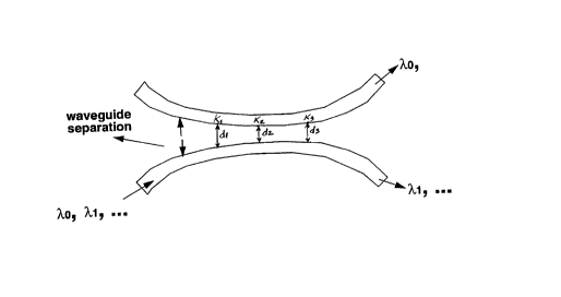
FIGURE 8 illustrates, generally, one practical
embodiment of the present invention. It is to be
understood that the spacing between waveguides must be such
~"
that the interactive strength satisfies Equation (6). This
may be achieved by curving both waveguides as shown in
FIGURE 8 or by curving only one while the second remains
straight.
It is known that the interaction strength between
the two waveguides depends exponentially on their
separation,
K = KOexp(-~) Equation (8)
where d is the separation between the two waveguides (edge
to edge). In Equation (8), Ko and r are constant
coefficients that need to be determined for a specific
device. By selecting two values of separation di and d2,
two corresponding values of coupling strength, K, and K2
may be determined by well known methods (see Haus et al,
IEEE J. Lightwave Technology, Vol. LT-5, No. 1, pp. 16-23,
1987). Hence we may solve for the coefficients of Ko and
Y-
Equation (8) may be rearranged to write d in
terms of K,
d = ~ln(K~ 4) Equation (9)
K- LC is the normalized coupling strength of
Equation (6), (that is, k(z) = K-LC). Hence the physical
separation d, given in terms of the normalized coupling
strength k(z) is
y k(ZILc) ~quation (10)
where Z is the physical distance, LC is the coupler's
interaction length, z is the normalized distance given
by Z = L ~ and k(z) = k(Z/Lc) is the function given in
Equation (6).
~ % ~ ~ ~
13
These values can then be used to plot d vs Z or
the relationship can be incorporated into mask layout
design software to generate the necessary pattern to
produce the waveguides.
The practical embodiment of the invention can be
implemented in semiconductor material such as III-V or II-
VI alloy compounds as well as a SitGe system. The
configuration is also applicable in silica, glass, polymers
and photorefractive materials such as lithium niobate.
While particular examples of the invention have
been described it will be apparent to one skilled in the
art that variations and alternatives are possible. Such
variations include both lateral and vertical coupling of
the waveguides. Also included are waveguides in which one
or both are provided with gratings 4, as shown in FIGURE 9.
It is also contemplated that the waveguides can be provided
with electrode means 6 (FIGURE 10) in order to effect
electro-optic tuning. It is to be understood, however,
that such variations and alternatives fall within the scope
of the invention as defined by the appended claims.
,,~''.