Note: Descriptions are shown in the official language in which they were submitted.
._ 2~ b8 ~ ~~
- 1 - 94-PDC-297
ELECTRICAL APPARATUS WITH WIDE DYNAMIC
RANGE FOR MONTTORING AND PROTECTING
ELECTRIC POWER SYSTF~IS
BACKGROUND OF THE llYVF.~'YTION
Field of the Invention
This invention relates to apparatus which responds to electrical signals
having a wide dynamic range, particularly the currents and voltages in an
electric
power distribution system. It also relates to such apparatus which responds to
voltages
of wide dynamic range in three-phase electrical systems without a neutral.
Back~c~ound Information
Electrical apparatus such as monitors, meters and analyzers used with
electrical power systems often must respond to signals with wide dynamic
ranges. This
is also true of circuit interrupters used in such systems which also
incorporate metering
functions as well as protection functions. Such electrical apparatus commonly
employs
ranging circuits to handle the wide dynamic ranges of the input currents and
voltages.
These ranging circuits typically utilize multiplexers to switch signals from a
resistor
ladder into the input of an operational amplifier. However, with the ranging
in the
input circuit of the operational amplifier, the maximum input voltage must be
designed
to be less than the voltage rating of the analog switches of the multiplexer.
This means
that small input voltages must be measured at the low end for signals with
wide
dynamic range, and over-voltage protection for the analog switches must be
added.
Attempts to place the multiplexer in the feedback circuit of the operational
amplifier
have produced inaccurate results because the analog switch resistances became
part of
the gain determining resistance.
n-
21~~i~~
2 ' 9-t-PDC-?97
'there is a need therefore. for improved apparatus which responds to
electrical signals of wide dynamic range.
t~iore particularly, there is a need for such improved apparatus which
does not require that the switches of the ranging circuit be able to withstand
the
maximum voltage produced by the wide dynamic range input signal.
There is a further need for such improved apparatus which can include
the multiplexer switches in the output circuit of the operational amplifier
without
generating inaccuracies in the conditioned signal.
There is a further need for such improved electrical apparatus responsive
to wide range signals in three-phase electric power systems.
There is also a need for such improved apparatus which can provide
accurate ranging for phase-to-neutral voltages in three-phase electrical
systems without
a neutral.
SUMMARY OF THE nVVENTTON
I S These and other needs are provided by the invention which is directed
to electrical apparatus for use with an electrical system having power related
waveforms with wide dynamic ranges. The improved apparatus places the
multiplexer
in the output circuit of the ranging circuit operational amplifier without
affecting the
accuracy of the conditioned signals. This is achieved by connecting the
multiplexer
directly to the output of the operational amplifier with the multiple outlets
of the
multiplexer then connecting precision resistors in a feedback loop to the
input of the
operational amplifier. The output is then taken not from the output of the
operational
amplifier, but from a point between the multiplexer and the precision
resistors so that
the multiplexer switch resistances are not part of the gain determining
resistance. The
output is taken through a second operational amplifier connected as a
follower. The
second operational amplifier should draw very little current, and therefore
can be a
device such as a bi-FET.
More specifically, a plurality of precision resistors are connected in
series. One of the resistors is connected between one of the outputs of the
multiplexer
and the inverting input of the first operational amplifier. The other
precision resistors
are each connected between adjacent outputs of the multiplexer between the
first output
and a last output. The second, buffer operational amplifier is connected as a
voltage
follower to the last output of the multiplexer. In a three-phase system,
separate
2~~8~~~
- 3 - 9.i-PDC-?97
ranging circuits are provided for each of the current and voltages to be input
to the
apparatus.
As another aspect of the invention, in a three-phase electrical system
without a neutral, an artificial neutral is created by connecting thee neutral
generating
resistors in a wye to the phase conductors. This artificial neutral is then
connected to
an inverting input of an artificial neutral operational amplifier to generate
a voltage
representing the difference between the artificial neutral voltage and ground.
This
artificial neutral voltage is then subtracted from the phase voltages applied
to the
respective ranging circuits by connecting the output of the artificial neutral
operational
amplifier to the inverting input of the first operational amplifier of each of
the voltage
ranging circuits.
BRIEF DESCRIPTION OF THE DRAWINGS
A full understanding of the invention can be gained from the following
dexription of the preferred embodiments when read 'in conjunction with the
1 S accompanying drawings in which:
Figure 1 is a schematic diagram of a monitor/waveform analyzer for an
electric power distribution system incorporating the invention.
Figure 2 is a schematic circuit diagram of the ranging circuits for
currents which form part of the monitor/waveform analyzer of Figure 1.
Figure 3 is a schematic circuit diagram of the ranging circuits for
voltages which form part of the monitor/analyzer of Figure 1.
DESCRIPTION OF THE PREFERRED EMBODIMENTS
The invention will be dexribed as applied to a monitor/analyzer used
to perform metering functions and waveform analysis in a power distribution
system.
Such apparatus must typically respond to signals having wide dynamic ranges.
Application of the invention to a monitor/analyzer is for illustrative
purposes only, and
it will be evident to those skilled in the art that the invention has
application to other
apparatus which is responsive to electrical signals with wide dynamic ranges.
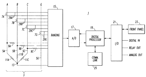
As shown in Figure 1, the exemplary monitorlanalyzer 1 to which the
invention has been applied, is used to monitor and analyze an ac electrical
power
system 3 such as a power distribution system. The power distribution system 3
illustrated has three phase conductors SA, SB and SC, and a ground conductor
SG.
The power distribution system 3 could also have a neutral conductor, although
such a
i
CA 02168159 2002-02-08
- 4 - 9.t-PDC-'_N7
conductor is not shown in the system of Figure 1 in order to illustrate an
aspect of the
invention applicable to systems without a neutral conductor.
Current transformers 7A, 7B, 7C and 7G sense current tlowing in the
respective conductors while phase-to-ground voltages are sensed through
sensing
resistors 9A, 9B and 9C. An artificial neutral is generated in accordance with
the
invention by three neutral generating resistors t lA, llB, and l 1C connected
in a wye
between the respective phase conductors SA, SB, and SC and a neutral node ! 3.
The sensed curnent signals generated by the current transformers 7A, 7B.
and 7C, the sensed phase to ground voltages generated by the resistors 9A, 9B.
and 9C
and the artificial neutral voltage generated at the node 13 are applied to a
ranging
circuit 15 which, as will be described, converts the range of the signals for
application
to an analog to digital (A/D) converter 17 for input to a digital processor
19. The AID
converter l7 samples the analog voltages and currents at sampling rates
determined by
interrupts generated by the digital processor 19.
The digital processor 19 utilizes the data generated by the digital samples
to perform the metering and analyzing functions. The metering function
includes the
calculation of parameters such as rms curnents and voltages, peak currents and
voltages, minimum currents and voltages, power factor, watts, Vars, volt-amps,
K-
factor, CBMEA Berating factor, and the like. For the analysis function, the
monitor/analyzer 1 stores the raw waveform data for later or remote display,
arid
calculates therefrom harmonic distortion. The digital processor 19 has an
input/output
(I/O) 21 through which the processor 19 is connected to a front panel 23. The
front
panel 23 serves as the interface with the user. It is through the front panel
23 that the
user can control operation of the monitorlanalyzer 1 and monitor the ac
electrical
power system 3. The I/O device 21 also interfaces the digital processor 19
with
contact inputs through a digital input. Relay outputs and analog outputs are
also
provided through the IIO device 21. The digital processor 19 can also
communicate
with a remote processor through a communications link 25. Through this
communications link 25, the monitor/analyzer 1 can provide information to
andfor be
controlled by a remote processor (not shown).
Figure 2 illustrates the circuits within the ranging circuit 15 which
selectively apply appropriate gain to the sensed current signals generated by
the current
transformer 7 for conversion by the AID converter module 17. Each of the
current
I
CA 02168159 2002-02-08
- 5 - y-4-PDC-297
ranging circuits 27A, 27B. 27C and 27G has an input lead 29A. 29B. 29C and 29G
connected through a connector 3l to one side of the secondary winding of the
corresponding current transformer 7A, 7B, 7C and 7G. The other side of the
secondary winding of each of the current transformers is connected through the
connector 31 to analog ground. The ranging circuits 27 for all of the phase
currents
are identical, hence only the circuit for phase A will be described. The
current from
the secondary current transformer is converted to a voltage by a resistor 33.
'This
voltage is applied to the inverting input of a first operational amplifier 35
through an
input resistor 37. The non-inverting input of the operational amplifier 35 is
connected
to analog ground. A feed back loop 39 connected from the output to the
inverting
input of the operational amplifier 35 includes a plurality of precision
resistors 41, 43
and 45 connected in series. A multiplexer 47 comprises a plurality of solid
state
switches 49, 51 and 53 each having one terminal connected to a common terminal
on
the other switches to form a common input 55 which is connected to the output
of the
first operational amplifier 35. The other terminal of the switch 49 forms the
fu-st
multiplexer output 57 which is connected between the precision resistors 41
and 43.
The second terminal of the switch 51 is connected between the resistors 43 and
45 to
form a second output 59 of the multiplexer, while the second terminal of the
switch 53
forms the last output 61 of the multiplexer which is connected to the
precision resistor
45.
It can be seen then that the gain applied by the first operational amplifier
35 to the input signal is a function of the ratio of the total resistance of
the resistors 41,
43 and 45 inserted in the feedback loop by the multiplexes 47 to the value of
the
resistance of the input resistor 37. In the exemplary embodiment of the
invention, the
values of the resistors 37, 41, 43, and 45 are selected such that the gain of
the
operational amplifier 35 is 1:4:8 with the switches 49, 51 and 53 closed
respectively.
The input of a second operational amplifier 63 is connected as a voltage
follower to the last output 61 of the multiplexes 47. With this arrangement,
the
resistance of the selected switch of the multiplexes 47 is not part of the
gain determining
resistance which sets the magnitude of the voltage seen by the follower op amp
63.
However, this second operational amplifier 63 must have a high input impedance
so
that negligible current is drawn through the resistor 45 when the switch 51 is
closed
or through the resistors 43 and 45 when the switch 49 is closed. In the
exemplary
2168159
- 6 - 9-t-PDC-297
embodiment of the invention a bi FET is used for the operational amplifier 63
to satisfy
this requirement. Noise suppressing capacitors 65 are provided across the
feedback
resistors 41, 43 and 45.
As mentioned, the current ranging circuits 27B, and 27C for the other
phase currents (and for the neutral current if a neutral conductor were
present) are
identical to that just described for phase A. A ranging circuit is not
required for the
ground current, as this signal remains within a range which can be
accommodated by
a single gain setting. Thus, the ground current signal is converted to a
voltage by the
resistor 67 and applied through an input resistor 69 to an operational
amplifier 71. A
single precision resistor 73 is provided in a feedback loop. A capacitor 75
across the
feedback resistor 73 suppresses high frequency noise.
As discussed in connection with Figure 1, the outputs of the current
ranging circuits are applied to the A/D converter 17. In the exemplary
implementation
of the invention, AOD7874BR A/D converters 17a and 17b are utilized. Each of
these
IS A/D converters incorporates a four input multiplexer. Thus, the conditioned
currents
from the current ranging circuits 27A, 27B, and 27C are applied to the AID
converter
17a while the ground current is applied to the A/D converter 17b. These A/D
converters 17a and 17b convert the applied analog signal into twelve bit
digital signals
for input to the digital processor on data lines 77. Selection of the analog
signal to be
converted is controlled by the digital processor 19.
Figure 3 illustrates the voltage arranging circuits 81A, 81B and 81C for
the respective phase voltages. Again, only the ranging circuit 81 A for the
phase A
voltage will be explained in detail. The phase A voltage ranging circuit 81 A
is
connected to the sensing resistor 9A thmugh a connector 83 and input lead 85A.
The
sensed voltage is applied to the inverting input of a first operational
amplifier 87 which
is referenced to ground through its non-inverting input. As in the case of a
current
ranging circuit, a feedback loop 89 for the op amps 87 includes a plurality of
precision
resistors 91, 93 and 95 connected in series, and a multiplexer 97 which
includes a
plurality of switches 99, 101 and 103. One terminal of each of the switches
99, 101
and 103 is connected to a common terminal on the others to form a multiplexer
input
105. The second terminal of the switch 99 forms a first output 107 of the
multiplexer
97 which is connected between the precision resistors 91 and 93. The second
output
of the switch 101 forms the second output 109 of the multiplexer 97 connected
between
2i 68i 5~
- 7 - 9-t-PDC-?97
resistors 93 and 95. while the second output of the switch l03 forms a last
output 1 1 l
of the multiplexer 97 which is connected to the resistor 95. Again, the ratio
of the
total resistance of the selected precision resistors 91, 93 and 95 to the
resistance of the
sensing resistor 9A determine the gain of the op amp 87. As in the case of the
current
ranging circuits, the values of these resistors are selected such that the
ratio of the
gains with the switches 99, 101 and 103 closed are 1:2:4, respectively. The
capacitors
113 suppress noise across the precision resistors 91, 93 and 95.
A second operational amplifier 115 is connected to the last output 1 l 1
of the multiplexer 97 as a voltage follower to generate the output for the
ranging circuit
81. As this voltage ranging circuit is similar to the current ranging circuit
described
above, the resistances of the switches 99, 101, and 103 are not part of the
feedback
resistance which determines the gain of the op amp 87, and thus, do not
produce an
error in the conditioned signals. The second operational amplifier 115 is also
a bi FET
amplifier which draws negligible input current so that the resistors 93 and 95
do not
cause any appreciable error in the output signal.
If as in the exemplary power system there is no neutral conductor, so
that the artificial neutral 13 is formed as d.ixussed in connection with
Figure 1,
circuitry is provided in Figure 3 for generating an artificial neutral to
ground voltage
which is subtracted from the voltage sensed by the sensing resistors 9 to
provide that
the voltage output by the second operational amplifier 115 is a phase to
ground voltage.
In the exemplary embodiment of the invention, the artificial ground 13 is
formed by
bringing the leads from the neutral forming resistors 11A, 11B and 11C in
through the
connector 83. The voltage of this artificial neutral is applied to the
inverting input of
an operational amplifier 119. The non-inverting input of the op amp 119 is
connected
to analog ground so that the output of the operational amplifier 119 is the
artificial
neutral to gmund voltage. The value of the feedback resistor 121 for the
operational
amplifier 119 is selected to provide a gain of 1. A capacitor 123 suppresses
noise in
the feedback circuit. As the neutral to ground voltage is inverted by the
operational
amplifier 119 it can be subtracted from the phase-to-ground voltage sensed by
the
resistor 9A by connecting it through a resistor 125 to the inverting input of
the op amp
87. A switch 127 allows the neutral to ground voltage to be applied to the
operational
amplifier 87 only when a neutral conductor is not present. With a neutral
conductor
2~ f~81 ~9
- 8 - 9a-PDC-297
provided the phase to neutral voltage is available directly by connecting the
primary
of a potential transformer between the phase conductor and the neutral
conductor.
The ranging circuits 8lB and 81C for the phase B and C voltages
respectively are similar to the circuit 81A. These conditioned voltage signals
are
applied to the second A/D converter chip 176 for selection for digital
conversion for
input for the digital processor 19.
While specific embodiments of the invention have been described in detail, it
will be appreciated by those skilled in the art that various modifications and
alternatives
to those details could be developed in Gght of the overall teachings of the
disclosure.
Accordingly, the particular arrangements disclosed are meant to be
illustrative only and
not limiting as to the scope of invention which is to be given the firll
breadth of the
claims appended and any and all equivalents thereof.