Note: Descriptions are shown in the official language in which they were submitted.
~ 0 95/05023 2 1 6 8 3 ~ 9 PCT/US94/08751
METHOD AND APPARATUS FOR RMS CURRENT APPROXIMATION
Description
Technic~l Field
Applicant's invention relates generally to the conversion
and measurement of the current of an electrical load, and more
particularly to an apparatus that will produce a signal
proportional to the rms current of the load.
1 0
Rack~round Art
Many methods have been utilized to measure the AC current
flowing to a load. These methods are used as part of more
complex devices such as solid state breakers or overload relays,
AC line monitoring devices, or current feedback control loops as
required for motor drives and power supplies. The application
usually determines the degree of measurement accuracy required.
Root-mean-square (rms) current is generally considered to be an
accurate representation of the actual current flowing in the
circuit being monitored. For simple systems, this may not be
necessary and instead, average current over a set time period,
usually one cycle, is used to represent the actual current. Other
systems will use peak current over the same time period as the
basis. More sophisticated microprocessor based devices will
actually compute the rms value by sampling the current
waveforms many times during each time period, and using those
sample measurements to generate the value of the current over
the time period.
Using a solid state overload relay as an example of one such
application, a common method used to generate a signal
representative of the line current is to use a peak detecting
circuit as disclosed in commonly assigned U.S. Patent 4,345,288.
r Although this device provides a close approximation of a
standard thermal electromechanical overload unit, the device
35 does not compensate for non-sinusoidal currents that may be
encountered in some instances. Likewise, line harmonics and
transients may cause erroneous results. A microprocessor based
CA 021683~9 1998-01-1~
device to accomplish a similar function is outlined in U.S. Patent 5,220,478 which will
compute the rms current through digital sampling techniques. Whereas this is a more
accurate method, it is a relatively expensive solution because of the increased component
requirements for support circuitry and the increase in the size of the device to house the
extra components. For a low cost application where size is also a factor, it would be
desirable to provide a solid state overload relay that computes an approximation of the
rms current without the complexity of a microprocessor based device.
Summary of the Invention
Accordingly, the principal object of the present invention is to provide a method
and apparatus for the conversion of the current of a polyphase electrical load to a signal
proportional to the RMS current of the load.
A further objective of the invention is to provide an overload relay function
employing the method and apparatus of current conversion of the present invention.
Another objective of the invention is to provide a method and apparatus for
monitoring the current of a load by providing a signal proportional to the rms current of
the load.
The invention may be employed to provide a method and apparatus for providing a
current feedback signal of a load proportional to the rms current of the load.
In accordance with one aspect of the present invention, there is provided a method
of approxim~ting the rms current of a load supplied power from an AC source
comprising: a. sensing actual current supplied to said load from said AC source; b.
converting said actual current to a first voltage proportional to said actual current; c.
generating a second voltage equivalent to an average value of said first voltage; d.
generating a third voltage equivalent to a peak value of said first voltage; and e.
sl~mming a fraction of said second voltage with a fraction of said third voltage to provide
said output signal proportional to the rms current supplied to said load from said source.
In accordance with another aspect of the present invention, there is provided anapparatus for approxim~ting the rms current of a load supplied power from an AC source
comprising: a. means to sense actual current supplied to said load from said AC source;
~ CA 021683~9 1998-01-1~
b. means to convert said actual current to a voltage proportional to said actual current; c.
means to generate a first voltage from said proportional voltage equivalent to an average
value of said voltage; d. means to generate a second voltage from said proportional
voltage equivalent to a peak value of said voltage; and e. means to sum a fraction of said
first voltage with a fraction of said second voltage to provide said output signal
proportional to the rms current of said load.
In accordance with yet another aspect of the present invention, there is provided a
solid state overload protective apparatus for an AC load supplied power from an AC
source comprising: a. means to sense actual current supplied to said load from said AC
source; b. means to convert said actual current to a first voltage proportional to said
actual current; c. means to generate a second voltage from said first voltage, said second
voltage proportional to an approximate value equal to the rms current of said load; d.
means for integrating said second voltage to provide a trip signal representative of a
predetermined full load carrying capacity of said AC load; e. means for comparing said
trip signal with a predetermined trip reference voltage level, said comparator means
producing a drive output signal when said trip signal is a lessor m:~gnit~lde than said trip
reference voltage level, and said comparator means producing a turn-off drive output
signal when said trip signal is a greater m~gnit~lde than said trip reference voltage level
indicative of an overload condition; and f. means for removing said AC source from said
load responsive to said drive output signal when said overload condition exists.In accordance with yet another aspect of the present invention, there is provided
an apparatus for approxim~ting the rms current of a load supplied power from an AC
source comprising: a. means to sense actual current supplied to said load from said AC
source; b. means to convert said actual current to a first voltage proportional to said
actual current; c. means to generate a second voltage from said first voltage, said second
voltage proportional to an approximate value equal to the rms current of said load; and d.
wherein said second voltage generating means includes an approximation circuit, said
approximation circuit having first means to generate a voltage from said first voltage
proportionally equivalent to an average value of said actual current, second means to
generate a voltage from said first voltage proportionally equivalent to a peak value of said
actual current, and third means to sum a fraction of said voltage from said first means
~ CA 021683~9 1998-01-1~
3a
with a fraction of said voltage from said second means to provide said second voltage
proportional to the rms current of said load.
In the preferred embodiment of the invention, conventional current transformers
sense the current flow in each phase of the load. The load typically could be a single or
three phase motor. The current transformers generate an output current signal that is
proportional in magnitude to the sensed current. This output is coupled to a current to
voltage converter circuit to create a voltage that is also proportional in m~gnitll(le to the
sensed current. This voltage signal is applied to two circuits connected in parallel, one to
measure the peak value of the voltage and the other to measure the average value of the
voltage over one cycle of the applied AC voltage. The outputs of both of these circuits
are connected together at a sllmming junction through different valued resistors of a
buffer amplifier. These different resistance values at the input to the sllmming point
serve as to provide different weighting factors to the two signals to produce a composite
voltage signal. This signal will be a DC level, which for a sinusoidal current, closely
approximates a scaled rms value of the original input load current. For the common non-
sinusoidal current waveforms encountered in most applications, this circuit will retain its
accuracy to within a +/- 5% of the true rms value.
For a current monitoring function, this output can preferably be converted and
scaled to a digital representation of the load current and visually displayed. To provide
an overload or circuit breaker function, this output is fed to a time integrating circuit to
produce various trip curves, the output of which is compared with a predetermined trip
reference voltage signal. When this output exceeds this level, the overload or breaker
will trip, providing an output contact or contacts that will change state when this does
occur.
Various power conversion devices such as PWM inverters require a current
feedback signal representative of the load current as a controlling element of the device
for current limit control. The output voltage of the present invention can provide this
function by lltili7ing this output, with proper scaling factors, as an input to the inverter as
the current feedback signal which is proportional to the rms current of the load.
Other features and advantages of the invention, which are believed to be novel and
non-obvious, will be apparent from the following specification taken in conjunction with
the accompanying drawings in which there is shown a preferred embodiment of the
CA 02168359 1998-01-15
- 3b -
invention. Reference is made to the claims for hltel~leLillg the full scope of the invention
which fs a~l nw~a~nly apla~ l bv ~ h a~bu~
WO 95/05023 ~ 1 6 8 3 5 9 }'CT/US94/08751
Brief Description of Drawings
FIG. 1 is a diagram of a typical prior art solid state
overload relay (SSOLR).
FIG. 2 is a schematic block diagram of a SSOLR utilizing a
system for converting the load current to an approximation of the
rms value of the current according to the present invention.
FIG. 3 is a detailed schematic block diagram of the
approximation circuit as depicted in Fig. 2.
FIG. 4 is a block diagram of a current monitoring device
utilizing the system for converting the load current to an
approximation of the rms value of the current according to the
present invention.
FIG. 5 is a block diagram of a current controlled inverter
with a current feedback loop utilizing the system for converting
the load current to an approximation of the rms value of the
current according to the present invention.
Detailed Description
Although this invention is susceptible to embodiments of
2 0 many different forms, a preferred embodiment will be described
and illustrated in detail herein. The present disclosure
exemplifies the principles of the invention and is not to be
considered a limit to the broader aspects of the invention to the
particular embodiment as described.
FIG. 1 illustrates a typical solid state overload relay
protective device 1 representative of prior art. A circuit breaker
function would be similar. Three phase incoming power L1-L3 is
fed to a load 2. The load could be lighting equipment, heating
equipment or inductive loads such as motors, magnets, brakes or
coils. Current sensors 4 monitor the load currents 11-13 to
create currents i1-i3 respectively which are proportional in
magnitude to the sensed currents. The current sensors 4
generally are current transformers. A current to voltage
converter 6 transforms the three currents i1-i3 to an output
voltage Vo that is proportional to a composite of the sum of the
three currents. The resulting voltage Vo is mostly DC with about
~wo gs/0so~3 2 1 6 8 3 5 9 ~CT/USg4l08751
a 10% ripple for balanced sinusoidal currents. A peak detecting
circuit 8, typically consisting of a diode and a capacitor, will
capture the peaks of the ripple voltage Vo to generate a voltage
V1 which will be a DC voltage that is proportional to the peak
5 current of the load 2. The overload relay function is time based
and not instantaneous. The greater the magnitude of the
overload, the faster the overload relay must trip out. Therefore,
time integrator amplifier 10 will integrate voltage V1 to create
~ a voltage V2 which has an inverse time relationship with the
10 magnitude of the sensed currents 11-13. Voltage V2 is an
exponential response to the input voltage V1. When an overload
condition arises, V2 will start ramping up above a level that
represents the 100% current rating of the overload relay. To
create the overload trip curve, a voltage 12, as set by trip level
15 setting circuit 14 is computed such that the output of the time
integrator amplifier 10 will reach this voltage level 12 if the
overload condition exists for a predetermined amount of time.
For instance, if the overload condition is at 600% of the rated
load, this time might be set at 10 seconds and be set at 200
20 seconds if the overload is at 200% of the load. Trip level
comparator 16 will compare voltage V2 with this predetermined
voltage 14 and will output a signal 18 that will energize control
relay 22 through output amplifier 20 once voltage V2 exceeds set
level voltage 14. Comparator 16 will function as a schmidt
25 trigger in that once this comparison has been exceeded, the
output 18 will remain in the tripped state until output V2 has
decayed below a second predetermined reset level 24 and the
reset 26 is activated, either manually or automatically.
Contacts 28 from relay 22 are used to disconnect the power
30 L1-L3 from the load, the details of which are well known, when
the overload relay has tripped.
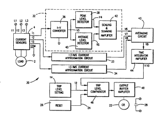
Referring to Fig. 2, an improved solid state overload
relay 30 is detailed utilizing a system for converting the load
currents L1-L3 to an approximation of the rms value of the
35 current according to the present invention. Although a three
phase system is disclosed, it is to be understood that a single
WO ~15/05073 2 1 6 ~3 ~9 PCT/Us94l087s1
phase or polyphase system would function in a similar manner.
As discussed above, three phase incoming power L1-L3 is fed to a
load 2. Current sensors 4 monitor the load currents 11-13 to
create the proportional currents i1-i3, respectively. Each of the
currents i1-i3 is independently processed by an rms current
approximation circuit 32-34, the object of the present invention.
Current i1 is converted to a voltage V3 by an l-V converter 36.
V3, which is proportional to the load current 11, is divided into
two paths, one to a peak level detecting circuit 38 and the other
to an average level measuring circuit 40. Peak level detecting
circuit 38 will capture the peaks of the ripple voltage V3,
generating a voltage level V4. Average level measuring circuit
40 generates a voltage V5 which will be a DC voltage that is
proportional to the average current of the load 2. V4 and V5 are
inputted to scaling and summing amplifier 42 which generates a
voltage V6 which is a proportional rms approximation of the
sensed line current 11.
It has been empirically determined that an accurate
approximation of the line current can be attained based on the
20 equation:
Irms = 0.22~1pk + 0.766~1ave
where: IrmS is the root mean square current,
Ipk is the peak value of current, and
lave is the average value of current.
Scaling and summing amplifier 42 solves this equation to create
the DC output voltage V6 which is proportional to rms value of
the line currents L1-L3. For most non-sinusoidal currents, a +/-
30 5% accuracy for the approximation can be attained. Thiscompares with a 30% accuracy common for traditional systems
based on a peak detecting method.
Likewise, rms current approximation circuits 33 and 34,
which are identical with circuit 32, will generate output
35 voltages V7 and V8. The output voltages V6-V8 are fed to an
averaging circuit 43 which will combine them to create a
WO 95/05023 2 ~ 6 8 3 ~ q PCT/US94/087~1
composite DC voltage V9 which is proportional to the average of
the three rms phase currents 11, 12 and 13. V9 is inputted to time
integrator circuit 44 which, along with the trip level comparator
46, and output buffer amplifier 48 provides the timing function
5 and output relay contacts as previously discussed for the
overload relay function and is identical with the system
disclosed above. For a single phase system, only rms current
approximation circuit 32 is required and output voltage V6 is fed
directly to the time integrator circuit 44.
For the preferred embodiment of the present invention,
Fig. 3 details the approximation circuit 32 as depicted in Fig. 2
which comprises the current to voltage converter 36, the peak
level detecting circuit 38, the average level measuring
circuit40, and the scaling and summing ampiifier 42. As
15 previously mentioned, approximation circuits 33-34 are identical
to circuit 32. Load currents L1-L3 are monitored by current
transformers in each of the three phase conductors. The
secondaries of the current transformers produce currents i1, i2,
and i3. Currents i1-i3 are reduced in magnitude based on the
20 turns ratio of the current transformers. Each phase current is
measured separately by the current to voltage converter circuit
36 in each of the approximation circuits 32-34. Bridge rectifier
BR1 produces a full wave rectified current from i1 to generate a
full wave rectified voltage V3 across burden resistor R1.
25 Voltage V3 is divided into two paths, one to peak level detecting
circuit 38 through resistor R2 and the other to average ievel
measuring circuit 40 through resistor R3.
The peak detecting circuit 38 consists of a first op amp
IC1A, which together with diode D1 combine to form an ideal
30 diode combination and capacitor C2. The ideal diode combination
eliminates a voltage drop normally associated with a standard
diode which would result in errors in the output voltage V4.
Resistor R4 connected in parallel with C2 provides a discharge
- path with a long time constant to avoid the circuit from
35 becoming just a sample and hold circuit. C2 has low resistance
in its charging path and high resistance in its discharge path so
wo ss/nso23 2 1 6 8 3 ~ q PCT/U59~/08751
that the voltage across C2 will essentially be proportionally
equal to the peak value of the input voltage V3. Op amp IC1B
provides a buffer for output V4 to avoid the input impedance of
the next stage from causing an error in the C2 voltage. The
output V4 of buffer amp IC1B thus represents this peak voltage.
A series connected resistor R3 and capacitor C1 combine to
form the average level measuring circuit 40. The voltage across
C1 will be proportional to the average of the voltage V3. R3 and
C1 are scaled to provide this function over the frequency range
from 48 Hz to at least 780 Hz. Op amp IC1C provides a buffer for
output V5 to avoid the input impedance of the next stage from
causing an error in the C1 voltage. The output V5 of buffer amp
IC1C thus represents the average of the V3 voltage.
Scaling and summing amplifier circuit 42 receives voltages
V4 and V5 at a summing junction of op amp IC1D through
resistors R6 and R5 respectively. The values of these resistors
along with feedback resistor R7 are calculated such that the
output V6 of the summer amplifier IC1 D will be proportional to
fractions of the each input V4, V5, so as to solve the equation
IrmS = 0.22~1pk + 0.766*laVe. Output voltage V6 is a DC voltage
which has been empirically determined to be proportional to the
rms value of the line currents L1-L3 for sinusoidal currents and
having, for most non-sinusoidal currents, an accuracy that is
within 5% of the true rms value. For a single phase system,
voltage V6 can be directly coupled to time integrator amplifier
44 as disclosed in Fig. 2 to create the improved solid state
overload relay previously discussed. For a three phase system,
voltage V6 is coupled to the averaging circuit 33 where it is
combined with the equivalent voltages V7 and V8 generated by
the other two phases to generate the output voltage V9 which is
proportional to the average of the three rms phase currents
11-13. The op amp circuits IC1A-D are supplied from a dual rail
+/- 12VDC power supply, not shown, but the details of which are
well known.
3 5 FIG. 4 illustrates a current monitoring device 100 utilizing
the rms approximation circuits 32-34. The load currents L1-L3,
WO 95/05023 PCT/US94/08751
~ 1 6835~
as before are sensed by current sensors 4 to generate proportion
currents i1-i3. The approximation circuits 32-34 will generate
voltages V6-V8, as before, for inputting to a buffer amplifier
102 which will in turn drive a display 104 for a visual indication
5 of the rms value of the line currents, either individually or an
rms average of the three phase currents. Instead of displaying
these currents, buffer amplifier 102 could also input this
information to a communications network or other devices
whereby information of the line currents is desired.
Another use of the rms approximation circuit 32 is
depicted in FIG. 5. Current controlled inverters require a current
feedback signal to either limit output currents and other control
functions. An AC/DC converter will create a DC bus 122 which
provides the source of the three phase output voltages. Since the
15 output voltages are pulse width modulated by PWM inverter 124,
the output voltages are not sinusodial and the approximation
circuit 32 provides a means for converting the load currents to
an approximation of the rms value of the current. Although a
single phase current signal is shown, three phase monitoring
2 0 could be used with the addition of rms approximation circuits 32
in the other two phases for controlling the PWM inverter 124.
While the specific embodiments have been illustrated and
described, numerous modifications are possible without
departing from the scope or spirit of the invention. Although in
25 the foregoing embodiments have been applied to single and three
phase systems, it will be clearly understood that the invention is
equally applicable to polyphase systems, with the requirement
being the addition or subtraction of a separate rms
approximation circuit for each phase of the voltage source,
3 0 adjustments in the time constants of the resistor-capacitor
combinations in the peak level detecting and average level
detecting circuits, and changes in the averaging circuit that
combines the outputs of the rms approximation circuits.