Note: Descriptions are shown in the official language in which they were submitted.
CA 02168859 2006-07-26
78807-1
-1-
FLUID DOSE, FLOW AND COAGULATION SENSOR FOR MEDICAL
INSTRUMENT
Technical Field
This is a related application to U.S. Patent
No. 5,832,921, titled ANALOG HEATER CONTROL FOR MEDICAL
I:L~STRUMENT, U.S. Patent No. 5,792,944, titled POWER SUPPLY
MONITOR AND CONTROL FOR MEDICAL INSTRUMENT, U.S. Patent
No. 5,849,023, titled MAGNETIC SYSTEM FOR MEDICAL
INSTRUMENT, WO 95/06868, titled REAGENT AND METHOD OF ITS
USE, and U.S. Patent No. 5,526,111, titled METHOD AND
APPARATUS FOR OPERATING A MEDICAL INSTRUMENT, all filed on
the same date as this application and assigned to the same
assignee.
This invention relates to method and apparatus for
determining blood coagulation times.
Background Art
Several methods are known for determining blood
coagulation time. These include laser speckle methods,
ultrasonic measurement methods, transmission direct clotting
methods, ball and tilted cup direct clotting methods, and
the methods illustrated in, for example, U.S. Patents:
4,756,884; 4,849,340; 4,963,498; 5,110,727; and, 5,140,161.
Many of these prior art methods do not measure blood
coagulation times directly, and thus are subject to errors
that can enter into indirect measurement processes. Many of
these methods do not determine whether there is an adequate
blood sample, and thus are subject to errors that can enter
into processes which do not determine adequacy of the blood
sample. Many of these methods do not distinguish between
blood and control or test solutions, and thus are subject to
errors that can enter into processes which do not determine
CA 02168859 2006-07-26
78807-1
-2a-
whether a specimen being tested is blood or a control or
test solution. Many of these methods do not accurately
ascertain the start of a coagulation test, and
WO 95/07452 PCT/US94109505
2168859
-2-
thus are subject to errors that can enter into processes
which do not ascertain accurately the start of a
coagulation test. None of these methods combine the
specimen heating function required to obtain accurate
coagulation time test results with a radiation reflector
for reflecting test parameters to a radiation detector.
Disclosure of Invention
According to the invention, a system is provided
for determining coagulation time directly by a reflectance
technique. According to an illustrative embodiment of the
invention, a coagulation testing meter employs a
combination of reflectance sensors and a sample
application, start, fill and assay technique to determine
coagulation time.
An easy-access, cleanable adapter can be opened
by pushing a release button located on the front of the
instrument. This provides for easy cleaning in the event
that contamination occurs during the conduct of a test.
The adapter top is hinged toward the back of the adapter
and pops up in somewhat the same manner as a car hood when
the release button is actuated. The adapter top has a flag
that blocks a light path of an interrupt sensor to indicate
when the top is closed in testing position.
A combination reagent heater and reflector
includes an aluminum nitride heater plate which heats the
reagent test strip to a controlled temperature and acts as
an optical reflector for a start sensor, an adequate sample
sensor, and an assay sensor. A sample sensor which reads
through the clear bottom of a coagulation time test strip
dictates the need for a heater plate that reflects light.
A sample application icon is a yellow dot that is
viewed by the user through the clear bottom of the test
str~.p to indicate to the user where to apply the sample,
the coagulation time of which is to be determined.
WO 95/07452
216 ~ 8 5 9 pCT~S94/09505
-3-
A sample flow sensor detects that adequate sample
has been applied to the test strip and identifies the type
of sample, that is, control or blood, by the flow time
signature. The flow time is calculated as the time
difference between actuation of a flow sensor and actuation
of a start sensor. This marks the sample type in the
coagulation testing instrument's memory as a control test
or a blood test. If the sample takes longer than an
established time stored in read-only memory in the
instrument to flow from the flow sensor to the start
sensor, the instrument stores an indication that the sample
volume is insufficient. The flow sensor is a reflective
sensor that senses a composite net loss in signal as a
result of change of index of refraction, scattering, and
absorption differences between air (no sample applied) and
sample (blood or control).
The start sensor detects when a sample enters the
area of a test strip coated with a coagulation time
measurement-assisting reagent. This activates a timer for
timing the clotting process. The start sensor also is a
reflective optical sensor that senses a composite net loss
in signal as a result of change in index of refraction,
scattering, and absorption differences between air and
sample. An LED light source directs light through a clear
strip to a heater plate, which reflects light back through
the strip onto a photodetector.
An adequate sample sensor is only activated if a
blood sample is detected within the established time stored
in the read-only memory. The adequate sample sensor
detects if the reagent area is covered by the sample. It
also prevents the instrument from performing the test if
the user applies a second dose of sample to the strip
(double-dosing the strip), if the second dose is applied
more than the established time after the first. The sample
must flow from the start sensor through a fill optical read
WO 95/07452 PCT/US94/09505
~~ 6859
-4-
area of the instrument within the established time, or the
instrument reports insufficient sample. The adequate
sample sensor also is a reflective sensor that senses a
composite net loss in signal as a result of change in index
of refraction, scattering, and absorption differences
between air and sample. An LED light source directs light
through the clear strip to the heater plate, which reflects
light back through the strip onto a photodetector.
An assay sensor outputs a signal that is
proportional to the change in heater plate reflectance when
modulated by spatial iron particle movement induced by a
2Hz alternating electromagnetic field. An LED light source
directs light through the clear strip to the heater plate,
which reflects light back through the strip onto a
photodetector. When the sample clots, the iron particles
are restricted from moving. The change in the reflected
light signal decreases. Data collection continues for a
predetermined period of time stored in read-only memory.
At the end of this predetermined period of time, the
collected data is analyzed to determine the clotting time.
According to one aspect of the invention, an
instrument for determining the coagulation time of blood, a
blood fraction or a control comprises a radiation-
reflective surface, a first source for irradiating the
surface, and a first detector for detecting radiation
reflected from the surface. A cuvette holds a sample of
the blood, blood fraction or control the coagulation time
of which is to be determined. The cuvette has two opposed
walls substantially transparent to the source radiation and
reflected radiation. The first source and first detector
are disposed adjacent a first one of said two opposed walls
and the radiation reflective surface is disposed adjacent a
second of said two opposed walls.
According to another aspect of the invention, a
method for determining the coagulation time of blood, a
WO 95/07452
PCTlUS94/09505
-5-
blood fraction or a control comprises irradiating a
radiation-reflective surface through a cuvette for holding
a sample of the blood, blood fraction or control the
coagulation time of which is to be determined using a first
radiation source, and detecting radiation reflected from
the surface using a first radiation detector. The cuvette
has two opposed walls substantially transparent to the
source radiation and reflected radiation.
Illustratively, according to the invention, the
instrument further comprises a second source for
irradiating the cuvette and a second detector for detecting
when a sample has been applied to a sample application
point in the cuvette. The second detector detects
radiation from the second radiation source transmitted
through one of said two opposed walls of the cuvette,
reflected by the sample and transmitted back through said
one wall to the second detector.
Additionally, illustratively according to the
invention, a third source irradiates the surface. The
first detector detects radiation from the third source
reflected from the surface. The third source is positioned
to transmit radiation through said two apposed walls for
reflection by the surface and transmission back through
said two opposed walls to the first detector to indicate
that a sample has reached a first point in the cuvette.
Further, illustratively according to the
invention, a fourth source irradiates the surface. The
first detector detects radiation from the fourth source
reflected from the surface. The fourth source is
positioned to transmit radiation through said two opposed
walls for reflection by the surface and transmission back
through said two opposed walls to the first detector to
indicate that a sample has reached a second point in the
cuvette.
WO 95/07452 ~' PCT/US94/09505
-6-
Illustratively, according to the invention, the
second point is downstream in the spread of the sample from
the first point and the first point is downstream in the
spread of the sample from the sample application point.
Additionally, according to the present invention,
a heater is provided for maintaining the blood, blood
fraction or control at a desired temperature. Means are
provided for mounting the heater adjacent the surface.
Means are provided to power the heater. Means are provided
for monitoring the surface temperature and for feeding the
monitored temperature back to the means for providing power
to the heater.
Illustratively, the heater comprises an
electrically resistive foil. The surface comprises a first
radiation reflective surface of a plate. The plate further
comprises a second surface opposite the first surface
thereof. Means are provided for mounting the electrically
resistive foil to the second surface of the plate.
Further, illustratively according to the
invention, the instrument determines coagulation time by
combining fluid blood, blood fraction or control with
particles which are affected by a magnetic field so that
the particles become suspended relatively freely in the
fluid. The instrument further comprises means for
generating a time-varying magnetic field for causing the
particles to be reoriented as the magnetic field varies,
with the reorientation changing as the fluid coagulates
owing to the fluid's changing viscosity. Means are
provided for mounting the means for generating the time-
varying magnetic field adjacent the surface.
Illustratively, the cuvette comprises a region
for bearing a code. The instrument further comprises one
or more fifth radiation sources for irradiating the code
bearing region, and one or more third detectors for
detecting the transmission of radiation through the code
CA 02168859 2006-07-26
78807-1
_7_
bearing region. The fifth radiation source or sources and
third detector or detectors are mounted adjacent the code
bearing region to detect the code.
Further, illustratively, there are multiple fifth
radiation sources and a single third detector. The third
detector has an active region which extends adjacent the
code bearing region to detect the transmission of radiation
from all of said fifth radiation sources. Means are
provided for activating the fifth radiation sources in a
predetermined sequence to permit the detection and
determination of the code borne by the code bearing region.
According to another aspect of the invention,
there is provided in combination, an instrument for
determining a coagulation characteristic of blood, a blood
fraction or a control comprising a radiation-reflective
surface, a first source for irradiating the surface, and a
first detector for detecting radiation reflected from the
surface, a heater comprising an electrically resistive foil
for maintaining the blood, blood fraction or control at a
desired temperature, means for mounting the heater adjacent
the surface, means for providing power to the heater and
means for monitoring the surface temperature and for feeding
the monitored temperature back to the means for providing
power to the heater, the surface comprising a first
r<zdiation reflective surface of a heater plate, the heater
p=late further comprising a second surface opposite the first
surface thereof, and means for mounting the electrically
resistive foil to the second surface of the heater plate,
and a cuvette for holding a sample of the blood, blood
fraction or control the coagulation characteristic of which
is to be determined, the cuvette having two opposed walls
substantially transparent to the source radiation and
CA 02168859 2006-07-26
78807-1
-7a-
reflected radiation, the first source and first detector
being disposed adjacent a first one of said two opposed
walls and the radiation reflective surface being disposed
adjacent a second of said two opposed walls.
Brief Description of Drawings
The invention may best be understood by referring
to the following description and accompanying drawings which
illustrate the invention. In the drawings:
Fig. 1 illustrates an exploded perspective view of
an instrument constructed according to the present
invention;
Fig. 2 illustrates a fragmentary exploded
perspective view of the bottom portion of the instrument
illustrated in Fig. l;
Fig. 3 illustrates a fragmentary exploded
perspective view of the top portion of the instrument
illustrated in Fig. l;
Fig. 4 illustrates an exploded perspective view of
a detail of Fig. l;
Fig. 5 illustrates an exploded perspective view of
a detail of Fig. 4;
Fig. 6 illustrates an enlarged exploded
perspective view of a detail of Fig. 5;
Figs. 7a-b illustrates an enlarged, fragmentary,
exploded perspective view and a fragmentary bottom plan
view, respectively, of a detail of Fig. 5;
WO 95/07452 ~ PCT/US94/09505
_g_
Figs. 8a-c illustrate a top perspective view, a
different top perspective view, and a bottom perspective
view, respectively, of a detail of Fig. 5;
Figs. 9a-b illustrate an exploded bottom
perspective view and an exploded top perspective view,
respectively, of a detail of Fig. 5;
Fig. 10 illustrates a top plan view of a detail
of Fig. 5;
Figs lia-d illustrate exploded perspective views
of details of Fig. 4;
Figs. 12a-b illustrate perspective views from two
different perspectives of a detail of Fig. 4;
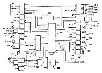
Fig. 13 illustrates a block diagram of the
electrical system of the instrument of Fig. 1;
Fig. 14 illustrates a schematic diagram of an
electric circuit of the instrument of Figs. 1 and 13;
Figs. 15a-b illustrate a schematic diagram of an
electric circuit of the instrument of Figs. 1 and 13;
Fig. 16 illustrates a reflected light signal and
a rectified reflected light envelope according to the
present invention;
Figs. 17a-b illustrate enlarged fragmentary
longitudinal sectional views taken generally along section
lines 17-17 of Fig. 4;
Fig. 18 illustrates a detected light profile
according to the present invention; and,
Fig. 19 illustrates two waveforms useful in
understanding a start noise immunization technique employed
in an instrument constructed according to the present
invention.
Models) for Carryinct Out the Invention
The following schematic and block circuit diagram
descriptions identify specific integrated circuits and
other components and in many cases specific sources for
WO 95/07452 5 ~ PCTlUS94/09505
_g_
these. Specific terminal and pin names and numbers are
generally given in connection with these for the purposes
of completeness. It is to be understood that these
terminal and pin identifiers are provided for these
specifically identified components. It is to be understood
that this does not constitute a representation, nor should
any such representation be inferred, that the specific
components or sources are the only components available
from the same or any other sources capable of performing
the necessary functions. It is further to be understood
that other suitable components available from the same or
different sources may not use the same terminal/pin
identifiers as those provided in this description.
An instrument 100 for determining the coagulation
time of a specimen, whether of blood or of a control,
includes a housing 102 comprising a housing bottom 104 and
a housing top 106. Top 106 is provided with a battery door
108 which covers a battery well 110 housing the instrument
100's battery power source (not shown). Bottom 104 houses
a Kyocera KBS26DA7A piezoelectric beeper 112, and a printed
circuit board (PCB) 114 onto which are assembled various
circuit components which will be described later. An
optics assembly 116, a socket 118 for a test parameters
electronically erasable programmable read-only memory
(EEPROM) key 119 of the type described in U.S. Patent 5,
053,199, a socket 120 for serial data communication, and a
power supply connector 122 for connection of instrument 100
to an external AC/DC adapter (not shown) for operation
thereby in lieu of the batteries (not shown) with which
instrument 100 is typically equipped, are also assembled
onto PCB 114.
Optics assembly 116 includes a covered 126 strip
adapter top assembly 132 hinged 128 to a strip adapter
bottom assembly 130. Strip adapter bottom assembly 130
includes a magnet assembly 140 held to bottom assembly 130
WO 95/07452 ~ ~~ PCT/US94/09505
-10-
by a spring clip retainer 142. Magnet assembly 140
includes an 850 turn (#32 A.W.G.) coil 144 wound on a
bobbin 146 which is positioned over the center leg 148 of a
50% nickel/50% iron powdered metal E-core 150. The end
legs 152 of E-core 150 lie outside coil 144. A
nine-and-one-half pole per end, flat plate, barium ferrite
bias magnet 154 is placed over the end of the center leg
148 and is supported on one end of the bobbin 146. A
connector 156 permits electrical connections to be made to
coil 144.
Strip adapter bottom assembly 130 also includes a
sample port housing assembly 160 having a housing 162
within which are mounted a Siemens type BPW34F photodiode
164 and a Honeywell type SEP8705-003 LED 166. Photodiode
164 senses light generated by LED 166 and reflected from
the sample and strip 101 to provide an indication that a
sample, be it blood or control, has been applied to
instrument 100 for testing. A connector 168 provides for
electrical connections to photodiode 164 and LED 166. A
clamp 170 retains LED 166 in housing 162. The angle
between the axes of the LED 166 and photodiode 164 openings
172, 174, respectively, is about 15°.
Strip adapter bottom assembly 130 also includes a
heater assembly 180 including a heater foil 182 constructed
from two Kapton/WA polyamide films between which is
sandwiched a copper nickel foil trace 183. A thermal fuse
184 and a thermistor 188 are mounted on the side of the
foil 182 opposite the heater trace. Thermal fuse 184 is
coupled through the foil 182 between one terminal 186 of
the heater foil trace and the - HEATER terminal of a heater
circuit. Contact is made to the leads of thermistor 188
from the THermistor + and - leads of the heater circuit
through a hole 190 in the foil 182. An aluminum nitride
heater plate 192 having a light reflecting top surface 194
is attached to foil 182 over the heater pattern area 193 of
WO 95/07452 PCT/US94/09505
-11-
the heater trace using a thermosetting acrylic adhesive.
Electrical connections are made to heater assembly 180
through a connector 196.
A transparent polycarbonate window 200 is
adhesively attached to a region 202 of strip adapter bottom
assembly housing 203 which is formed with a series of eight
transversely extending slit openings 204-1 -- 204-8,
respectively. A transparent polycarbonate window 206 is
provided with an opaque glossy black coating 208 over part
of its surface and an opaque glossy yellow coating 210 over
part of its surface. The remainder 211 of window 206
remains transparent. Remainder 211 overlies a slit 213 in
housing 203 through which radiation from LED 166 is
transmitted to the sample and through which remission from
the sample is detected by photodiode 164. The yellow
region 210 visible to the user of instrument 100 indicates
where the sample, be it blood or control, is to be placed
on a transparent disposable strip 101, such as those
illustrated and described in U.S. Patent 4,849,340 or the
CoaguChekT" coagulation system test strip available from
Boehringer Mannheim Corporation, 9115 Hague Road,
Indianapolis, Indiana 46250, when the disposable strip 101
is properly located in the optics assembly 116. A
push-button latch 214 including a button 216 biased into
locking position by a scissors-shaped compression spring
218 completes strip adapter bottom assembly 130.
Strip adapter top assembly 132 includes a strip
adapter top 222 into which is mounted a Centronic type
4500094 bar code reading photodiode 224 with an elongated
active region exposed through a slot 226 and a transparent
polycarbonate window 228 adhesively mounted on the
underside of top 222 to close slot 226. A photosensor
bracket 230 captures photodiode 224 in position adjacent
slot 226. Test strip clamps containing foam springs 232,
useful in pressing test strip 101 against heater plate 192,
WO 95!07452 ~ ~ 6 ~ g ~~ PCT/US94/09505
-12-
have tabs that fit into locating openings provided therefor
in the floor of top 222. Space 235 is provided between
clamps 232 to accommodate a positioning bracket 236 which
is mounted on the underside of PCB 234 and extends downward
therefrom into space 235. Siemens type SFH405-3 START LED
238 and FILL LED 240 are mounted respectively in front of
and behind positioning bracket 236 angled at about 5° to
the normal plane of incidence on PCB 234. A Siemens type
BPW34F photodiode 242 with a daylight filter is mounted on
PCB 234 inside positioning bracket 236. All three of
components 238, 240, 242 are exposed downward through
openings provided therefor in the bottom of strip adapter
top 222 of the strip adapter top assembly 132. An Optek
type OP290A MAIN assay LED 244 is mounted in an opening 246
provided therefor in strip adapter top 222 and is held in
place by a holding clamp 248. The leads of LED 244 are
connected to PCB 234. The axis of opening 246 makes an
angle of about 45° with the axis of the opening for
photodiode 242 and intersects it.
A pop-up bracket 250 is spring 252-loaded into an
opening provided therefor in a rear end wall 254 of strip
adapter top 222 to cause the strip adapter top assembly 132
to pop up when button 216 is pushed. An eleven-conductor
flat cable 256 and connector 258 make the connections
between the components mounted on PCB 234 and the remaining
circuits of the PCB 114. Pawl-type catches 260 extend
downward from the two forward corners of strip adapter top
222. Openings 262 are provided adjacent the front corners
of strip adapter bottom assembly 130 to accommodate catches
260. Cooperating tongues 263 on button 216 are urged into
engagement with catches 260 by spring 218 when strip
adapter bottom assembly 130 and top assembly 132 are closed
together. A flag 264 which extends downward from a side
edge of strip adapter top 222 extends into a slot 266
provided for this purpose in strip adapter bottom assembly
WO 95/07452 PCT/US94/09505
~1 b88~~
-13-
130 where flag 264 interrupts a light path from a source to
a detector to indicate that the strip adapter top and
bottom assemblies 132, 130, respectively, are closed
together.
The electrical circuitry on PCB 114 powers and
reads the various sensors included on the coagulation
optics circuit 270 on PCB 234. +5V and -5V are supplied to
circuit 270 through terminals 258-5 and 258-1,
respectively, of connector 258. Unregulated voltage is
supplied to terminal 258-8 of connector 258. Ground for
circuit 270 is provided at terminals 258-2, 4 and 7 of
connector 258. A 1~F, 25V capacitor is coupled across
terminals 258-8 and 258-2, 4, 7. The anodes of LEDs 238,
240, 244 are all coupled to terminal 258-8. The cathode of
LED 238 is coupled to the START terminal, terminal 258-11,
of connector 258. The cathode of LED 240 is coupled to the
FILL terminal, terminal 258-10, of connector 258. The
cathode of LED 244 is coupled to the MAIN terminal,
terminal 258-9, of connector 258.
The anodes of photodiodes 224, 242 are coupled
through a 100Ki1 resistor 273 to terminal 258-1. The
cathode of photodiode 242 is coupled to the - input
terminal of an operational amplifier 274. The + input
terminal of operational amplifier 274 is coupled to the
anodes of photodiodes 224, 242. The output terminal of
operational amplifier 274 is coupled to its - input
terminal through a parallel RC feedback circuit including a
560 pF capacitor and a 2.21Mtt, 1%, 50 parts-per-million
thermal coefficient resistor. The output terminal of
operational amplifier 274 is also coupled to the DETect
terminal, terminal 258-3, of connector 258.
The cathode of photodiode 224 is coupled to the -
input terminal of an operational amplifier 278. The +
input terminal of operational amplifier 278 is coupled to
the anodes of photodiodes 224, 242. The output terminal of
WO 95/07452 ~ 8 8 5 9 PCTIUS94/09505
-14-
operational amplifier 278 is coupled to its - input
terminal through a parallel RC feedback circuit including a
.001~,F capacitor and a 499Kf2, 1% resistor. The output
terminal of differential amplifier 278 is also coupled to
the CodeBaR OUTput terminal, terminal 258-6, of connector
258. Operational amplifiers 274, 278 illustratively are
National Semiconductor type LPC662IM operational
amplifiers.
A +V terminal of a National Semiconductor type
LM385M-2.5, 2.5V reference voltage source 279 is coupled to
terminals 258-2, -4 and -7 of connector 258. The -
terminal of reference voltage source 279 is coupled to the
anodes of photodiodes 224, 242, to the + input terminals of
operational amplifiers 274, 278, and through resistor 273
to the -5V terminal, 258-1, of connector 258.
The electric circuitry 280 mounted on PCB 114
processes the various signals from circuitry 270, as well
as others which circuitry 280 generates itself or receives
from the user of instrument 100, or which are generated
externally to instrument 100. An Intel type N83C51FC
eight-bit microcontroller (~,C) 284 has data terminals
P0.0 - P0.7 coupled to DATA lines 0-7, respectively, of an
instrument 100 bus 286. ACC 284 address terminals
P2.0 - P2.4 and P2.6 - P2.7 are coupled to address lines
A8-A12 and A14-A15, respectively, of bus 286. The Reap and WR
terminals, P3.7 and P3.6, respectively, of ~,C 284, are
coupled to the Rea Data and Write Data lines,
respectively, of bus 286. An Address Latch Enable terminal
of ~C 284 is coupled to the ALE terminal of a Toshiba type
TCi1L003AU-1031 application specific programmable gate
array integrated circuit (ASIC) 290. The TIP (transmit)
terminal 120-2 of serial data port socket 120 is coupled
through the parallel combination of a 120pF capacitor and a
220Kft resistor to ground, and through a lOKn series
resistor to the Transmit Data (TXD) terminal P3.1 of ~,C
WO 95/07452 PCTIUS94/09505
21 ~~85~
-15-
284. The RING (receive) terminal 120-3 of serial data port
socket 120 is coupled through the parallel combination of a
120 pF capacitor and a 220Kf1 resistor to ground and through
a l.2Kft series resistor to the Receive Data (RXD) terminal
P3.0 of ~C 284. The GrouND terminal 120-1 of socket 120 is
coupled to ground.
The CS terminal 118-1 of ROM key socket 118 is
coupled through a Philips type BZV55C6V2 6.2V Zener diode
to ground and directly to a Code ROM IC chip Select Output
terminal 22 of ASIC 290. The SK terminal, 118-2, of ROM
key socket 118 is coupled through a type BZV55C6V2 Zener
diode to ground and directly to the CLOCK terminal,
terminal P1.0, of ~,C 284. It is also coupled to the SK
terminal of a Samsung type 93C46AK EEPROM 292 internal to
instrument 100. EEPROM 292 generally contains the meter
100 characterizing parameters. The DI and DO terminals,
terminals 118-3 and 4, of socket 118 are coupled to each
other, to ground through a BZV55C6V2 Zener diode, directly
to the DI and DO terminals o.f EEPROM 292, and directly to
the EEDI/DO terminal P3.5, of ~.C 284. Terminal 118-5 of
socket 118 is coupled to ground. Terminal 118-8 of socket
118 is coupled to the system +5V supply.
The time base for ~,C 284 is generated by a 7.3728
MHz crystal which is coupled across terminals X1-X2
thereof. A 27pF capacitor is coupled between each terminal
of the crystal and ground. Terminal P1.5 of ACC 284 is
coupled to a resistive voltage divider including two series
100Kf1 resistors in a beeper 112 driver circuit 294. The
common terminal of the series 100Kft resistors is coupled to
the base of a Siemens type BC848C driver transistor 296.
The collector of transistor 296 is coupled through a lKft
pull-up resistor to +5V and directly to one terminal of
beeper 112. The emitter of transistor 296 and the other
terminal of beeper 112 are both coupled to ground. Two
WO 95/07452 216 ~ 8 5 ~9 PCTNS94109505
-16-
type LL4148 diodes clamp the collector of transistor 296
between ground and +5V.
The data terminals Do-D7 of a Samsung type
LH5164-10 8K by 8 static random access memory (SRAM) 300
are coupled to the DATA 0-DATA 7 lines, respectively, of
bus 286. The address terminals AO-A12 of SRAM 300 are
coupled via the system bus 286 to the AO-A7 terminals of
ASIC 290 and the A8-A12 terminals of ~C 284, respectively.
The Reap and WR terminals of SRAM 300 are coupled via
the bus 286 to the Reap and WR terminals, respectively,
of ~.C 284. The CE2 terminal of SRAM 300 is coupled to the
junction of a 390Kt1 resistor and a .1~F capacitor. The
other terminal of the resistor is coupled to +5V. The
other terminal of the capacitor is coupled to ground. The
CE2 terminal is clamped via a type LL4148 diode to +5V.
The DATA 0-DATA 7 terminals of a Samtron type UC16203GNAR
two line by sixteen character display 302 are coupled to
the DATA 0-DATA 7 terminals of bus 286. The DISPlay ENable
terminal of display 302 is coupled via bus 286 to the
DISPlay ENable terminal of ASIC 290. The AO-A1 terminals
of display 302 are coupled to the AO-A1 terminals,
respectively, of bus 286. The GrouND terminal of display
302 is coupled to the system ground and the VDD terminal of
display 302 is coupled to +5V. Terminal 3 of display 302
is coupled through a 1KS1 resistor to ground and through an
l8Kn resistor. to +5V. An instrument 100 keypad switch has
its ON/OFF terminal connected to the source of a Samsung
type BSS139 field effect transistor (FET) 303 in instrument
100's power supply circuit 304. The YES terminal of the
switch is coupled to Input terminal 1 of ASIC 290. The NO
terminal of the switch is coupled to Input terminal 2 of
ASIC 290. The YES and NO terminals are also coupled
through respective 1Mn pull-up resistors to +5V.
Battery back-up protection is provided to SRAM
300 by a circuit including a 3.3V regulator 306. The V~,
PCT/LTS94/09505
WO 95107452 2 ~ 6 g 8 5 ~
-17-
terminal of regulator 306 is coupled to the junction of a
resistor and a capacitor. The other terminal of the
capacitor is coupled to ground. The other terminal of the
resistor is coupled to the cathode of a diode, the anode of
which is coupled to +VBAT. The V,~, terminal of regulator
306 is coupled across a series resistive voltage divider
including a resistor 308 and a resistor 310 to ground.
is also coupled to the emitter of a transistor 312. The
junction of resistors 308, 310 is coupled to the base of a
transistor 314. The emitter of transistor 314 is coupled
to ground. Its collector is coupled through a series
resistor to the base of transistor 312. The collector of
transistor 312 is coupled to the BATtery 1 terminal of a
real time clock 316, and to one terminal. of a capacitor,
the other terminal of which is coupled to ground. The D
and Q terminals of IC 316 are coupled to the DATA 0 line of
bus 286. The ~, CEO , WE and OE terminals of IC 316 are
coupled to terminal P2.7(A15) of ~,C 284, terminal CE of
SRAM 300, the Write ata line of bus 286, and the Rea Data
line of bus 286, respectively. The VCC OUTPUT terminal of
IC 316 is coupled to the VDD terminal of SRAM 300 and
through a capacitor to ground. The time. base for IC 316 is
generated by a crystal coupled across terminals X1-X2
thereof.
The PoWeR INTerrupt, MAIN ConTroL, HeaTeR ON/OFF,
A/D OUT, A/D A, A/D B, power SUPPLY ON, SAMPLE ConTroL, and
MAGnet 1 ConTroL terminals, terminals P3.2, P3.3, P3.4,
P1.1, P1.2, P1.3, P1.4, P1.6 and P1.7, respectively of ~C
284, are coupled to the power supply circuit 304, the main
LED driver in an LED driver circuit 320, the heater control
circuit 322, the COMParator OUTput terminal of a Teledyne
type TSC500ACOE A/D converter IC 324 in the analog section
of instrument 100, the A terminal of A/D 324, the B
terminal of A/D 324, power supply circuit 304, the sample
WO 95/07452 PCT/US94/09505
z~ 68s59
-18-
port circuit 326, and the magnet current control circuit
328.
The Input 3 terminal of ASIC 290 is coupled to an
Omron type EE-SX 1067 optical switch 486. The Output 10-17
terminals of ASIC 290 are coupled to the bar code LED array
driver circuit 330. The Output terminals 20, 21, 24 and 25
of ASIC 290 are coupled to the setpoint temperature control
of heater driver circuit 322, the LATCH ENABLE terminal of
a Signetics type 74HC4351DW eight-to-one analog multiplexer
332 in the analog section of instrument 100, the fill LED
driver in circuit 320, and the start LED driver in circuit
320, respectively. The Address 0-2 lines of bus 286 are
coupled to the A, B and C terminals, respectively, of
multiplexer 332.
Power supply circuit 304 includes an instrument
100 battery connector 334 having +VBAT terminal 334-1 and
ground terminal connector 334-2 and AC/DC converter power
supply connector 122 having +VIN terminals 122-3 and 6
connected together and GRouNd terminals 122-1 and 4
connected together. +VBAT is coupled through a series
resistor to the gate of FET 303. The drain of FET 303 is
coupled through two series resistors 336, 338 to the base
of a transistor 340. The emitter of transistor 340 is
coupled to its base through the series combination of a
resistor and a diode, through a diode and 2.0 ampere fuse
to +VIN, and through a parallel combination of a transient
suppressor diode, a resistor and a capacitor to ground.
The junction of resistors 336, 338 is coupled through a
resistor to the base of a transistor 342. The emitter of
transistor 342 is coupled to the base of transistor 340.
The collector of transistor 342 is coupled through two
series resistors to ground. The common terminal of these
resistors is coupled to the base of a transistor 346. The
emitter of transistor 346 is coupled to ground and its
collector is coupled through a pull-up resistor to +5V.
WO 95/07452 PCT/US94/09505
z~ 68s5~
-19-
The collector of transistor 346 is also coupled to Input
terminal 0 of ASIC 290.
The emitter of a transistor 350 is coupled to
+VBAT. +VBAT is coupled through a resistor and a diode in
series to the base of transistor 350. The base of
transistor 350 is coupled through a diode 351 to the base
of transistor 340. The base of transistor 340 is coupled
through a parallel resistance network to the collector of a
transistor 352. The emitter of transistor 352 is coupled
to ground. Its base is coupled through a resistor to
ground and through a resistor to the collector of a
transistor 354. The emitter of transistor 354 is coupled
to +5V Analog. The base of transistor 354 is coupled
through a resistor to +5VA. The base of transistor 354 is
also coupled through a resistor to terminal P1.4 of ~.C 284.
Once the on/off key to meter 100 is depressed upon turn-on,
enough time is given for the +5V supply to come up and the
~C 284 to reset itself (once +5V supply has been applied to
its V~ pin) and then to have terminal P1.4 of ~C 284 latch
the system +5V supply on. This terminal is also used to
shut the system down in an orderly fashion. VUNREGulated
appears at the collector of transistor :350 and at the
cathode of a diode 356, the anode of which is coupled to
the collector of transistor 340.
Regulation is initiated by battery voltage +VBAT
on the gate of FET 303. If the battery is in backward, or
is below minimum regulation level and na AC/DC adapter is
connected to instrument 100, or is missing and no AC/DC
adapter is connected to instrument 100, the instrument 100
cannot be turned on. If the battery is installed properly
and is above minimum regulation level, regulation is
established at the base of transistor 340 and, through
diode 351, at the base of transistor 350. Regulation is
also signalled through transistors 342 and 346 to the
ON/OFF INDicator Input terminal 0 of ASI:C 290. If the
WO 95!07452 9 PCT/US94/09505
-20-
battery voltage +VBAT is greater than +VIN, diode 356
decouples the AC/DC adapter input circuity, including
transistor 340 and its associated regulating circuitry from
VUNREGulated so that the battery does not power that
circuitry.
VUNREGulated is supplied to the VIN terminal of a
+5V regulator IC 360. VUNREGulated is also supplied to a
series voltage divider including a resistor 362 and a
resistor 364. The common terminal of resistors 362, 364 is
coupled to the INput terminal of a voltage detector IC 366.
The ERROR output terminal of IC 366 is coupled through a
resistor to VUNREGulated and through a resistor to the base
of a transistor 368. The collector of transistor 368 is
coupled through a load resistor to VUNREGulated and is
coupled directly to the SHUTDOWN terminal of +5V regulator
IC 360. If the supply voltage is low, IC 366 will prevent
instrument 100 from being turned on. Regulated +5V for the
digital circuitry of instrument 100 appears at the VOUT
terminal of +5V regulator IC 360. The SENSE terminal of
IC 360 is coupled to +5V. The ERROR terminal of IC 360 is
coupled through a pull up resistor to +5V. The ERROR
terminal is also coupled to the PoWeRINTerrupt terminal,
P3.2, of ~C 284. The error terminal's main function is to
warn the ~C 284 that the system power is approaching an
unregulated condition. By warning ~.C 284 of such
condition, ~,C 284 can power down the system in an orderly
fashion prior to any soft failures occurring. A capacitor
across VOUT and GrouND of IC 360 is decoupled by a resistor
from a tantalum capacitor across the +5 VAnalog supply to
analog ground. The voltage across the VOUT output terminal
to ground is fed back through a diode and resistor in
series to the base of transistor 368. The VOUT output
terminal of IC 360 is also coupled to the V+ terminal of a
+5V-to--5V converter 369. A tantalum capacitor is coupled
across the CAP+ and CAP- terminals of converter 369. -SVDC
WO 95/07452 PCT/US94/09505
2~b885~
-21-
for circuits requiring it appears across the VOUT terminal
of converter 369 to ground. The instrument 100's analog
and digital grounds are tied together here. A +V terminal
of a 2.5V reference voltage source 370 is coupled through a
resistor to +5 VAnalog. 2.5 VREFerence is established
across the +V terminal of source 370 and ground.
Turning now to the LED driver circuitry 320 for
the optical head assembly 116, the start LED control Output
terminal 25 of ASIC 290 is coupled through a type LL4148
diode to the - input terminal of a Samsung type LM324A
operational amplifier 374. The + input terminal of
operational amplifier 374 is coupled to VREF. The output
terminal of operational amplifier 374 is coupled to the
base of a Philips type PXT4401 transistor 376. The
collector of transistor 376 is coupled to the START LED
terminal, terminal 258-11, of connector 258. The emitter
of transistor 376 is coupled to ground through a 100f1
resistor, which limits the current through the start LED at
a constant current, and through a 100Kf1 feedback resistor
to the - input terminal of operational amplifier 374.
The FILLConTroL terminal, Output terminal 24, of
ASIC 290 is coupled through a type LL4148 diode to the -
input terminal of a type LM324A operatianal amplifier 378.
The + input terminal of operational amplifier 378 is
coupled to VREF. The output terminal of operational
amplifier 378 is coupled to the base of a type PXT4401 NPN
transistor 380, the collector of which is coupled to the
FILL LED terminal, terminal 258-10, of connector 258. The
emitter of transistor 380 is coupled through a parallel
resistor network, the effective resistance of which is 50ft,
to ground, which limits the current through the fill LED at
a constant current, and through a 100Ki1 feedback resistor
to the - input terminal of operational amplifier 378.
The MAIN ConTroL terminal, P3.3, of ~C 284 is
coupled through a type LL4148 diode to the - input terminal
WO 95/07452 ~ ~ 6 g $ ~ 9 PCT/US94/09505
-22-
of a type LM324A operational amplifier 382. The + input
terminal of operational amplifier 382 is coupled to VREF.
The output terminal of operational amplifier 382 is coupled
to the base of a Philips type PXTA14 Darlington-coupled
transistor pair 384. The collectors of transistors 384 are
coupled to the MAIN assay LED terminal, 258-9, of connector
258. The emitter of transistors 384 is coupled through a
100n 1%, 25 parts-per-million temperature coefficient
resistor to ground, which limits the current through the
main LED at a constant current, and through a 100Kf1
resistor, to the - input terminal of operational amplifier
382.
The sensed bar code of the disposable test strip
101 which is being used in a particular test comes in to
circuit 320 serially on the CodeBaR terminal, 258-6, of
connector 258. It is coupled directly to analog input
terminal X5 of multiplexer 332. The START, FILL and MAIN
assay DETect signals indicating that an adequate volume
sample droplet has been placed over yellow area 210 on a
test strip 101, and its raw coagulation results data, are
provided from terminal 258-3 of connector 258 to the +
input terminals of two type LM324A operational amplifiers
386, 388. Operational amplifier 386 is configured as a
unity gain buffer and its output terminal is coupled to the
DC input terminal X1 of multiplexer 332. Operational
amplifier 388 is also configured as a unity gain buffer and
its output terminal is capacitively coupled through a .1~F
capacitor and two series 100Kn resistors 390, 392 to a +
input terminal of a type LPC662IM operational amplifier
394. The output terminal of operational amplifier 388 is
also coupled to ground through an RC parallel combination
of a l.5Mt1 resistor and .0033~.F capacitor. The + terminal
of operational amplifier 394 is coupled to ground through a
.056~F capacitor. The output terminal of operational
amplifier 394 is coupled through a 2Mil, 1% feedback
WO 95/07452
PCT/US94/09505
-23-
resistor to its - input terminal. Its -- input terminal is
coupled to ground through a 221Ktt, 1% resistor. The output
terminal of operational amplifier 394 is also coupled
through series 100Kn, 1% and 20Kf1, 1% resistors 396, 398,
respectively, to ground. The common terminal of resistors
396, 398 is coupled through a .056uF capacitor to the
common terminal of resistors 390, 392.
The signal at the output terminal of operational
amplifier 394 is directly coupled to the XO input terminal,
ACl, of multiplexes 332. That signal is also coupled to
the + input terminal of a type LPC662IM operational
amplifier 400. The signal at the output. terminal of
operational amplifier 400 is directly coupled to the X2
input terminal, AC2, of multiplexes 332. The output
terminal of operational amplifier 400 is also coupled
through a 3Mft, 5% resistor to the - input terminal thereof.
The - input terminal of operational amplifier 400 is
coupled through a lMtl, 5% resistor to ground.
VUNREGulated is coupled through a series voltage
divider including a resistor 402 and a resistor 404 to
ground. The common terminal of resistors 402, 404 is
coupled directly to the analog BATTery voltage input
terminal X4 of multiplexes 332. +5VA is coupled to the VDD
input terminal of a temperature sensor 406. The VOUT
terminal of sensor 406 is coupled directly to the analog
VTEMP voltage input terminal, X6, of multiplexes 332 and
through a pull-up resistor to +SVA.
The heater control circuit 322 includes two
series resistors 410, 412 coupled between the HeaTeR ON/OFF
terminal of ~C 284 and ground. The common terminal of
resistors 410, 412 is coupled to the base of a transistor
414, the collector of which is coupled through two series
resistors 416, 418 to +SVA, and the emitter of which is
coupled to ground. The common terminal of resistors 416,
418 is coupled to the base of a transistar 420, the emitter
WO 95107452 ~ PCT/US94109505
-24-
of which is coupled to +SVA, and the collector of which is
coupled through a series resistor 422 and capacitor 424 to
ground. The common terminal of resistor 422 and capacitor
424 is coupled to the - input terminal of an operational
amplifier 426.
+5VA is coupled through a series resistor, a
potentiometer 428 and a resistor to ground. The movable
contact of potentiometer 428 is coupled to the - input
terminal of operational amplifier 426. The potentiometer
enables the heater plate 192 to achieve about 39°C. +5VA
is coupled through a series resistor 430 and capacitor 432
to ground. The common terminal of resistor 430 and
capacitor 432 is coupled to the THermistor + terminal,
196-3, of connector 196, and to the + input terminal of
operational amplifier 426. The + input terminal of
operational amplifier 426 is coupled through the series
combination of a diode and a resistor to ground. The
junction of the resistor and diode is coupled to the base
of a transistor 434, the emitter of which is coupled to
ground. The output terminal of operational amplifier 426
is coupled through a resistor to its - input terminal and
through the series combination of a diode and a resistor to
the collector of transistor 434.
The SETPoinT 2 terminal, Output terminal 20, of
ASIC 290, is coupled through series resistors 436, 438 to
+SVA. The ASIC 290 provides control of the heater plate
192 temperature at two different setpoints, 39°C and 44°C.
The second setpoint is set high to permit the heater plate
192 to attain 44°C temperature, thereby permitting more
rapid warming of samples to 39°C. The common terminal of
resistors 436, 438 is coupled to the base of a transistor
440, the emitter of which is coupled to +5VA and the
collector of which is coupled through a resistor to the -
input terminal of operational amplifier 426. A series
resistive voltage divider including a resistor 442 and a
WO 95/07452 ~ ~ ~ PCT/IJS94/09505
-25-
resistor 444 is coupled between the output terminal of
operational amplifier 426 and ground. 'The common terminal
of resistors 442, 444 is coupled to an analog input
terminal X3 of multiplexer 332. Heater control circuit 322
operating status is thus multiplexed into ~,C 284.
Additionally, heater control status, as reflected by the
voltage at the collector of transistor 434, controls the
flow of current through the heater foil 182. This is
accomplished through a transistor 446, the base of which is
coupled to the collector of transistor 434 and the
collector of which is coupled to the - HEATER terminal,
196-2, of connector 196. The + HEATER terminal, 196-1, of
connector 196 is coupled to + VUNREGulated. The emitter of
transistor 446 is coupled through a parallel resistance
network to ground. The base of transistor 446 is also
coupled through two series diodes to ground, which limits
the current through the heater foil to approximately 0.4A.
The - THermistor terminal, 196-4, of connector 196 is
coupled to ground.
Terminal P1.6 of ~cC 284 is coupled through a type
LL4148 diode to the - input terminal of a type LM324A
operational amplifier 450 in the sample port circuit 326.
The + input terminal of operational amplifier 450 is
coupled to VREF. The output terminal of operational
amplifier 450 is coupled to the base of a type BC848C NPN
transistor 452, the emitter of which is coupled through a
100Kft feedback resistor to the - input terminal of
operational amplifier 450 and to ground through 6011
resistance, which limits the current through the sample
port LED at a constant current. The collector of
transistor 452 is coupled to terminal 168-1 of the sample
port connector 168. +5VA is coupled to terminal 168-2, the
VDD terminal, of connector 168. VUNREGu.lated is coupled to
terminal 168-5 of connector 168. The SAMPle IN terminal,
168-4, of connector 168 is coupled to ground through a
WO 95/07452 a ~ 6 g a 59 pCT/US94/09505
-26-
20Kft, 1% resistor and through a .OO1~F capacitor to the -
input terminal of a type LPC662IM operational amplifier
456. The + input terminal of operational amplifier 456 is
coupled to ground. The output terminal of operational
amplifier 456 is coupled through a parallel RC feedback
circuit including a 200Kf1, 1% resistor and a 39pF capacitor
to its - input terminal. The output terminal of
operational amplifier 456 is coupled through a .0047~F
capacitor to the + input terminal of a type LPC662IM
operational amplifier 458. The + input terminal of
operational amplifier 458 is coupled to ground through a
15Kt1, 1% resistor.
The - input terminal of operational amplifier 458
is coupled to ground through a 20Kn, 1% resistor. The
output terminal of operational amplifier 458 is coupled to
the cathode of a type LL4148 diode, the anode of which is
coupled through a 100Kf1, 1% resistor to the - input
terminal of operational amplifier 458. The output terminal
of operational amplifier 458 is also coupled to the anode
of a type LL4148 diode 460, the cathode of which is coupled
through a iMn, 1% resistor 462 to the - input terminal of
operational amplifier 458. This provides a hysteresis-type
configuration which has different gains depending upon
whether the voltage at the + input terminal of operational
amplifier 458 is greater than or less than the voltage at
the - input terminal thereof. The common terminal of diode
460 and resistor 462 is coupled through the series
combination of a lKfl, 1% resistor 464 and a .047~,F
capacitor 466 to ground. The common terminal of resistor
464 and capacitor 466 is coupled to the SAMPle DETect input
terminal, X7, of multiplexer 332.
Terminal P1.7 of ~,C 284 is coupled through two
series resistors in the magnet control circuit 328 to
ground. The common terminal of these resistors is coupled
to the base of a transistor 470, the emitter of which is
WO 95/07452 PCT/US94/09505
21 b 8859
-27-
coupled to ground. The collector of transistor 470 is
coupled through series resistors to +SVA. The common
terminal of these resistors is coupled to the base of a
transistor 471, the emitter of which is coupled to +5VA and
the collector of which is coupled to the - input terminal
of an operational amplifier 472. The series combination of
a resistor 474 and a resistor 476 is coupled between VREF
and ground. A capacitor is coupled across resistor 476.
The common terminal of resistors 474 and 476 is coupled to
the + input terminal of operational amplifier 472.
The output terminal of operational amplifier 472
is coupled to the base of a magnet coil 144-driver
transistor 478. The emitter of transistor 478 is coupled
through a resistor to ground, which limits the current
through the magnet coil at a constant current, and through
a feedback resistor to the - input terminal of operational
amplifier 472. A capacitor is coupled between the - input
terminal of operational amplifier 472 and ground. The
collector of transistor 478 is coupled to terminal 156-3 of
connector 156. Terminal 156-1 of connector 156 is coupled
to VUNREGulated. Coil 144 is coupled across connectors
156-1 and 156-3. The series combination of a resistor and
a capacitor is also coupled across connectors 156-1 and
156-3. A flyback diode is also coupled across terminals
156-1 and 156-3.
The bar code LED driver circuit 330 which is
associated with photodiode 224 includes eight Stanley type
BR1102W bar code-illuminating LEDs 484-1.--484-8. The anode
of LED 484-1 is coupled to +5V and its cathode is coupled
to the Anode terminal of optical switch 486. Optical
switch 486 provides the source and detector for flag 264 to
indicate when the strip adapter top and bottom assemblies
130, 132 are closed together. The collector terminal, C,
of optical switch 486 is coupled to Input terminal 3 of
ASIC 290, and through a 100Kft load resistor to +5V. The
CA 02168859 2006-07-26
78807-1.
_28_
cathode terminal, K, of optical switch 486 is coupled
through a 120n load resistor to the collector of a type
BC848C NPN transistor 490-1, the emitter of which is
coupled to ground and the base of which is coupled through
a lOKn resistor to Output terminal 17 of ASIC 290. The
anodes of the remaining LEDs 484-2--484-8 are coupled
through a common 60n load resistance to +5V. The cathodes
of LEDs 484-2--484-8 are coupled to the collectors of type
BC848C NPN transistors 490-2--490-8, respectively. The
emitters of transistor 490-2--490-8 are coupled to ground.
The bases of transistor 490-2--490-8 are coupled through
respective lOKn resistors to Output terminals 16-10,
respectively, of ASIC 290.
LEDs 484-1--484-8 are mounted on PCB 114 and emit
15. light through respective slit openings 204-1--204-8,
respectively. LED's 484-1--484-8 are sequentially
energized through transistors 490-1--490-8, respectively.
The presence or absence of a bar code in region 492 of a
particular test strip 101 placed in instrument 100 is
sensed by transmission of light from a respective LED
484-1--484-8 by conduction of photodiode 224. This
identifies certain test strip 101 lot-specific parameters
for instrument 100. It further permits the code in region
492 to be compared to data stored in the non-volatile
memory of ~;ey 119 and the instrument 100 to be disabled if
the comparison of the code in region 492 to the data stored
in the non-volatile memory of key 119 is unfavorable.
Industrial Agplicability
In operation, a sample 514 is deposited in the
test strip 101 sample well 494 over location 210.
Radiation from LED 166, which is strobed at .25 sec.
intervals, detected by photodiode 164 establishes the
dosing of strip 101. START LED 238 is strobed at 50 msec.
intervals until the arrival of the sample 5i4 at the region
of strip 101 over START LED 238 is established by the
radiation from START LED 238 detected by photodiode 242.
21 b8859 '~~T~~~'~1 ~ 9.4~
~~~Al~~
-29-
The flow time of the sample 514 between the sample
application point at well 494 and the detection of the
arrival of the sample 514 over the START LED 238
establishes the sample 514 as blood or a control. The
control solutions, being less viscous, :flow between these
two locations more rapidly, and this is detected by the
instrument 100. The minimum flow time that the instrument
100 will interpret as blood and/or the maximum flow time
that the instrument 100 will interpret as control can be
varied from strip lot to strip lot by changing (a)
parameters) in the user-insertable EEPROM key 119. This
relieves the user from the need to indicate to the
instrument 100 or otherwise record when a quality control
check is being conducted.
After photodiode 242 has detected the arrival of the
sample 514 over the START LED 238, the START LED 238 is
deenergized and the FILL LED 240 is energized. The next
decrease in radiation detected by photodiode 242 indicates
the arrival of the sample 514 over the FILL region of the
strip 101. The elapsed time between detection by
photodiode 242 of arrival of the sample 514 over START LED
238 and detection by photodiode 242 of arrival of the
sample 514 over FILL LED 240 is used by the instrument 100
to determine whether the volume of the sample 514 which was
applied is adequate to conduct a coagulation test. If the
instrument 100 determines that the applied sample 514
volume was inadequate to conduct a test, the instrument 100
provides an error message and returns to its ready state.
If the instrument 100 determines that the applied sample
514 volume was sufficient to conduct a coagulation time
test reliably, FILL LED 240 is deenergized and MAIN assay
LED 244 is energized. Electromagnet 140 is also energized
and monitoring by photodiode 242 of MAIN assay LED 244
radiation begins. Magnet assembly 140, when driven by
magnet current control circuit 328, stirs ferromagnetic
particles from the test strip 101 borne by the sample 514,
be it blood or control. The particles reorient themselves
Sivrw _ ._
CA 02168859 2006-07-26
78807-1
-30-
along the combined lines of force of magnet assembly 140
and bias magnet 154 and provide a modulated light
transmission profile of the sample. This transmission
profile, illustrated in Fig. 16 at 500, is detected by
photodiode 242 and is multiplexed (DETect--AC1-DC) via
multiplexer 332 and A/D 324 into ~C 284. Coagulation of
the sample causes the reduction in the modulation in this
transmission profile as described in U.S. Patents 4,849,340
and 5,110,727. Waveform 500 is rectified and the envelope
502 of the rectified waveform 500 is formed.
To reduce the likelihood of double dosing the strip
101, the ratio of START to FILL time-to-sample application
to START time is formed. This ratio is compared to a
parameter provided from key 119. The ratio must be less
than the parameter. Otherwise the instrument 100 will
conclude that the strip 101 has been double dosed and will
generate an error message. Double dosing is to be avoided
because it can refluidize the ferromagnetic particles,
producing an erroneous coagulation time reading.
Figs. 17a-b are much-enlarged fragmentary longitudinal
sectional views of a strip 101 taken along section lines
17-17 of Fig. 4. Generally, in the absence of liquid
blood, a blood fraction or control (Fig. 17a), the indices
of refraction of the strip bottom 506 and top 508 and the
air-filled sample volume 510 between them are such that the
level of light from LED 166 returning to photodiode 164 is
relatively higher. This is illustrated at region 512 of
Fig. 18. A liquid sample 514, be it blood, a blood
fraction or a control, is deposited into the sample well
494 of strip 101 and migrates into region 510 of strip 101
over region 211 of instrument 100. Owing generally to the
matching of the strip bottom 506's, top 508's and liquid
514's indices of refraction and absorption in the case of
clear liquids, and generally to absorption and scattering
effects in the case of whole blood, a relatively lower
light level is detected by photodiode 164 as illustrated at
region 522 in Fig. 18 when a liquid is present on strip 101
~~68859 PCT~~ 94/09505
IPEii/US 3 ~ AUG 1996
-31-
adjacent region 211, This optical detection scheme permits
a clear control to be used.
Fig. 19 illustrates two waveforms useful in
understanding the start noise immunization technique
employed in an instrument according to the present
invention. It has been experimentally determined that,
unless provisions are made in instrument 100 to prevent it,
instrument 100 can be falsely triggered by negative-going
noise spikes 526 that are generated during application of a
sample to a test strip 101. Such spikes 526 are caused
when the user accidentally taps or moves the strip 101 from
side to side or in and out of the optics assembly 116
during sample application. Such negative-going spikes 526
can be greater than the instrument 100's -60mV starting
threshold, but are typically shorter in duration than the
negative-going start signal 528 and are preceded or
followed immediately by positive-going spikes 530. This is
in contrast to the actual liquid sample signal 528 which is
only negative-going. This difference i.s used to
discriminate effectively between signal 528 and noise 526,
530. The instrument 100's START algorithm discriminates
between short (noise) 526, 530 and long (start signal) 528
duration signals using negative trend, rate of signal
change and negative threshold criteria. The flow of the
START algorithm includes the following illustrative
characteristics: three consecutive data points sampled
50msec apart must be negative relative to a reference and
have rates of signal change more negative than -
7.3mV/50msec (-30 counts of the A/D converted input signal
at .243mV/count) with an absolute signal change more
negative than the -60mV (-246 counts) instrument 100 start
threshold. The parameters stored in the EEPROM 119 then
would include a signal delta of -30 counts and a start
threshold of -246 counts.