Note: Descriptions are shown in the official language in which they were submitted.
RCV. 1~'U~i: LYA-VICE~iCEtE:\ _f)5_ _ . _ _ _ 3'_ '3'~''r'. ' 1f3:'~~ '. _ _ _
_ _ _ _ _ 't'~ _~'~JI'?t):j:31=!. _ ...'~'4~ a~ 2:39~44fi5: t# 1U
CRYSTAI~INE MULTILAYER STRUCTURE AND
MA.NUhAC'fURING METHOb THEREJF
Field of the Invention
This invention relates to a process of manuracturing
crystalline structure -and more specifically to crystalline
multilayer structures based on nitrides of group Ir7 metals,
and manufacturing method thereof.
8aakcL,round of the Invention
Gallium nitride "GaN," Aluminum nitride "A1N" and
Indium nitride "InN" are known as semiconductor compounds of
large direct energy gaps. As such they are important
electronic materials.
A1N, in the form of ceramic substrata, is applied in
high power electronic applic;atians, because of its high heat
conductivity, thermal expansion ca-efficient close to that
of silicor_, and good stability at high temperatures.
It has long been known that among the nitrides of group
IZI metals, GaN has potentially the best useful properties
as a semiconductor device. Specifically, GaN nas
semiconducting properties for temperatures up to 600°C as
compared to silicon semiconductor with temperature stability
of up to 120°G. The temperature stability and large energy
gap of GaN can provide many new high temperature
applications for electronic products. - -
A second important characteristic is that a GaN p-n
function light emitting diode ("LED") emits visible blue
light with a wavelength of approximately 4~On~:. GaN has a
high efficiency of radiative recombination, and low
dizlocation mobility. The other semiconductors which are
known to Bmit lignt in that band are silicon carbide (~iC)
and generally Av HYS semiconductors such as ZnSe and CdFZ.
However, because it is an indirect bandgap material, the
luminous efficiency of SiC is only about 0.04 luman/watt.
The AI)HYI are known to have high defect mobilities and
dislaaation densities, which reduce their useful life and
the power level at which they can operate. In contrast, it
is anticipated that LED's made from GaN would have a
1
P.'~F~DED SHEET
(ZCV . b~<)\ : t:F'A-VILE\Ctif;\ U i , _ . _ 3-' :3-:35 , : lEi : 4F3 :. ,. ,.
. . _ _ _,.'~'~ :39 L'?U:?:3 t--~_ _ _ , ~49 89 2:3:3~J4~-t-Ei5 : # L I
luminous efficiency of about 0.6 lumen/watt, and remain
extremely stable over time.
Thus-GaN and ether group III metal nitrides are viable
candidates for appli.catiens in short wavelength
optaalectronics, blue laser systems, full color display
syster..is and high temperature eleatranics.
Despite their many advantages, nitrides of gxoup III
metals including GaN have not been used extensively because
of the many difficulties involved in growing such nitrides
in bulk crystals. Their thermodynamic properties preclude
the standard techniques for the growth of bulk single
crystals, appropriate for commercial use. FoY instance, the
high melting temperature and high Nz pressure at melting, of
GaN is in the range where the compound is unstable arid
readily dissociates. Due to the high melting temperature,
the substrate crystals of GaN cannot be obtained by typical
crystal growing methods like Gzochralski or Hridgman growth
from the stoichiometric melts.
Because of the difficulties to produce substances of
2o pure crystalline nitrides of group III metals, the prior art
methods use substrates made of materials other than group
III nitrides, to develop crystalline nitrides. For example,
the nitrides of group III metals like gallium nitride,
aluminum nitride, indium nitride or their allays are
deposited on crystalline substrates at different chemical
compositions like sapphire yr silicon carbide, by Molecular
Beam EpitaXy ("MBE") or Metal Organic Chemical vapor
Deposition ("MOCVD").
Specifically atoms of group ziz metals like gallium and
atoms of nitrogen are deposited on a single crystalline
substrate by causing them to collide with the substrate. In
such known procedures gallium atoms are provided by
vaparazing liquid gallium at 2800°C. nitrogen atoms are
generated from a flow of molecular nitrogen exposed to
plasma causing its molecules to dissociate. It is also
possible to apply accelerated positive ions by using an
2
A~J~ ~i:~~~ CZ-t~='~'
- ~ ~ ~ ~ ~ ~ ~ t~<u.cr.st~ r ~r~ i i . i
_. _
electric field for the acceleration to dissociate the
nitrogen molecules.
Another prior art method for developing GaN crystal is
known as metal organic chemical vapor deposition.
Accordingly, the gallium nitride is deppsited on a sapphire
substrate, by simultaneously applying two chemical
reactions: first, decomposing amm4nia and second
=decomposing a metalarganic compound, like trimethylgallium,
which is a suitable carrier of gallium. Gallium obtained
from the decomposition of the metalorganic ccmpound and the
nitrogen derived from ammonia, are deposited on the surface
of a sapphire substrate and as a result create a two layer
structure. Using a similar method, alumfnum nitride
deposited on a sapphire substrate has been produced by using
trimethylaluminum as a source of aluminum.
Another method far producing gallium nitride crystal is
disclosed in the Polish Patent rto. lz~o99. The patent
discloses a procedure for crystalli~dtion of gallium nitride
from a gas phase by sublimation and condensation process
under high nitrogen pressure. Specifically, ac:carding to
the disclosed method gallium nitride powder sublimates at
temperatures-exceeding ~aoo°c, at nitrogen pressure higher
than 1000bar. Thereafter, galliuM nitride condensation
occurs on a sapphire substrate. The temperatuze difference
between the starting material and the substrate would not
exceed 500°G.
The procedures disclosed in prior art are therefore
mainly limited to the grow~.ng of GaN crystal or other group
III metal n~.tride crystals, on a different substrate. Such
growth procedures are knewn as hetsraepitaxy production.
The gallium nitride structures obtained by such known
heteroepitaxy procedures are of low crystalline quality.
Their half width at half maximum of the X-ray double crystal
reflection curve, known as the rocking curve, is not lower
than 200 arcsec, which is not satisfactory for many
applications.
~~r': "~ ED S~IEfT
3
0
IZC~ . ~ UV : !:~:YA-SII. fVC:HW _ Uu_ _ _ _ _ _ 3 = 'B-J~ s LEi :5U : _' _ .
_ _ _ _ _ ~'~ _aJ ('?U;3=;1=!. _ . .. ~"~'J ~~J '?3;:1:)4-l~Ei.'> : N 1'1
One main reason for the poor quality crystals of the
prior art is the difference between the lattice constants of
the substrates and the deposited layers, which causes a
strain field in the structure. The large lattice mismatch,
which is 14% for sapphire and 3.4% for SiC substrate, leads
to the creation of dislocations, cracking of the layers,
island growth and the formation of incoherent boundaries
between crystalline grains.
Another difficulty with GaN is its failure to maintain
a chemical balance or stoichiometry. Gallium nitride is not
'stoiehiometric because of the high propensity for nitrogen
atoms to leave gallium nitride crystals. Therefore,
stoichiometric nitrides free of nitrogen vacancies are
difficult to obtain. Zt is commonly believed that the high
concentration of nitrogen vacancies is the source of
numerous native donor states which arc rasgansibls for high
free electron concentration observed in group III~nitride
semiconductors.
Hslnce there is a noel for multilayer high quality group
III metal nitride crystals and conssequently n and p type
semiconductors derived from such crystals in order to
benefit from their potentially important properties.
Obtects and~ummary of the~ntion
One object of the present invention is to fabricate-a
2S crystalline multilayer gallium nitride structure.
Another object of the invention is to fabricate multi-
layer crystals based on nitrides of group ITI metals or
their alloys.
Yet a further object of thlr invention is to obtain
gallium nitride crystals with satisfactory growth and
quality which can be usrad in optoelectronics and high
temperature electronics.
A further abject of the invention is to deposit
different layers of gallium nitride upon a gallium nitride
suba5trate.
4
~"~~'~D~D SLEET
WO 95/04845 ~ ~ PCT/PL94/00008
Another object of the invention is to produce P type
gallium nitride layer to ultimately produce GaN p-n
junctions.
Additional objects, advantages and novel features of
the invention will be set forth in part in the description
which follows.
According to the present invention, the foregoing and
other objects and advantages are attained by a method for
fabricating a group III metal nitride crystal by
homoepitaxial growth. For example in order to achieve a GaN
crystal growth, a first layer is grown by melting gallium at
a temperature T1 in the range of 400-2000'C and exposing the
gallium solution to high nitrogen pressure. Instead of
nitrogen a mixture of gases containing nitrogen may also be
used to obtain a first crystalline layer during a period of
about 1 hour. Then the pressure of nitrogen or nitrogen
mixture is decreased and a second layer grows at temperature
T2 not higher than T1 until the second layer of a desired
thickness is obtained. The decrease in pressure is such
that the growth rate of the second layer is significantly
slower than the growth rate of the first layer.
Furthermore, the thickness of the second layer is much less
than the thickness of the first layer. Remarkably, a
decrease of pressure of about 200 bars or more is usually
sufficient to allow the growth of a second layer with better
crystalline quality than the first layer. The second layer
has better surface flatness, and lower concentration of N-
vacancies than the first layer. Thus the resulting
crystalline structure is of such quality that allows the
attainment of highly desired industrial applications
mentioned above. Typically the width of x-ray rocking curve
of the second layer is about 20 arcsec and the difference
between the width of rocking curves for first and second
layers is about 10 arcsec. The x-ray rocking curve
indicates an improvement by a factor of 10, over prior art
crystalline structures.
5
WO 95/04845 PCT/PL94/00008
According to another aspect of the invention, once the
first layer of GaN is formed, its position is changed.
Meanwhile, the pressure of nitrogen is decreased. The first
layer is then subjected to thermal or chemical treatment at
temperatures higher than 300~C and, finally, its surface is
covered by atoms of gallium metals present in the atmosphere
or present in the flow of nitrogen gas. The atoms of .
gallium metals can emanate from vapors, beam of atoms, metal
compounds containing gallium or metalorganic compounds
containing gallium metal. Consequently a second layer of
GaN crystal deposits on a previous layer of GaN crystal at a
significantly slower growth rate than the growth rate of the
previous layer.
Once the two layer structure is obtained according to
the present invention the next layers may be deposited by
known methods in the art like chemical vapor deposition,
molecular beam epitaxy or plasma phase epitaxy.
Other objects and advantages of the present invention
will become readily apparent to those s%illed in the art
from~the following detailed description, wherein only the
preferred embodiments have been shown and described.
BRIE' DESCRIPTION OF TAE DRAWINGS
Fig. 1 illustrates a high pressure system used to
develop group III metal nitride crystals according to one
embodiment of the present invention.
Fig. 2 illustrates the high pressure system used to
develop the crystals according to another embodiment of the
present invention.
Figs. 3a-3c illustrate the pressure-temperature curves
for GaN, A1N and InN respectively.
Fig. 4 represents the dependence of temperature, T, as
a function of position X in a sample of liquid gallium
during the crystallization of the first layer..
Fig. 5 illustrates the sample of liquid gallium during
the crystallization of the first layer.
6
WO 95/04845 ~ '"~ ~ PCT/PL94/00008
Fig. 6 illustrates the concentration of nitrogen N, as
a function of position X in the sample of liquid gallium
during the crystallization of the first layer.
Fig. 7 represents the dependence of temperature, T, as
a function of position X in the sample of liquid gallium
during the crystallization of the second layer.
Fig. 8 illustrates the sample of liquid gallium during
the crystallization of the second layer.
Fig. 9 illustrates the concentration of nitrogen N, as
a function of position X in a sample of liquid gallium
during the crystallization of the second layer.
DETAILED DESCRIPTION OF THE DRAWINGS
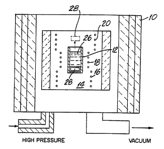
Fig. 1 illustrates a high pressure chamber 10 used
to fabricate group III metal nitride crystals of the present
15~ invention. A boron nitride crucible 12 for holding group
III metals or their alloys is placed in a three zone furnace
14, designed for work at high gas pressures of up to 20
kbar. The furnace 14 with the crucible 12 is placed in the
high pressure chamber 10. The furnace 14, consists of three
temperature zones 16, 18 and 20 supplied by electric
currents of different values. The desired pressure is
provided by adjusting the input pressure to chamber 10 by
connecting a gas compressor (not shown) to the chamber
through a high pressure inlet 22 and a vacuum outlet 24.
According to the invention, a multi-layer group III
nitride crystal is made in chamber 10. Instead of pure
group III metals discussed above, group III metal alloys can
also be used to attain a crystalline growth. Group III
metal alloys are any combination of group III metals that
result in a crystalline growth. Since III-N compounds are
fully miscible, where III is a group III metal and N is
nitrogen, many combinations of such group III metals can be
used to grow crystalline layers according to the present
invention.
A sample 26 of a metal from group III of the periodic
table or group III metal alloy as defined above is placed in
crucible 12. Thereafter the crucible is placed in the three
7
WO 95/04845 PCT/PL94/00008
zone furnace 14. The furnace with the crucible is then
placed in the high pressure chamber 10. The crucible is
placed near zone 16 with temperature Td, and zone 18 with
higher temperature Tg such that the furnace causes a
temperature gradient in the metal sample. The chamber is
filled with nitrogen gas or a gas mixture containing a
certain percentage of nitrogen. The metal sample is thus
exposed to a pressure of nitrogen or partial nitrogen
pressure. Temperatures Td and Tg are both above the metal's
melting point and the nitrogen pressure is such that the
metal sample remains in the form of a liquid solution.
During the growth of the first crystalline layer, the
pressure of nitrogen is high enough to maintain GaN
stability for the entire metal sample solution which is
exposed to heat zones 16 and 18. The first crystal layer is
grown for a period of about 5 hours. The growth period is
discretionary and depends on the desired thickness and
mechanical strength of the crystalline layer: Typically a
first layer with a thickness of few millimeters is
appropriate for many applications.
Thereafter the pressure of the nitrogen or partial
nitrogen pressure in the mixture is decreased by about 200
bars or more. With the decrease in pressure, the portion of
the sample exposed to the warmer zone 18 With temperature Tg
comes out of GaN stability range and liquid phase metal
contacts directly with gaseous nitrogen, while the portion
of the solution exposed to the cooler zone 16 with
temperature Td remains in GaN stability range. The second
crystal layer grows at temperature Td at a significantly
slower growth rate than the first layer until the second
layer of a desired thickness is obtained. The thickness of
the second layer is less than the thickness of the first -
layer and is typically around ~ micron. Therefore, although
the growth rate of the second layer is much less than the
growth rate of the first layer, the growth period necessary
to grow a second layer with a desired thickness is
s 8
WO 95/04845 PCT/PL94/00008
comparable with and in some instances less than the growth .
period of the first layer.
According to another embodiment of the invention, as
' illustrated in Fig. 2, after the first crystalline layer is
obtained, together with decreasing pressure of nitrogen, the
first crystalline layer is moved to zone 20 with temperature
Ti, which is lower than both Td and T~. Thereafter the first
crystalline layer is subjected to a chemical or thermal
treatment. At lower pressure of nitrogen, the metal
solution in crucible 12 turns into vapor~phase and begins to
evaporate towards zone 20 and in combination with nitrogen
flow causes the growth of a second layer 28 in zone 20 over
the first layer. In the alternative, the atoms of group III
metals can be obtained from vapors, beam of atoms or
compounds of these metals or from decomposition of
metalorganic compound in atmosphere or flow of nitrogen or
gases containing nitrogen.
The temperatures T~ and Td at which the metal is first
heated are in the range of 400 - 2000 C at a specified
pressure of nitrogen. The necessary pressure of nitrogen
can be determined based on the pressure-temperature curve of
the group III metal nitride.
Fig. 3(a) illustrates the pressure-temperature curve of
GaN. Fig. 3(b) illustrates the pressure-temperature curve
of A1N, and Fig. 3(c) illustrates the pressure temperature
curve of InN. The pressure-temperature curves illustrate
the minimum required pressure of N2 at different
temperatures, under which the compound remains within a
stability range. As illustrated, the higher the temperature
of the nitride compound, the higher the pressure required to
maintain the stability condition. Therefore, the area to
the left of the curves represents pressure and temperature
conditions under which no metal nitride stability is
achieved and the area to the right of the curves represents
metal nitride stability conditions.
Thus for GaN, the desired pressure of N2 at a specified
temperature T is higher than the equilibrium pressure
* 9
WO 95/04845 , PCT/PL94/00008
PW2~(T), according to the equilibrium state as illustrated by
the pressure-temperature curve of Fig. 3(a). Furthermore,
the desired pressure of N2 is preferably lower than three
times the equilibrium pressure Pw2~(T). At higher pressures '
the quality of the obtained crystal begins to deteriorate.
If the gas provided in the chamber is not pure nitrogen and '
only partially contains nitrogen, the minimum nitrogen
content in the gas mixture is preferably about 20% or more.
For AlN, the pressure of gas is in the range of 200 bar
to 10 kbar. This pressure range prevents Al evaporation and
gas phase reaction, as illustrated by the pressure-
temperature curve of Fig. 3(b). In the event that the gas
provided in the chamber only partially contains nitrogen,
the minimum nitrogen content in the gas mixture is about 1%
or more.
When pure nitrogen is used to develop a multilayer A1N
crystalline structure, the desired pressure decrease
necessary for growing the second layer with a sufficiently
slow growth rate to develop a high quality crystal layer is
about 6.4kbars. In the alternative the temperature change
is adjusted to decrease the growth rate of the second layer
with high quality characteristics. Therefore, during pure
nitrogen growth of A1N crystal the first layer is grown at
pressures of 6.5kbar or more, and the second layer is grown
at a low pressure of O.lkbar and less.
Finally for InN, the desired pressure of N2 -- similar
to GaN -- is higher than the equilibrium pressure P~2~(T),
according to the equilibrium state as illustrated by the
desired pressure-temperature curve of Fig. 3(c).
Furthermore, the pressure of N2 is preferably lower than
three times the equilibrium pressure. At higher pressures
the obtained crystal begins to deteriorate.
According to the present invention, the generation of
nitrogen vacancies in the substrate is avoided due to the
pressure growth technique disclosed herein. The
concentration of free electrons in pressure grown crystals
depends on growth temperature but also on the growth rate of
s
WO 95/04845 ~ PCT/PL94/00008
the crystal. In the crystals growing slower, this
concentration can be substantially reduced.
According to another embodiment of the present
invention, doping of the first and the second layer is
achieved by the addition of small amounts, of around 10%, of
other metals flr non-metals to the metal sample 26, in order
to introduce impurities in the growing crystalline layers.
Such impurities include Zn, Mg, Cd, Si or P. An example of
a resulting crystalline layer is a~ternary system III - X -
N, where III is a group III metal, X is an impurity and N is
nitrogen, with a solidus Which contains only one solid
phase, that is, the nitride doped with the impurity X up to
1 at.%. Group III metal alloys for growing GaN crystalline
structure may contain any combination of In, A1, Si, Mg, Zn,
Ce, Bi, and P.
Higher order crystalline structures containing more
than one impurity can also be grown. The partial group III
metal having about 10 at.% of dopants and its
crystallization by methods described above results in a
doped group III metal nitride crystal and partial
compensation of free electrons. The resulting impurity
content in the crystal is about 0.1 at.%. .
For obtaining p-type conductivity it is necessary to
reduce N-vacanies content. This is achieved by either
crystallization of the second layer from the vapor phase
described above at high NZ pressure, or by annealing an n-
type crystal doped with acceptors like Mg or Zn, at
temperatures higher than 1500°C at high N2 pressures.
Three examples for growing a multilayer group III
nitride crystal using the homoepitaxy growth of the present
invention is herein described. It can be appreciated by
those skilled in the art that the same examples are
applicable to crystal growths of AlN, InN and their alloys.
Example 1
During the operation of furnace 14, the nitrogen in the
chamber is compressed under a pressure p~ of approximately 10
11
WO 95/04845 ~ PCTIPL94/00008
kbar. The system is then heated to reach the conditions fox
growth of GaN crystals from nitrogen solution in the liquid
gallium, in a temperature gradient illustrated in Fig. 4.
Accordingly Fig. 4~illustrates the temperature T as a -
function of position X in the sample of liquid gallium in
crucible 12 during the crystallization process of the first
layer. Temperature Td of zone 16 is maintained at 1350°C and
temperature T9 of zone 18 is maintained at 1410°C. Under
pressure p~ the equilibrium temperature T~ is greater than
both temperatures Td and T~. Fig. 5 illustrates crucible 12
with 2cm3 gallium sample 26 shown in liquid form. Fig. 6
illustrates the concentration of nitrogen N, as a function
of position X in the sample of liquid gallium during the
crystallization process of the first layer. As illustrated,
the concentration of nitrogen in the liquid gallium sample
increases with the increasing temperature.
As mentioned above, the process is carried out at
conditions where GaN is stable in the entire temperature
range. Therefore, the highest temperature of the sample,
1410'C, does not exceed the equilibrium temperature (Tr) for
coexistence of three phases GaN, liquid Ga and N2 gas,
corresponding to the nitrogen pressure of 10 kbar. In these
conditions the surface of the liquid gallium begins to be
covered by a thin GaN crystalline layer. Due to the
temperature gradient in the system, nitrogen dissolved in
the warmer part of the crucible is transported, by diffusion
and convection, to the cooler part where GaN crystals in the ,
form of single crystalline hexagonal platelet grow from the
supersaturated solution as a first substrate layer. In an 8
3D hour process the crystal reaches the dimensions of 0.5 x 2 x
2mm. The next step according to the present invention is
the homoepitaxial growth of a second crystalline layer at a -
growth rate slower than the growth rate of the first layer,
in a lower supersaturation controlled by the change of
pressure and temperature of the process. Thus, the pressure
in the system is decreased by 1000 bar which changes the
distribution of concentration of nitrogen in the liquid
12
WO 95/04845 PCT/PL94/00008
gallium 26 of figure 8, based on the curve illustrated in
Fig..9. The equilibrium temperature for pressure of 9000
bar is between the temperatures of the warmer and the cooler
parts of the crucible as illustrated by Fig. 7. Under this
condition, as illustrated by Fig. 9, in the warmer part of
the crucible, gallium nitride is not stable and the liquid
phase gallium has a direct contact with gaseous phase .
nitrogen.
The solubility of the gas in Ga, in contrast to the
solubility of GaN, is a decreasing function of temperature.
The chemical potential of gas, at constant pressure,
decreases with temperature due to rapidly decreasing
density. Similarly for the same temperature as the pressure
decreases the solubility of nitrogen in Ga also decreases.
The change in temperature dependence of nitrogen
concentration in the solution leads to the lowering of the
supersaturation in the growth region of the solution. At
the conditions of this example, the average growth rate of
the layer is of order of 10-3 mm/h. The width of the rocking
curve for the layer deposited on GaN crystal is typically
20-24 arcsec. The lowering of the supersaturation and the
slower growth rate provides for the growth of a better
quality crystal.
Furthermore, during the growth of the second layer, the
part of the gallium sample with temperature T~ above the
equilibrium temperature T~ is not covered by the GaN surface
crust. The second layer grown at these conditions has
better qualities than the first substrate layer. It can be
appreciated by those skilled in the art that the decrease of
pressure.in the second step should be such that the
equilibrium temperature remains between the temperatures of
zone 16 and 18 of the furnace. Otherwise, no stable region
in the sample remains and the GaN crystal can readily
decompose.
Examine 2
13
WO 95/04845 PCT/PL94/00008
Fig. 2 illustrates the second embodiment of the
invention. The process of growth of the first gallium
nitride layer, which is the substrate crystal in the form of
the hexagonal plate, is carried out as explained above in
reference to Fig. 1, at a nitrogen pressure of approximately
kbar, in a temperature gradient provided by zones 16 and
i8, during an 8 hour crystallization process, until GaN
crystal with dimensions of 0.5 x 2 x 2mm is obtained. In
the next step of the process, the crystal is displaced to
10 temperature zone 20 in the fuinace, where~its temperature is
approximately 1250'C. Simultaneously, the pressure of
nitrogen is decreased by 2000 bar. At lower pressure
conditions, the substrate crystal is thermodynamically
stable, whereas the liquid gallium evaporates easily. As
illustrated in Fig. 3(a), the temperature 1410'C at zone 18
is higher than the equilibrium temperature necessary for GaN
stability at 8000 bar. .Then, Ga vapors are transported by
convection towards the substrate and deposited on it,
reacting with nitrogen to form the second layer of GaN.
Since the second layer is grown in N2-rich side of the phase
diagram, the resulting crystal has low concentration of N-
vacancies.
It can be appreciated by those skilled in the art that
depending on temperature in the decrease of pressure in the
second step should be such that the new decreased pressure
be high enough to prevent decomposition of GaN substrate,
yet be low enough to allow sufficient evaporation of the
gallium liquid. Consequently, if the growth of the second
layer is performed at low temperatures, for example, lower
than 900- 1000°C, the pressure can be decreased to even less
than 1 bar, since at low temperatures GaN remains in a
metastable state.
It can also be appreciated by those skilled in the art
that at lower temperatures mentioned above, it is also -
possible to grow the second crystal layer by Molecular beam
epitaxy or chemical vapor deposition or plasma phase epitaxy
methods.
14
WO 95/0484 PCT/PL94/00008
Example 3
Using growth techniques discussed above a Gao.98Ino.o~
was grown from the solution containing 90 at.% Ga and 10
at.% In, at N2 pressure of lOkbar in a temperature range of
1200°C to 1300°C.
Once the two layer structure is fabricated according. to
the present invention, it is possible to add more layers by
CVD or MBE processes. This enables growth of multilayer
structures such as superlattices and heterostructures.
Consequently, the present invention teaches a method to
fabricate multi-layer crystals of group III metal nitrides,
while avoiding the disadvantages of prior art fabrication
methods. The homoepitaxy growth of the present invention
provides a good quality crystal with many potential applica-
tions in optoelectronics and high temperature electronics.