Language selection

Search

Patent 2168902 Summary

Third-party information liability

Some of the information on this Web page has been provided by external sources. The Government of Canada is not responsible for the accuracy, reliability or currency of the information supplied by external sources. Users wishing to rely upon this information should consult directly with the source of the information. Content provided by external sources is not subject to official languages, privacy and accessibility requirements.

Claims and Abstract availability

Any discrepancies in the text and image of the Claims and Abstract are due to differing posting times. Text of the Claims and Abstract are posted:

  • At the time the application is open to public inspection;
  • At the time of issue of the patent (grant).
(12) Patent: (11) CA 2168902
(54) English Title: OPTICAL TAPPING FILTERS EMPLOYING LONG PERIOD GRATINGS
(54) French Title: FILTRE OPTIQUE A RESEAU DE DIFFRACTION
Status: Deemed expired
Bibliographic Data
(51) International Patent Classification (IPC):
  • H04J 14/02 (2006.01)
  • G02B 5/20 (2006.01)
  • G02B 6/34 (2006.01)
  • H04B 10/12 (2006.01)
(72) Inventors :
  • VENGSARKAR, ASHISH MADHUKAR (United States of America)
  • WALKER, KENNETH LEE (United States of America)
(73) Owners :
  • AT&T IPM CORP. (United States of America)
(71) Applicants :
(74) Agent: KIRBY EADES GALE BAKER
(74) Associate agent:
(45) Issued: 1999-03-30
(22) Filed Date: 1996-02-06
(41) Open to Public Inspection: 1996-08-25
Examination requested: 1996-02-06
Availability of licence: N/A
(25) Language of filing: English

Patent Cooperation Treaty (PCT): No

(30) Application Priority Data:
Application No. Country/Territory Date
393,754 United States of America 1995-02-24

Abstracts

English Abstract


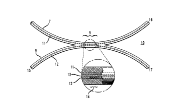
An optical filter comprises a plurality of optical fibers having a coupling
region where the axially extending cores are closely spaced within a common
cladding. The coupling region includes a long period grating for selectively shifting
light of selected wavelengths from guided modes into non-guided modes. These
non-guided modes are picked up by an adjacent core and light of the selected
wavelengths is thus shifted from one core to another. The result is an optical filter
particularly useful as a demultiplexer or a tapping device. In one embodiment the
grating is formed in one of the cores. In an alternative embodiment, it is formed in
the common cladding.


French Abstract

L'invention est un filtre optique comportant une pluralité de fibres optiques ayant une région de couplage où les âmes axiales sont rapprochées les unes des autres et entourées d'une gaine commune. La région de couplage comprend un réseau à période longue servant à faire passer la lumière à certaines longueurs d'onde particulières d'un mode de propagation guidée à un mode de propagation non guidée. La lumière en propagation non guidée est recueillie par une âme adjacente et la lumière aux longueurs d'onde particulières sélectionnées passe donc d'une âme à une autre. On obtient ainsi un filtre optique particulièrement utile comme démultiplexeur ou dispositif de dérivation. Dans l'une des concrétisations de l'invention, le réseau est formé dans l'une des âmes. Dans une autre concrétisation, il est formé dans la gaine commune.

Claims

Note: Claims are shown in the official language in which they were submitted.


Claims:

1. An optical filtering device comprising:
a plurality of optical waveguiding cores extending side-by-side in a common
cladding, and
a grating for shifting light in a guided mode in one of said cores to a
non-guided mode, said grating comprising a plurality of index perturbations spaced apart
by a periodic distance .DELTA., where 50 µm ~ .DELTA. < 1500 µm.

2. The device according to claim 1 wherein said grating is in one of said
cores.

3. The device according to claim 1 wherein said grating is in said common
cladding.

4. The device according to claim 1 wherein said cores are spaced apart by
less than 10 mean core diameters.

5. The device according to claim 1 wherein said index perturbations have
a width w, where 1/5 .DELTA. ~w ~4/5 .DELTA..

6. The device according to claim 1 wherein said pair of optical cores in a
common cladding comprises a pair of optical fibers fused together.

Description

Note: Descriptions are shown in the official language in which they were submitted.


OPTICAL TAPPING FILTERS EMPLOYING
- LONG PERIOD GRATINGS
Field of the Invention
This invention relates to optical communications devices and, in particular to
5 optical filters employing long period gratings.
Back~round of the Invention
Optical fiber communications systems are becoming increasingly important in
the high speed tr~n~mi~.~ion of large amounts of information. A typical fiber
communications systems comprises a source of optical input signals, a length of
10 optical fiber coupled to the source, and a receiver for optical signals coupled to the
fiber. In essence, an optical fiber is a small diameter waveguide characterized by a core
with a first index of refraction surrounded by a cladding having a second (lower) index
of refraction. Light rays which impinge upon the core at an angle less than a critical
acceptance angle undergo total internal reflection within the fiber core. These rays are
15 transmitted with minimum attenuation in guided modes along the axis of the fiber.
Optical filters are used for shaping the spectral features of transmitted optical
pulses, and multiplexers are used for transmitting a multiplicity of different signals at
different wavelengths. The present invention relates to devices which can be used as
filters and as demultiplexers to separate multiplexed signals in optical communications
20 systems.
Summar,v of the Invention
An optical fiber comprises a plurality of optical fibers having a coupling region
where the axially extending cores are closely spaced within a common cl~(l(1ing. The
coupling region includes a long period grating for selectively shifting light of selected
25 wavelengths from guided modes into non-guided modes. These non-guided modes are
picked up by an adjacent core and light of the selected wavelengths is thus shifted from
one core to another. The result is an optical filter particularly useful as a demultiplexer
or a tapping device. In one embodiment the grating is formed in one of the cores. In an
alternative embodiment, it is formed in the common cl~(l(lin~.
In accordance with one aspect of the present invention there is provided an
optical filtering device comprising: a plurality of optical waveguiding cores extending
side-by-side in a common cl~l(1ing, and a grating for shifting light in a guided mode in
one of said cores to a non-guided mode, said grating comprising a plurality of index
perturbations spaced apart by a periodic distance ~, where 50 ~Lm ~ 1500 ~lm.
35 Brief Description of the Drawin~s

2 1 68902


FIG. 1 is a schematic view of an optical filter in accordance with one
embodiment of the invention;
FIGs. 2, 3 and 4 are qualitative spectral diagrams of an optical pulse at
various locations in the device of FIG. l;
FIG. 5 is a graphical plot of center wavelength versus period useful in
making the device of FIG. 1; and
FIG. 6 is a second embodiment of a filter in accordance with the
invention.
Detailed D~,;~ n
Referring to the drawings, FIG. 1 is a schematic cross section of a first
embodiment of an optical filtering device 10 comprising a plurality of optical
fibers 7 and 8 joined along a coupling region 9. Within the coupling region, theaxially extending waveguiding cores 11 and 12 are closely spaced within a commoncladding 13. Preferred center-to-center spacing between the cores is less than 10 core
15 diameters (or less than 10 mean core diameters if the cores have unequal diameters).
One of the cores, here core 12, includes a long period grating 14 for selectively
shifting light of selected wavelengths from guided modes into non-guided modes.
Because of the coupling between the two cores, much of the light shifted from
guided modes in core 12 is coupled to core 11 where it is absorbed into guided
20 modes. Advantageously, the device is provided with at least three ports 15, 16 and
17. In typical operation, optical input pulses will enter the device via port lS which
has a core region continuous with grating core 12. One output can be taken from
port 16 which is continuous with core 11 and another can be taken from port 17
which is continuous with core 12. While a two-core device is shown in FIG. 1, it25 will be appreciated that similar devices can be made employing three or more cores.
The long period grating 14 comprises a plurality of index pe,lull,ations
of width w spaced apart by a periodic distance A where, typically, 50 llm < A S
1500 ~lm. Advantageously, llSA<w<415A and preferably w=l/2A. The
perturbations are formed within the glass core of the fiber and preferably form an
30 angle 0(2~~90~) with the longitudinal axis of the fiber. The fiber is designed to
transmit broad band light of wavelength centered about ~O.
The spacing A of the pe,lu~bations is chosen to shift transmitted light in
the region of a selected wavelength ~p from the guided mode into a non-guided
mode, thereby reducing in core 12 the intensity of light centered about ~p. In
35 contrast with conventional short period gratings which reflect light, these long period
devices remove the light without reflection by converting it from a guided mode to a

2 1 6g902


non-guided mode. A substantial portion of the non-guided light couples into core 11
where it excites guided modes, producing in 11 a narrow pulse of light centered
about ~p.
FIGs. 2, 3 and 4 illustrate the operation of the device. FIG. 2 shows the
5 spectrum of a relative broad pulse of light centered about ~O entering core 12 via
port 15. FIG. 3 shows the spectrum of the relatively narrow pulse of light centered
about ~p which is coupled from core 12 to core 11 and exits via port 16. FIG. 4
shows the spectrum of the pulse on core 12 at port 17 after the light has passedthrough the long period grating 14. The pulse is ~limini~hed in a region near ~p.
FIG. S is a graph useful in designing the long period grating 14.
Specifically, FIG. 5 plots for a communications optical fiber with core ~=.3% and
core diameter of 8~Lm the periodic spacing A for shifting to an unguided mode, light
centered about a wavelength ~p. Thus, for example, to make a device for shiftinglight centered around 1540 nm, one chooses a spacing of about 760 llm. Similar
15 curves can be empirically determined for other specific fibers.
Preferably the device is made by fusing together in the coupling region,
two separate optical fibers. One fiber can have a core, such as germanosilicate glass,
which is sensitive to UV radiation, and the other can have a core, such as aluminum
or phosphorous doped silica, which is in.cen~itive to UV radiation. The cl~d~ing~ can
be fused, as by the application of heat, and UV sensitivity can be enhanced by
diffusing H 2 or D 2 into the glass. Alternatively, a single fiber having a plurality of
cores and a common cladding can be drawn from preform cont~ining a
corresponding plurality of core rods.
The long period grating can be written by exposing the fused region to
U V radiation, e.g. 248 nm radiation from a KrF laser, through a slit or a mask. If a
slit is used, the fiber is moved to successive exposure sites. The preferred exposure
dosage for each slit is on the order of 1000 pulses of > 100mJ/cm2 fluence/pulse,
and the number of index perturbations is in the range 10-100.
FIG. 6 illustrates the coupling region of an altemative embodiment of an
30 optical filtering device similar to FIG. l wherein the long period grating 60 is formed
in the cladding common to a plurality of cores rather than in one of the cores. With
this arrangement, the cores are advantageously of different diameter or different
index so that light at the mid-band ~p for the grating is preferentially coupled into
one of the cores.

,, 21~q~2

- 4 -
A convenient way to make the FIG. 6 device is to provide fibers with
W sensitive cladding (e.g. germanosilicate glass) and UV incen~itive cores (e.g.aluminum or phosphorous doped silicates). The grating can be written as described
above, but will form only in the UV sensitive cladding.

Representative Drawing
A single figure which represents the drawing illustrating the invention.
Administrative Status

For a clearer understanding of the status of the application/patent presented on this page, the site Disclaimer , as well as the definitions for Patent , Administrative Status , Maintenance Fee  and Payment History  should be consulted.

Administrative Status

Title Date
Forecasted Issue Date 1999-03-30
(22) Filed 1996-02-06
Examination Requested 1996-02-06
(41) Open to Public Inspection 1996-08-25
(45) Issued 1999-03-30
Deemed Expired 2003-02-06

Abandonment History

There is no abandonment history.

Payment History

Fee Type Anniversary Year Due Date Amount Paid Paid Date
Application Fee $0.00 1996-02-06
Registration of a document - section 124 $0.00 1996-08-01
Maintenance Fee - Application - New Act 2 1998-02-06 $100.00 1998-01-06
Final Fee $300.00 1998-12-15
Maintenance Fee - Application - New Act 3 1999-02-08 $100.00 1998-12-30
Maintenance Fee - Patent - New Act 4 2000-02-07 $100.00 1999-12-20
Maintenance Fee - Patent - New Act 5 2001-02-06 $150.00 2000-12-14
Owners on Record

Note: Records showing the ownership history in alphabetical order.

Current Owners on Record
AT&T IPM CORP.
Past Owners on Record
VENGSARKAR, ASHISH MADHUKAR
WALKER, KENNETH LEE
Past Owners that do not appear in the "Owners on Record" listing will appear in other documentation within the application.
Documents

To view selected files, please enter reCAPTCHA code :


To view images, click a link in the Document Description column. To download the documents, select one or more checkboxes in the first column and then click the "Download Selected in PDF format (Zip Archive)" or the "Download Selected as Single PDF" button.

List of published and non-published patent-specific documents on the CPD .

If you have any difficulty accessing content, you can call the Client Service Centre at 1-866-997-1936 or send them an e-mail at CIPO Client Service Centre.


Document
Description 
Date
(yyyy-mm-dd) 
Number of pages   Size of Image (KB) 
Representative Drawing 1998-06-10 1 13
Cover Page 1999-03-22 1 50
Cover Page 1996-05-29 1 18
Abstract 1996-05-29 1 17
Description 1996-05-29 4 163
Claims 1996-05-29 1 20
Drawings 1996-05-29 2 33
Claims 1998-07-08 1 22
Description 1998-07-08 4 176
Representative Drawing 1999-03-22 1 8
Correspondence 2003-01-28 1 21
Correspondence 2003-02-13 1 13
Correspondence 1998-12-15 1 36
Prosecution Correspondence 1998-06-18 2 54
Examiner Requisition 1998-03-20 2 79
Prosecution Correspondence 1996-02-06 5 212