Note: Descriptions are shown in the official language in which they were submitted.
CA 02168949 2003-12-17
-1 -
DROPLET DEPOSITION APPARATUS AND METHOD OF
MANUFACTURE
The present invention relates to droplet deposition apparatus and
especially to ink jet printheads made of piezo-electric ceramic. , In
particular
it relates to methods for bonding such printheads during assembly. The
invention finds particular applications in the manufacture of printheads
employing shear mode wall actuators.
For example, in US-A-5,003,679 (EP-B-0 277 703) there is
disclosed a method of making multi-channel pulsed droplet deposition
apparatus comprising the steps of forming a base with one or more layers of
piezo-electric material, forming a multiplicity of parallel grooves in said
base
which extend through said layer or layers of piezo-electric material to afford
walls of said material between successive channels, locating electrodes in
relation to said walls so that an electric field can be applied to effect
shear
mode displacement of said walls transversely to said channels and securing
a top wall to the walls to close said liquid channels.
An alternative example of piezo-electric shear mode ink jet
printheads is provided in US-A-5,016,028 (EP-B-0 364 136),
A particular feature of a preferred embodiment of the latter reference
is that for satisfactory actuation of the actuator walls between channels, the
compliance ratio of the bond layer which secures the top wall to the actuator
wails (the compliance ratio is hE/He where h is the thickness of the bond
layer, a is the modulus of elastic of the layer, H is the height of the walls
and E is the modulus of elasticity of the walls) is less that 1 and preferably
less that 0.1. For example, if H = 440~Cm E = 110 GPa and a = SGPa, the
latter value stipulates that approximately the bond layer thickness h < 2~cm.
Whilst a variety of techniques exist for bonding piezo-electric ceramic
material to other ceramics onto glass and other substrate materials used in
ink jet printhead manufacture, the most flexible and convenient technique is
often adhesive bonding. The term adhesive is intended to include all
suitable glues and cements. However, real difficulties are encountered in
WO 95104658 PCT/GB94/01747
~'~b~~4~ -2-
providing a uniform adhesive bond layer of thickness 2um or less.
It is an object of this invention to overcome some or all of these
difficulties in providing an improved method of manufacturing multi-channel
pulsed droplet deposition apparatus.
Accordingly, the present invention consists in one aspect in a method
of making multi-channel pulsed droplet deposition apparatus comprising the
steps in any order of bonding together a stack of layers comprising at least
one layer of piezo-electric material and a cover layer; forming a multiplicity
of parallel grooves in said stack which extend at least partly through said
layer of piezo-electric material to afford walls of said material between
successive droplet liquid channels, said channels being closed by said cover
layer; and locating electrodes in relation to said walls so that an electric
field
can be applied to effect shear mode displacement of said walls transversely
to said channels; characterised in that the bonding together of two of said
layers comprises the steps of preparing respective mating surfaces of said
layers to reduce the surface roughness to the order of 2~rm or less; applying
an excess of adhesive and with the mating surfaces in register applying
pressure and allowing adhesive to flow in the bonding plane until surface
extremities of the respective mating surfaces come into substantially direct
contact to produce a bond layer of mean thickness 2Nm or less.
By suitably controlled lapping or grinding, it is possible to control the
roughness of each of the mating faces so that when they are brought
together in contact, in the absence of the bond layer, the surfaces conform
so that mean separation between the faces is 2~cm or less. However, when
a bond layer of a suitable glue is applied to the surfaces and the surfaces
are brought together in contact under pressure, the bond layer builds up
hydrostatic pressure inhibiting intimate contact of the mating surfaces and
resulting in excessive bond compliance.
Attempts to reduce the problem of hydrostatic pressure by reducing
the amount of adhesive which is applied, run the risk of leaving certain
regions improperly bonded. The fine scale of the walls and the criticality of
the bond in the correct operation of the completed apparatus, compound this
WO 95/04658 ~ 1 ~ ~ ~ ~ PCT/GB94/01747
-3-
problem. In this aspect of the present invention, however, an excess of
adhesive is used and pressure is applied until surface extremities of the
mating surfaces come into substantially direct contact, with the adhesive
filling the interstices. The distance which excess adhesive is required to
travel in the bonding place is preferably kept uniform over the entire
interface suitably to a maximum of 100~Cm. Where one of the bonding
surfaces is divided by the parallel grooves into strips of no more than this
width, excess adhesive is permitted to flow into the grooves. It is found that
the presence of excess adhesive in the channels of the completed apparatus
has no material effect on performance. In other cases, adhesive flow
formations are provided at the bond interface to accommodate excess
adhesive and to maintain the maximum flow distance.
The invention will now be described by way of example by reference
to the attached diagrams in which:-
Figure 1 illustrates an exploded view in perspective of one form of ink
jet printhead incorporating shear mode wall actuators.
Figure 2 illustrates a section view normal to the ink channels of the
printheads illustrated in Figure 1 after assembly.
Figure 3 illustrates a detail of the printhead of Figure 2 in which one
example is shown of the problems to which the invention is addressed.
Figure 4 illustrates one embodiment of the invention which provides ~a
solution to the problem of Figure 3.
Figure 5 illustrates an alternative embodiment of the invention which
provides a second solution.
Figures 6 and 7 show a laminate wafer comprising three ceramic
layers suitable for the manufacture of ink jet printheads incorporating shear
mode wail actuators of the chevron design type.
Figure 8 illustrates how the invention is applied to the formation of the
laminate wafer of Figures 6 and 7 to reduce the bond compliance between
the ceramic layers.
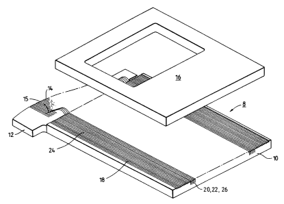
Figure 1 shows an exploded view in perspective of an ink jet
printhead 8 incorporating piezo-electric wall actuators operating in shear
WO 95/04658 PCT/GB94101747
z1~~~4~
-4-
mode. It comprises a base 10 of piezo-electric material mounted on a
circuit board 12 of which only a section showing connection tracks 14 is
shown. A cover 16, which as will be described later is bonded during
assembly to the base 10, is shown above its assembled location. For
clarity, the nozzle plate is omitted in the drawings.
A multiplicity of parallel grooves 18 are formed in the base 10
extending into the layer of piezo-electric material. The grooves 18 are
formed as described in the above reference US-A 5,016,028
(EP-B-0 364 136). The base has a forward part in which the grooves are
comparatively deep to provide ink channels 20 separated by opposing
actuator walls 22. The grooves rearwardly of the forward part are
comparatively shallow to provide locations for connection tracks 24. After
forming the grooves 18, metallised plating is deposited in the forward part
providing electrodes 26 on the opposing faces of the ink channels 20. The
plating in the forward part extends over approximately one half of the
channel height and in the rearward part provides the connection tracks 24
connected to the electrodes in each channel 20. The tops of the walls
separating the grooves are kept free of plating metal so that the track 24
and the electrode 26 in each channel are electrically isolated from other
channels.
After the deposition of metallised plating and coating of the base
part 10 with a passivant layer for the electrical isolation from ink of the
electrode parts, the base 10 is mounted as shown in Figure 1 on the circuit
board 12 and bonded wire connections 15 are made connecting the
connection tracks 24 on the base 10 to the connection tracks 14 on the
circuit board 12.
Assembly of the cover 16 by bonding the cover to the base 10 is now
described by reference to Figures 2 to 5. Figure 2 shows the
cover 16 secured to the tops of the walls 22 in the base 10 by a bond
layer 28. A suitable material for bonding is an epoxy resin mix which
becomes highly polymerized after curing such as Epotek 353ND.
Advantageously, the resin mix may incorporate a silica flour such as
WO 95/04658 ~ ~ ~ ~ PCT/GB94/01747
-5-
Degussa Aerosil 8202 to stiffen the bond after curing.
As indicated in the above reference the bond layer 28 is preferably
formed with a low compliance so that the actuator walls 22, where they are
secured to the cover 16, are substantially inhibited from rotation and shear.
The compliance ratio of the bond layer 28,where it secures the actuator
wails to the cover (the compliance ratio is hE/He where h is the thickness of
the bond layer, a is the modulus of elasticity of the layer, H is the height
of
the actuator walls and E is the modulus of elasticity of the walls) should be
less than 1 and preferably less than 0.1.
By suitably specified lapping or grinding, the roughness of the mating
surfaces of the base 10 at the tops of the walls 22 and the
cover 16 is controlled, so that when they are brought together under bonding
pressure but in the absence of a bond layer, the faces conform so that the
mean separation of the surfaces is 2~rm or less. A typical bond pressure in
the context of this invention is around 50 atmospheres. When the space
separating the faces is filled with the bonding material, which is cured, the
bond compliance is then a result of the elastic characteristics of the glue
layer. It is generally recognised that very little additional stiffness is
contributed by the direct contact between the surface asperities. The
problem is, however, that the application of an adhesive layer may result in
a bond layer of thickness above the desired minimum.
To ensure complete coverage of the surfaces by glue, it is cesirable
to apply an excess, as opposed to too thin a layer. When the surfaces are
brought together in contact under pressure, the excess glue in Fegions such
as the tops of the walls 22 is found to flow within the surface pores, so that
the surfaces come into contact in the surface asperities thereof with a mean
separation substantially the same as is obtained in the absence of the bond
layer. Excess glue corresponding to a layer 3-S~Cm thick spreads into of the
adjacent channels and harmlessly coats the channel surfaces.
The problem indicated above arises, for example, when the surfaces
between the cover 16 and the lands 31 on outer walls 30 of the printhead
are brought together under pressure. The bond layer material between
WO 95/04658 ~ ~ ~ PCT/GB94/01747
-6-
these faces is not readily squeezed out but builds up a hydrostatic pressure,
inhibiting the close contact of the mating surfaces. This is partly due to the
fact that (for a viscous material) the time to squeeze out the excess layer of
bond material varies as the third power of the distance over which the
excess material is required to flow. For example, if the outer wall 30 is ten
times wider than the actuator walls 22, the required time is one thousand
times greater. In addition, the glue may be non-Newtonian, so that the time
is even more extended. The required time for the surface to make contact if
that result is obtained is not usually available in a mass production process.
Figure 3 illustrates the effects that arise due to the excess glue under the
outer wall 30, where not only is the bond layer between the rigid inactive
outer wall 30 seen to be thick, but also - due to local flexural rigidity of
the
cover - the glue film remains thick over a group of actuator walls at the
edge of the printhead 10 with the result that the bond compliance at the top
of the walls is too great. Such a printhead will therefore have walls that do
not pass the test specified in US-A-4,973,981 (EP-B-0 376 532) or another
equivalent test and may be rejected in manufacture.
The problem of forming a precisely metered thin glue bond layer over
an extended area, such as over the outer walls 30, may be overcome as
illustrated in Figure 4 where a number of shallow grooves 32 are formed on
the top of the outer walls 30. These may be formed at the same time as the
formation of the channels 20 in the forward part, and may conveniently be
formed to a similar depth as the grooves in the rearward part of the wall 10:
advantageously they may be of the same width and spacing as the channel
grooves 18. Although two such grooves are illustrated, a greater number
such as 10, 20 or more grooves may be provided depending on the outer
wall width.
The intention is that the maximum distance which excess adhesive
has to travel in the bonding plane over the marginal land 31 is approximately
the same distance as over the bulk of the base region, that is to say the
thickness of one wall 22.
When excess glue is provided, for example by screen printing of glue
~~~~~4~
WO 95/04658 - PCT/GB94/01747
-7-
on the surface of the base wall 10, and the cover 16 is brought into contact
with the base wall under pressure, the grooves 32 formed in the outer
wall 30 provide a channel into which excess glue may flow, so that intimate
conformity in the region of the outer wall 30 is obtained as readily as on the
tops of the actuator walls. Further, if excess glue is provided in the
quantity
to X11 the grooves 32, it can more readily flow along the grooves and escape,
avoiding build-up of hydrostatic pressure between the mating parts. It is
further more easy to regulate the application of a quantity of glue in excess
to ensure successful bond formation, without the deleterious compliance
effects to the active walls.
An alternative embodiment is illustrated in Figure 5 in which the
grooves, in contrast to being formed in the base wall as described above,
are formed in the cover 16. When the cover 16 is made of the same
material and by the same process as is the base 10, the grooves are
preferably formed in the cover by the same process that employed for
manufacture of the base. It may alternatively be preferable to make the
cover of different materials or by a different process. For example the cover
may be a ceramic formed by powder pressing and firing, it being important
to select a material for this process whose thermal expansion coefficient
substantially matches that of the piezo-electric ceramic from which the base
is made. In that case the grooves in the cover 16 may be formed by
indenting the press faces during the pressing operation. The thinness of the
bond layer means that the need for matching the thermal expansion
coefficients of the materials to be bonded, is particularly acute. allatching
to
at least 1 ppm is preferred.
The formation of indented features 32 in the cover 16 also places less
constraints on the pattern of indentation employed in the region facing the
outer wall of the base part. Instead of grooves, indented pits, or
crosshatching or any suitable stipple pattern may be adopted which provides
adhesive flow formations. It is important that the tops of the patterned
regions are ground or lapped or otherwise formed to maintain the specified
surface flatness, and that the edge adjacent the outermost channel provides
CA 02168949 2003-12-17
-
a continuous bonded seal for ink in the outermost channel.
The problem of forming a precisely metered thin glue layer over an
extended area similarly arises in forming a bonded piezo-electric laminate
wafer 40 as described by reference to Figure 6 and Figure 7. The
laminate 40 comprises three ceramic layers which are bonded together. The
base layer 42 is an insulating ceramic, which in one form is
non-piezo-electric. To the base layer are bonded two poled piezo-electric
ceramic layers 44 and 46, the poling directions being in anti-parallel as
indicated in figure 6 in the left hand scrap section.
The laminate is useable for manufacture of ink jet array printheads
which employ shear mode wall actuators, of "chevron design" type as
disclosed in US-A-5,003,679 and US-A-4,887,568 (EP-B-0 277 703) and
in US-A-4,887,100 (EP-B-0 278 590). The laminate is cut through the
piezo-electric layers 42 and 44 forming a multiplicity of parallel grooves i 8
providing ink channels 20 separated by actuator walls 22. Metallised plating
is deposited on the opposing faces of the ink channels as shown in the right
hand scrap section, where it extends the full height of the channel walls
providing actuation electrodes. The walls are coated with a passivant layer
for electrical isolation of the electrode part from ink, and a cover is
secured
to the tap of the walls. Walls of this type being active in both the top and
bottom halves are advantageous because they are able to be .operated with
a lower voltage. Such aspects are described in more detail in the above
prior art,
The laminate wafer illustrated in Figure 7 is formed of three bonded
layers as described by reference to Figure 6 and is of area sufficiently great
to provide a muftiplicity~ of ink jet printheads. Twenty are illustrated, but
the
method of manufacture below is suitable for wafers accommodating any
suitable large number of printheads for mass manufacture. Horizontal and
vertical lines 47 and 48 show where individual actuators are diced and
parted.
As previously indicated, it is important that the bond layers between
the ceramic layers 42, 44 and 46 are thin and have a low compliance. This
WO 95/04658 ~ ~ ~ ~ ~ ~ ~ PCT/GB94/01747
_g_
is necessary to ensure that the wall actuators 22, where the layers are
bonded one to another, are substantially inhibited from elastic rotation and
shear, and that, when subjected to actuation voltages, pressure is efficiently
generated in the ink inside the channels in accordance with the voltage
actuation pattern.
Suitably controlled surface roughness of the mating surfaces of the
ceramic layers 42, 44 and 46 may be obtained by lapping or grinding so that
when they are brought together in contact under pressure they touch at the
surface asperities and conform with a mean surface separation of 2um or
less. It is consequently the thickness of the intermediate bond layer
between the ceramic layers that governs the bond compliance.
The surface roughness of the mating surfaces can be measured with
Talysurf equipment providing a value RA which is preferably less than 2um.
It will be recognised that opposing surfaces having each a value RA of, for
example, ,~2um are likely to produce, when the surface extremities are in
contact, a surface layer of mean thickness approximately 2um.
The formation of suitably thin bond layers is achieved as illustrated in
Figure 8, which is a section of the laminate of Figures 6 and 7. It is
accomplished by providing grooves 50 in one or other of the mating surfaces
between each of the ceramic layers parallel to and in the locations of the
channels 20. The grooves are located in manufacture by using the edges of
the wafer to provide reference edges and are preferably cut narrower than
the channels. In regions of a printhead where there are no ink channels,
grooves 50 are nevertheless also formed. _
When the ceramic layers are coated with glue which is applied in
excess and the layers are brought into contact under pressure, the excess
glue can flow into and along the grooves so that the tendency to develop
substantial hydrostatic pressure in the glue layer during assembly and
bonding is avoided and intimate conformity of the ceramic layers is attained.
If flow of glue along the grooves 50 in the channel direction is insufficient
to
avoid the hydrostatic pressure preventing conformity of the layers, cross
grooves (not shown) may also be formed in the locations of the part lines 47
WO 95/04658 PCTIGB94101747
z1~~~4~ -10-
or 48, to provide secondary drainage. The volume of the primary
grooves 50 in the channel direction however will normally be sufficient to
accommodate excess glue and allow conformity of the ceramic layers.
Following bonding of the ceramic layers under pressure, the laminate
wafer 40 is cut through the piezo-electric layers 46 and 44 forming
grooves 18 as illustrated in Figures 6, providing ink channels 20 separated
by the actuator walls 22. The locations of the grooves 50 is shown in
relation to the ink channels 20 in the scrap section in Figure 8 on the right
as outline grooves shown as dotted lines representing the location of some
of the grooves 50 prior to removal of the channel material. The grooves 18
are formed by edge reference of the wafer approximately at the same
centres as the grooves 50 so removing the material forming as well as the
excess glue in those grooves. The bond compliance of the bond layers
forming the wall actuator obtained using the above process is found to be
reduced so that the bond compliance ratio satisfies the requirement
(hElHe) < 0.1 as may be confirmed by resonance tests of the type described
in the patent reference US-A-4,973,981 (EP-B-0 376 532).