Note: Descriptions are shown in the official language in which they were submitted.
2 i 690
94-mCON 424 (AU)
CAPACITIVE SWITCHING ASSEMBLY
BACKGROUND OF THE INVENTION
The present invention relates to switches of the type employed for switching
fractional ampere current where it is desired to have a push-to-actuate type
of operation.
Switches of this type are desirable where low cost, compact size and minimal
protrusion from
a panel are desired.
Heretofore known low current switches have employed various techniques, one of
which has been push-to-actuate switches which employ over-center or toggle
spring
mechanisms to move the contacts of the switch in response to user movement of
the actuator.
Such switches have proven to be widely used because of their positive making
and breaking.
characteristics, but are relatively costly in high volume mass production
because of the
numerous discrete parts and costly noble metal contacts required for
performing the
switching operation and to minimize arcing upon breaking. Where fractional or
subfractional
ampere current is being switched, the need for noble metal or separate
contacts for switching
the current and preventing arcing is eliminated. Therefore, it has been
desired to provide a
simpler yet reliable and lower cost switch for low current switching element
with fewer parts.
Heretofore, capacitance change type switching has been used for smooth panel
switches where the user touches a laminant on the panel which effects a change
in
capacitance as between two plates which is then detected by appropriate
circuitry and
discerned as a switching operation. However, known capacitance switching has
not provided
2 0 for significant movement or tactilely discernible switching action to give
positive feedback to
the user that the switching has occurred. It has therefore been desired to
provide a low
current switching mechanism which is minimum in manufacturing cost and which
provides
the movement and tactilely discernible indication of movement similar to
switching that of a
mechanical contact type switch without the need for such contacts.
-
CA 02169001 1999-09-21
94-mCON 424 (AU)
SUMMARY OF THE INVENTION
The present invention provides a push button actuated low-current switch which
provides a tactically discernible indication of switch actuation by movement
and increasing
force and performs a switching operation by the significant detection of
change in
capacitance of a pair of series connected capacitors.
The present invention also provides a switching operation by user
compression of a resilient conductive pad in contact with dielectric coating
on the surface on
the pair of spaced coplanar plates and effects a change in capacitance of a
pair of series
capacitors by resilient compression of the pad.
The invention also provides capacitance change switching by
moving a conductive elastomeric member into contact with dielectric material
on the surface
of a pair of spaced coplanar plates and compressing the elastomeric material
to effect a
change in capacitance which is detected for switching purposes.
The present invention employs a pair of relatively thin conductive plates or
film on
the surface of a non-conductive substrate with a coating of dielectric
material over the
exposed faces of the plates. A user moveable actuator or direct contact
effects compression
of a resilient conductive pad or disc which is in contact with the dielectric
material and
continued movement of the actuator effects compression of the elastomeric disc
which brings
about a change of capacitance of the plates which is detectable for effecting
a switching
2 0 function. In one embodiment the resilient pad is conductive elastomeric
material and in
another embodiment the pad is non-conductive elastomer with a thin conductive
foil on the
surface thereof.
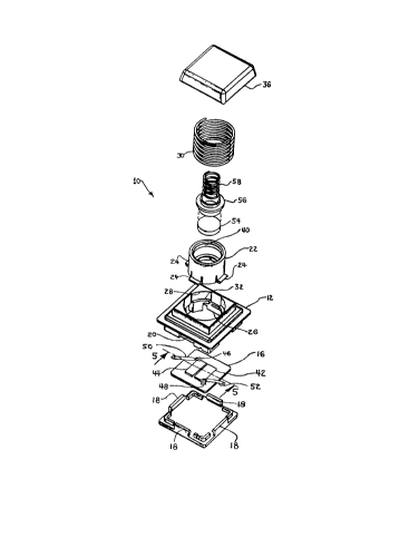
FIG. 1 is an exploded view of the switch assembly of the present invention;
2 5 . FIG. 2 is a top view of the assembled switch of FIG. l;
FIG. 3 is a section view taken along section indicating lines 3-3 of FIG. 2;
FIG. 4 is a section view taken along section indicating lines 4-4 of FIG. 2;
FIG. 5 is an enlarged view taken along section indicating lines 5-5 of FIG. 1;
-2-
2169001
94-mCON 424 (AU)
FIG. 6 is a graphical plot of values of capacitance as a function of pad
compression
for the embodiment of FIG. 5.
FIG. 7 is another embodiment of the invention; and,
FIG. 8 is a graph similar to FIG. 6 for the embodiment of FIG. 7.
s DETAILED DESCRIPTION
Referring to the drawings, the switch assembly indicated generally at 10 has a
housing means comprising a main frame 12 and a cover 14 which is attached,
preferably
snap-locked, to the frame 12. A substrate or base 16 is sandwiched between the
main frame
12 and cover 14 and secured therebetween. The cover 14 preferably has a
plurality of tabs or
projections 18 disposed thereabout which engage correspondingly disposed
grooves 20
provided about the periphery of the lower portion of frame 12 in snap-locking
engagement.
Frame 12 has attached thereto a preferably hollow cylindrical tower portion 22
which
is attached to the mainframe 12 by snap-locking engagement of a plurality of
lugs 24
disposed about the periphery of the tower 22 at or adjacent one end thereof.
The tower 22 is
nested in the frame 12 such that the lugs 24 engage an undercut or shoulder 26
provided
therein. The tower portion 22 is slidably received in the counter-bore 28
formed in the frame
12 and a spring 30 is nested about the outer periphery of the tower 22. One
end of the spring
30 is registered against an annular shoulder 32 provided in the bore 28.
The opposite end of spring 30 is registered against the under surface 34 of a
push
2 0 button 36 received over the end of the tower 22. Push button 36 has an
annular registration
portion 38 depending from the undersurface which is snap-lock engaged with a
groove 40
formed in the inner periphery of the tower 22 for retaining the push button
thereon.
Substrate or base 16 has a pair of plates 42,44 formed of conductive material
and
which may be thin film conductive material disposed in spaced coplanar
arrangement, each
2 5 having a tab or connector portion respectively 46,48 formed thereon for
attachment of
electrical leads thereto. If desired electrical connections may be made by
soldering leads to
the tabs 46,48 as denoted respectively by reference numerals 50,52 in FIG. 1.
The plates 42,44 are secured to the base 16 by any suitable adhesive or
bonding
arrangement. In the presently preferred practice of the invention, the
substrate or base is
-3-
'~ i ~9uU
94-mCON 424 (AU)
formed of a refractory aluminum oxide material. The plates 42,44 are
subsequently coated
with a dielectric material and the subassembly thereof is fired at a
temperature of 930°C to
cure the substrate plates and the dielectric material. In the presently
preferred practice the
electrode material is screened on the substrate and the dielectric is screened
over the
conductive material.
Referring to FIGS. 1 and 5, the substrate 16 has the plates 42,44 formed
thereon
preferably by screening of conductive ink formed of a mixture of palladium and
silver; and,
superposed thereon is a preferably screened layer of dielectric material
denoted by reference
numeral 60. In the present practice of the invention a mixture of
ferroelectric and glass
material has been found satisfactory for the dielectric and, in particular a
material bearing
manufacturer's design "D-4117" and obtained from Electroscience Laboratories,
Inc., 416
East Church Road, King of Prussia, Pennsylvania 19406, having a thickness in
the range 40-
60 microns (10'~ meters). In the presently preferred practice, the conductive
layers forming
plates 42, 44 or 11.5 plus or minus 1.5 microns (10'~ meters).
Referring to FIGS. 1, 3, 4 and 5, a switching member 54 or pad having a
generally
disc-shaped configuration and formed of resiliently deforrnable material is
attached to the
undersurface of a plunger member 56, preferably by adhesive bonding. The
plunger is
slidably received in the inner surface of the tower 22 and guided for movement
therein. The
plunger 56 is biased in a direction for movement towards the base 16 by one
end of a spring
2 0 58 which has its opposite end registered against the undersurface of push
button 36. In the
present practice, elastomeric disc 54 of the embodiment shown in FIG. 5 is
formed of silicon
rubber interspersed with carbon to provide the desired conductivity and has a
barometer of 60
measured on the shore "A" scale. A satisfactory material may be obtained from
Stockwell
Rubber Co., 4749 Tolbut Street, Philadelphia, Pennsylvania 19136.
Referring to FIGS. 1 and 5, upon user movement of push button 36 toward the
substrate 16, spring 58 is compressed pushing piston 56 and disc 54 toward the
substrate until
the disc 54 contacts the dielectric along the interface denoted D° in
FIG. 5. Continued
pressure on the push button by the user causes further compression of the
springs 58,30 and
effects some compression of the elastomeric material of disc 54.
-4-
i r-~
94-mCON 424 (AU)
Referring to FIG. 6, the capacitance measured between leads 50, 52 is plotted
as a
function of the compression of the elastomer after contact along line Do. It
will be seen from
FIG. 6 that approximately 0.25 millimeters compression of the disc is required
before a
significant increase in capacitance occurs; and, an additional 0.15
millimeters compression
provides orders of magnitude increase in capacitance which may be readily
detected to
provide a switching function.
Referring to FIGS. 7 and 8, another embodiment of the invention is illustrated
wherein the elastomeric disc 54' is formed of elastomeric material having no
conductivity;
and, a conductive layer of metal foil 55 is cemented to the surface thereof to
provide the
completion of the two capacitors upon contact of the foil with the dielectric
material 60 of
plates 42, 44. In the present practice of the invention the elastomeric disc
54' is made of very
low elastomeric sponge material having a relatively low durometer and has a
thickness of 3.5
millimeters. The conductive foil 55 has a thickness of 0.06 millimeters and is
preferably of
aluminum material.
Referring to FIG. 8, which is a graph similar to FIG. 6, it will be seen that
for the
embodiment of FIG. 7, the capacitance change occurs significantly upon initial
contact of the
metal foil 55 with the dielectric 60 and thereafter a compression of only 0.25
millimeters
gives a significant fi~rther increase; and, the capacitance increases tenfold
upon a
compression of the sponge material of the disc 54' by an amount of 2.75
millimeters.
2 0 The present invention thus provides a push-to-actuate switch assembly
employing a
resilient pad and conductive material pressed against the surface of
dielectric material
superposed over spaced coplanar plates to form a pair of series connected
capacitors and,
upon contact of the resilient pad with the dielectric material. Compression of
the pad
dramatically increases the capacitance in a manner which is readily detectable
for effecting a
switching function. In one embodiment the resilient pad is formed of
conductive elastomer
and in a second embodiment a nonconductive elastomer is coated with a thin
conductive
metal foil.
Although the invention has been illustrated with an actuator which moves the
pad
54,54' from a position initially spaced from the dielectric coating over the
plates 42,44, it will
3 0 be understood that the actuator mechanism may be modified such that the
pad 54,54' is
-5-
2"i 6001
94 mCON 424 (AU)
initially in contact with the dielectric material at line Do. It will also be
understood that if
desired the actuating mechanism may be omitted altogether and the pad surface
exposed for
direct contact by the user.
Although the invention has hereinabove been described with respect to the
illustrated
embodiments, it will be understood that the invention is capable of
modification and variation
and is limited only by the following claims.
-6-