Note: Descriptions are shown in the official language in which they were submitted.
095/06344 ~ 6 ~ 5 6 3 PCT~S94/09140
Cross-Connect System
BACKGROUND OF THE lNV~NlION
Technical Field:
The present invention pertains to improvements in matrix
switch systems and, more particularly, to a method and
apparatus for inexpensively and efficiently providing for
selective interconnections between multiple cable pairs from
respective telephone subscribers and multiple switch cable
palrs at a central telephone office. Although the preferred
embodiment takes the form of a cross-connect switching system
for telephony, it will be appreciated that the invention has
more general applicability, particularly in any switching
system wherein matrix-type switches are useful. The invention
is ideally suited for systems wherein the matrix switch is
advantageously controlled from a remote location.
Discussion of the Prior Art:
Matrix switches for selectively connecting multiple
subscribers to multiple system lines can be located at central
offices attended by telephone company personnel. However, it
is particularly advantageous to be able to dispose such
switches at unattended remote locations and effect the
necessary connections from the central office. Specifically,
there is a current trend in the telephone industry to reduce
costs by placing remote digital offices in areas of prospective
subscribers, and connecting the remote office to the central
office via digital carrier lines. This arrangement permits
superior service by limiting the length of lines between
W095/06344 PCT~S94/09140 ~
6 3 2
subscribers and the localized remote office site. Since the
connections between the remote and central offices is via time
shared carrier lines, a significant savings in copper is
realized, and the distance between the remote snd central
offices can be virtually unlimited.
In view of the fact that state of the art digital remote
stations are extremely reliable, the most common cause for
requiring personnel to attend such stations is to change
service to subscribers. For example, when a new subscriber
requires connection to the system, it is necessary for
personnel to visit the remote station site and physically
connect the subscriber tip (T) and ring (R) lines to
corresponding switch tip and ring lines. Likewise, a
subscriber who cancels service must have the subscriber's cable
pair physically disconnected from a corresponding switch cable
pair. Often this requires service personnel to drive many
m~les in both directions to effect the service change, thereby
resulting in a waste of expensive time.
It is desirable, therefore, for a telephone operating
system to have the capability of effecting connections and
disconnections at the remote station by means of controls
located at the central office.
This problem has been addressed in the prior art; for
example, reference is made to U.S. Patent No. 4,817,134
(Pickens et al). That patent discloses a cross-connect system
employing a single circuit board having multiple parallel
subscriber traces on one surface and multiple parallel switch
traces on the opposite surface oriented perpendicular to the
subscriber traces. Holes are defined through the board
adjacent each possible connection junction between subscriber
and switch traces, and a short conductive strip extends from
each subscriber trace through the adjacent hole to the opposite
surface where it terminates in spaced relation to the adjacent
switch trace. Multiple worm screws are disposed spaced from
the aforesaid opposite surfaces of the board in parallel
relation to respective pairs of subscriber traces. Each worm
screw drives a carrier selectively movable parallel to the
W095/06344 ~ 5 6 3 PCT~594/09l4~
board by rotating the worm screw until resilient jumper spring
elements on the carrier are positioned to bridge selective
pairs of subscriber traces to their respective short conductor
segments. Rotation of the screws to achieve desired carrier
positioning is effected by a motor selectively movable from
screw to screw in response to signals derived ultimately from
the central office. The selected screw is rotated, also in
response to signals from the central office, to position the
carrier at the desired connection location. A microprocessor
is provided to effect motor positioning and screw rotation in
response to commands from the central office.
In theory, the Pickens et al system solves the problem of
remotely controlling connection and disconnection of
subscribers to the system. In practice, however, the system
has many disadvantages. For one thing, the motor and worm
screw arrangement is costly and requires regular maintenance.
The requirement to move the motor from screw to screw and then
engage the desired screw adds significantly to the cost and
complexity of the system. Moreover, the resilient jumper
springs attached to the carrier are required to scrape along
their respective carrier traces while proceeding to the
intended junction points. In so doing the jumpers
intermittently establish unintended connections between
subscriber and switch lines. More importantly, the jumpers
tend to lose some degree of resilience after a few translations
along the board. Possibly of greater importance is the
difficulty of assuring that the jumper carrier will be
accurately positioned in response to the designed number of
screw rotations, particularly if the screws are slightly
misaligned during assembly or shipment, or after repeated use.
OBJECTS AND SUMMARY OF THE lNv~:NlION
It is an object of the present invention to provide a
method and apparatus for reliably and inexpensively permitting
remote connection and disconnection of multiple paired
subscriber lines to multiple correspondingly paired switch
lines in remote office.
;
woss/06344 21 6 9 5 6 3 PCT~594/0914~ ~
In a broader sense, it is an object of the invention to
provide a simple electromechanical matrix switching arrangement
wherein any one of a first set of multiple electrical lines can
be physically and electrically connected at will to any one of
a second set of multiple electrical lines.
Another object of the present invention is to provide a
reliable method and apparatus for selectively providing jumper
connections between conductors on one circuit board and
conductors on another closely positioned and parallel circuit
board.
It is a further object of the present invention to provide
an improved method and apparatus for remotely and selectively
connecting multiple telephone subscriber line pairs to, and
disconnecting those line pairs from, multiple switch line pairs
at a remote unmanned telephone office.
In accordance with the present invention, plural printed
circuit boards have respective aligned matrices of through
holes, each hole cont~ining a female contact (preferably formed
by the hole being plated with electrically conductive material)
disposed in contact with a conductive line trace on at least
one surface of its board. Connections between boards are made
by inserting a non-conductive circuit jumper pin through matrix
holes in adjacent boards such that a male contact in the form
of a conductive sleeve on the jumper pin extends between and
makes electrical contact with two (or more, if desired) aligned
female contacts. In the preferred embodiment there are four
such boards, two adjacent boards carrying the subscriber ring
and switch ring traces, the other two adjacent boards carrying
the switch tip and subscriber tip traces. Selective
interconnection of a subscriber's two traces to two
corresponding switch traces is effected by inserting the
flexible circuit jumper pin through four aligned matrix holes
in the respective boards. Each pin has two axially spaced
sleeves of conductive spring material arranged to resiliently
but firmly contact the female contacts in respective adjacent
aligned hole pairs. The plural boards are spaced from one
another with insulating material configured so as not to impede
woss/06344 ~ 5 ~ ~ PCT~S94/09140
the insertion of the connector pin through all of the boards.
In the preferred embodiment, the insulating material has holes
drilled therethrough in registry with the matrix holes in the
separated circuit boards.
The circuit jumper pins may be manually inserted into and
removed from the aligned matrix holes. However, in the
preferred embodiment the pins are inserted and removed by
remote control using a frsme configured to support a robotic
pick and place mechanism as well as the matrix board assembly.
The pick and place mechanism is moved by microprocessor-
controlled lead screws to select the proper X-Y position for
the pin in the matrix plane. A third lead screw moves the
mechanism perpendicular to the matrix plane (i.e., in the Z
dimension) to insert and remove the pin. In the disclosed
embodiment, one pick and place mechanism with its associated
lead screws is capable of servicing a four-panel cross-connect
matrix accommodating up to one thousand subscriber cable pairs
and seven hundred sixty-eight switch cable pairs. The pick and
place mechanism senses the presence of a jumper pin and, under
microprocessor control, grasps the pin for removal or releases
it after insertion. Housekeeping holes are provided in the
circuit boards for storing circuit jumper pins not in current
interconnection use.
External connections to the matrix are made at the
periphery of one of the matrix board surfaces. Jumper holes
at the board periphery are predeterminedly coated or not with
an electrically conductive layer to contact pins insertable
through these holes from an external plug. The plug pins
extend only to a depth of two boards. In order to bring lines
to the fourth board, permanent jumper rods extend from the
remote board where they are soldered to the intended line
trace, through uncoated holes in intermediate boards, to the
proximal board where the jumper rod is also soldered to a
signal trace capable of being contacted by an external plug
pin. Circuit jumper pins may be used to connect traces on the
second or third board to the proximal board receiving the
external connector.
W095/06344 PCT~S94/09140
2 ~
The above and still further objects, features and
advantages of the present invention will become apparent upon
consideration of the following detailed description of a
specific embodiment thereof, particularly when considered in
con~unction with the accompanying drawings wherein like
reference numerals in the various figures are utilized to
designate like components.
BRIEF DESCRIPTION OF THE DRAWINGS
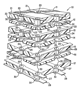
Fig. l is a partially diagrammatic top view in plan of a
matrix assembly constructed in accordance with the principles
of the present invention.
Fig. 2 is an enlarged top view in plan of the upper right
corner portion of the matrix assembly of Fig. l.
Fig. 3 is an exploded perspective view in section of a
portion of the matrix of Fig. l.
Fig. 4 is a view in elevation of a circuit jumper pin
utilized to make connections between traces in the matrix
assembly of Fig. l.
Fig. 5 is a top view in plan of a pick and place mechanism
for inserting circuit jumper pins in, and removing circuit
jumper pins from, the matrix assembly of Fig. l.
Fig. 6 is a view in elevation and partial section of the
pick and place mechanism of Fig. 5.
Fig. 7 is a sectional view in elevation of a portion of
the matrix assembly of Fig. l illustrating the manner in which
the circuit jumper pin, permanent jumper rods, and external
connector pins engage various traces on the matrix circuit
boards.
Fig. 8 is an electrical schematic diagram of a portion of
the matrix of Fig. l illustrating the manner in which external
connectors engage traces on the various circuit boards.
Fig. 9 is a partially diagrammatic view in perspective of
a portion of the four circuit board layers in the matrix of
Fig. l, illustrating the manner in which external connections
are made to the circuit boards.
W095/06344 ~ 1 6 ~ ~ 6 3 PCT~S94/09140
Fig. 10 is an electrical block diagram of the system for
controlling the pick and place mechanism of Fig. 6.
.
BRIEF DESCRIPTION OF THE PREFERRED EMBODIMENTS
Referring to Figs. 1 - 3 of the accompanying drawings, a
matrix assembly 10 comprises four stacked planar circuit boards
11, 13, 15 and 17 of generally rectangular configuration. As
viewed in Fig. 3, circuit board 11 is the first or top board
and is designated herein as the switch tip board. Circuit
board 13 is the second board and is designated herein as the
subscriber tip board. Circuit board 15 is the next board in
sequence and is designated herein as the subscriber ring board.
Circuit board 17 is the bottom board and is designated herein
as the switch ring board. Designations such as "top" and
"bottom" are used for convenience only and are not to be
construed as limiting the orientation of matrix assembly 10.
An electrically insulative planar board 12 is disposed in
abutting relationship between circuit boards 11 and 13 and is
substantially coextensive in width and length with those
circuit boards. A similar insulative board 14 is disposed
between circuit boards 13 and 15, and another insulative board
16 is disposed between circuit boards lS and 17. These circuit
and insulative boards are compressed together by a plurality
of rivets, or the like, to provide a compact assembly with each
insulative board in abutting contact on each of its surfaces
with an adjacent circuit board.
Multiple matrix holes 20 are drilled or otherwise formed
through the entire assembly, including all of the seven boards
11 through 17, in a direction perpendicular to the board
surfaces. Matrix holes 20 are formed in patterns or groups
but, in general form an overall grid-like array. In the
particular embodiment illustrated in Fig. 1, there are twenty-
five of these patterns designated with respective letters A
through Y. Within each of patterns A through Y the matrix
holes 20 are arranged in columns and rows. The number of
matrix holes in each pattern may be different or the same.
Furthermore, while it is conceivable that the patterns can be
W095/06344 PCT~S94/09140
3 8
other than a grid of columns and rows (e.g., a radial pattern,
etc.), the grid pattern is particularly advantageous. In this
regard, the columns and rows of matrix holes 20 in each pattern
are aligned with corresponding columns and rows of adjacent
patterns to define one large matrix hole grid made up of all
the smaller pattern grids.
On the top (i.e., exposed) surface of switch tip circuit
board 11 there are multiple conductive switch tip traces 21
arranged linearly in spaced parallel relation. Switch tip
traces 21 are typically plated onto the board surface by known
techniques. Each switch tip trace or conductor 21 extends
along a respective row of matrix holes 20, whereby each row of
matrix holes 20 in circuit board 11 has a respective trace 21.
Corresponding switch tip traces 22 are plated onto the
underside (i.e., interior) surface of circuit board 11 in
precise registry with respective traces 21 on the opposite
surface of board 11. Matrix holes 20 extending through the
board are conductively plated in a conventional manner to form
female contacts 30 (see Fig. 3) interconnecting their
respective traces 21 and 22 at each hole 20. In addition to
interconnecting traces 21 and 22, female contacts 30 serve to
permit interconnections between different circuit boards as
described hereinbelow.
The subscriber tip circuit board 13 has multiple
subscriber tip traces 23 arranged linearly in parallel spaced
relation on its top surface. Identical multiple subscriber tip
traces 24 are defined on the bottom surface of board 13 in
precise registry with respective traces 23. Plated female
contacts 30 are also provided in the matrix holes 20 of board
13. Traces 23 and 24 extend along respective columns of holes
20 and are electrically connected by female contacts 30.
Subscriber tip traces 23 and 24 extend orthogonally relative
to switch traces 21 and 22 on circuit board 11.
On the subscriber ring circuit board 15 there are
subscriber ring traces 25 and 26 disposed at the top and bottom
surfaces of the board, respectively, in an array identical to
that for traces 23 and 24 of circuit board 13, that is,
~ W095/06344 2 ~ 6 9 ~ ~ 3 PCT~S94/09140
9 .
orthogonally to traces 21 and 22 on circuit board 11. On the
switch ring circuit board, opposite surface traces 27 and 28
are arranged parallel to traces 21 and 22. It will be
appreciated, therefore, that the switch traces on circuit
boards 11 and 17 are parallel to each other but orthogonal to
the traces on circuit boards 13 and 15.
The traces and female contacts 30 on each board are
insulated from the traces and female contacts on successive
circuit boards by the adjacent insulation boards 12, 14 and 16
interposed between and abutting successive circuit boards. It
will be appreciated, however, that any switch tip trace on
circuit board 11, for example, can be electrically connected
to any subscriber tip trace on circuit board 13 by providing
a connection between female contacts 30 of the two circuit
boards at the matrix location where the two orthogonally
related traces cross. A novel circuit jumper pin 40 for
effecting such a connection is illustrated in Fig. 4 to which
specific reference is now made.
Circuit jumper pin 40 is an elongated member having a grip
41 at its proximal end and a tapered tip 43 at its distal end.
Grip 41 is generally cylindrical with a predetermined diameter
and a tapered proximal end. Pin 40 is made of an electrically
insulative plastic material that is somewhat flexible in order
to preclude breakage when the pin sub~ected to bending forces
or off-axis longitudinal compression but sufficiently rigid to
permit the pin to be inserted through a set of aligned matrix
holes 20 in matrix assembly 10. In this respect the diameter
of pin 40 is smaller than the inner diameter of female contacts
30. An annular stop flange 45 extends radially from pin 40 at
a location closer to the proximal end than the distal end of
the pin. Proximally of stop 45 the pin has a short cylindrical
section 44 with a diameter similar to the diameter of grip 41.
Between section 44 and grip 41 there is a reduced diameter
cylindrical section 46. Stop flange 45 has a diameter greater
than that of holes 20 and divides the pin into insertable and
non-insertable length portions. Specifically, the insertable
pin portion is located distally of stop flange 45, the depth
W095/06344 PCT~S94/09140
3 lo
of insertion into a matrix holes 20 being limited by abutment
of flange 45 against the exposed top surface of circuit board
11. The length of the insertable portion of pin 40 is such to
permit distal tip 43 to extend through and beyond the bottom
circuit board 17 when the pin is fully inserted into the matrix
assembly (see Fig. 7).
The portion of pin 40 extending between the female
contacts 30 of circuit boards 11 and 13 is surrounded by a tip
contact sleeve 47 of electrically conductive spring-like
material. A similarly configured ring contact sleeve 49
simultaneously extends between the female contacts 30 of
circuit boards 15 and 17. Contact sleeves may take the form,
for example, of MC-Multilam LAV band-type contacts sold by
Multi-Contact USA of Santa Rosa, California. When unstressed
(i.e., radially uncompressed), sleeves 47 and 49 have diameters
slightly larger than the inner diameter of female contacts 30.
When pin 40 is fully inserted in a set of matrix holes 20, tip
sleeve 47 extends between and is radially compressed by aligned
female contacts 30 on switch tip board 11 and subscriber tip
board 13. This radial compression of the resilient conductive
sleeve assures positive electrical contact between the sleeve
and the female contacts, thereby assuring connection between
the corresponding switch tip trace conductors 21, 22 and the
subscriber tip trace conductors 23, 24. Similar connection is
made between the subscriber ring trace conductors 25, 26 and
the switch ring trace conductors 27, 28 by ring sleeve 49.
It will be appreciated that any switch tip trace 21, 22
can be electrically connected to any subscriber tip trace 23,
24 by simply inserting a pin 40 into the matrix holes 20
corresponding to the crossover location of the traces to be so
connected. The ring trace for the same subscriber and the ring
trace for the same switch line cross at the same matrix holes
20 so that a complete tip and ring connection between the
subscriber and the switch can be made with a single circuit
jumper pin 40. Pin 40 can be manually inserted and removed by
grasping proximal grip 41 in one's hand and moving the pin
axially in the desired direction. The tapered distal end 43
W095/06344 PCT~S94/09140
11
on the pin facilitates insertion. By rendering the pin
somewhat flexible, a slight axial misalignment of the pin
during insertion will not hinder insertion and, more
importantly, will not cause the pin to break due to axial
bending forces.
Of course, the greatest advantage of the structure
described above relates to the capability of inserting pins 40
into matrix holes 20 by remote control. A pin picker and
placer mechanism capable of being remotely controlled for this
purpose is illustrated in Figs. 5 and 6 to which specific
reference is now made. As shown schematically in Fig. 5, a
carriage 50 is supported in spaced relation to matrix assembly
10 on a pair of parallel guide rods 51, 53 extending parallel
to the Y-axis of the matrix. A threaded receiver 55 on
carriage 50 engages a ball screw 57 extending parallel to guide
rods 51 and 53. Ball screw 57 is selectively rotatable by a
step motor 59 to permit positioning of carriage 50 stepwise
along the Y-axis. Motor 59 is mounted on a guide block 60
supporting one end of each guide rod 51 and 53. The other ends
of these rods are supported in another guide block 61 disposed
at the opposite side of matrix assembly 10. A pair of guide
rails 63, 65 extend along the X-axi~ of matrix 10 on opposite
sides of the matrix. Rail 63 is secured at its end to supports
62 and 64; rail 65 is secured at its end to supports 66 and 67.
Guide block 60 engages a ball screw 68 and is slidable on guide
rail 63. Guide block 61 is slidable on guide rail 65. A step
motor 70 selectively rotates ball screw 68 to move guide block
60 along rail 63 to successive locations on the X-axis of the
matrix. As a conse~uence, guide rods 51, 53 are translated
perpendicular to their longitudinal axis along with guide block
61, the latter sliding along guide rail 65. It will be
appreciated, therefore, that carriage 50 is selectively movable
along the matrix X-axis by step motor 70 and along the matrix
Y-axis by step motor 59. The spacing between matrix holes 20
corresponds to an integral number of motor steps so that
carriage 50 can be controllably positioned at any matrix hole
once it has been placed at a known reference position.
W095/u6344 Z ~ ~ g 5 6 3 PCT~594/~914~
As best illustrated in Fig. 6, carriage 50 includes a
support plate 71 with spaced sleeves 73, 75 for slidably
receiving guide rods 51, 53, respectively. A lead screw 76
extends perpendicularly through support plate 71 to engage a
picker platform 80 disposed in parallel spaced relation to the
support plate. A lead screw drive motor 77 secured to support
plate 71 selectively rotates a nut secured internally of the
motor to cause the motor to move along the fastened lead screw
to move platform 80 closer to and farther from the support
plate. A pair of spaced guide rods 78, 79 are slidable through
respective guide sleeves 81, 82 on plate 71 and have their
distal ends fixedly secured to platform 80 to facilitate guided
movement of the platform relative to the support plate.
Disposed centrally of platform 80 there is defined a
frusto- conical through hole 83 having a diameter that
decreases in a distal direction. A picker nut 84 has a frusto-
conical proximal end, matching the periphery of frusto-conical
hole 83, disposed in the hole and threadedly engaging a hollow
threaded stud 85 secured to and projecting from the distal end
of a solenoid 86. Solenoid 86 is disposed at the proximal
surface of platform 80 with its hollow stud 85 projecting
perpendicular to platform 80 and into hole 83. An annular
retaining washer 87 is secured to the proximal surface of
platform 88 to prevent nut 84 from moving axially beyond the
proximal surface of platform 80. Retaining washer 87 surrounds
the solenoid in coaxial relation with hole 83 and has an inner
diameter smaller than the diameter of hole 83 at the platform
proximal surface. An annular spring washer 88 is disposed in
hole 83 between the proximal surface of nut 84 and the distal
surface of ret~ining washer 87 to permit some degree of
resiliency in the assembly as described below.
The armature 90 of solenoid 86 is a rod disposed coaxially
in hole 83 and extending through threaded stud 85 into the
hollow interior of nut 84. The distal end of nut 84 is
configured as a hollow picker tube 91 with a sufficiently large
inner diameter to permit free longitudinal movement of armature
rod 90 therein. The inner diameter of picker tube 91 is also
~ W095/06344 ~ ~ ~ 9 5 ~ 3 PCT~594/n9l4~
equal to or just slightly larger than the diameter of grip 41
of circuit ~umper pin 40 in order to permit the grip to be
longitudinally received in the tube and frictionally engaged
therein. A small radial protuberance 92 from the inner wall
of picker tube 91 is positioned longitudinally to be received
in the recessed section 46 of circuit jumper pin 40 to
positively retain the pin in the picker tube and prevent
inadvertent disengagement.
A bracket 93 is secured to solenoid 86 and supports an
electrical switch 94 having an actuator button 95 axially
aligned with the solenoid armature rod 90. Actuator button 95
is positioned to be depressed, thereby actuating the switch,
when rod 90 is in its fully retracted position.
In operation, when it is desired to pick a circuit ~umper
pin 40 from a particular matrix hole 20, carriage 50 is stepped
to the X-Y location of that hole by step motors 59 and 70.
Accordingly, once carriage 50 has reached the desired X-Y
location, lead screw drive motor 77 is energized to rotate lead
screw 76 and move platform 80 toward the matrix assembly. At
this time solenoid 86 is not actuated so that armature rod 90
is freely movable within picker tube 91. Since there is no
proximally directed force applied to rod 90, the rod cannot
depress actuator button 95 to actuate switch 94. As the open
distal end of picking tube 91 reaches pin 40, grip portion 41
of the pin enters the tube, gradually pushing rod 90 in a
proximal direction. Maximum insertion of pin 40 into tube 91
corresponds to protuberance 92 extending radially into the
recessed diameter section 46 of the pin. In this position of
the pin, rod 90 is forced by the pin against actuator button
95 to actuate switch 94, thereby signifying that the pin is
engaged. Lead screw motor 77 is then operated in the reverse
direction to move platform 80 and the engaged pin 40 away from
matrix 10. This movement continues until the engaged pin is
retracted to a location where it will not interfere with other
inserted pins once carriage 50 begins to move. Thereafter, the
carriage is moved by motors 59 and 70 to a matrix hole location
where the engaged pin is to be placed. Once carriage 50 and
W095/06344 2 ~ 6 ~ ~ ~ 3 14 PCT~S94/09140
the engaged pin 40 reach the selected location, motor 77
rotates to move along lead screw 76 to again move platform 80
toward the matrix assembly. This movement continues until the
engaged pin is inserted into the matrix hole at the carriage
location. Stop~flange 45 on the engaged pin limits axial
movement of the pin through the aligned holes 20. Once this
limit is reached, solenoid 86 is energized and applies a
distally directed force to armature rod 90 which, in turn,
transmits this force axially to the engaged pin. Rod 90 cannot
move, however, because stop flange 45 prevents distal movement
of the engaged pin. Lead screw motor 77 may then be actuated
in the reverse direction to move platform 80 and picker tube
9l away from matrix l0. As the picker tube begins to move, the
distally directed force applied to pin 40 through rod 90 by the
energized solenoid becomes capable of disengaging the pin from
protuberance 92 and forcing the pin out of picker tube 90. The
disengaged pin thus remains in the matrix holes in which it has
been placed. Distal movement of pin 40 relative to tube 9l
permits rod 90 to move distally, thereby removing the actuating
force from actuator button 95 of switch 94. It will be
appreciated, therefore, that switch 94 is only actuated when
a pin 40 is positively engaged in picking tube 9l. The
information that a pin is presently engaged is useful in the
automatic process of pin picking and placement in order to
permit appropriate sequential operation of the motors and
solenoids.
During a pin picking operation, if the picking tube 9l is
slightly off axial center relative to the pin 40 to be picked,
the proximal end of the pin impinges against the distal annular
edge of the tube. The tapered proximal end of impinging pin
grip 45 assists in assuring that the pin is properly guided
into tube 9l as the tube continues to move toward matrix l0.
In addition, resilient slack in tube 9l is created by spring
washer 88. In particular, if the proximal end of grip 45 is
urged against the annular edge of tube 9l, a torque is applied
to the tube and to nut 84 against the resilient bias of spring
washer 88. This torque tends to rotate tube 9l off axis in a
~9~
WO95/06344 ^ PCT~S94/09140
direction that urges the tube axis closer to the axis of pin
40. The result is to further facilitate entry of the pin into
the distally moving picker tube 91. Once the torque is removed
(i.e., the pin has been engaged), spring washer 88 acts to re-
center nut 84 and its picker tube 91. When an engaged pin is
~ in the process of being moved axially toward a matrix hole 20
for placement therein, it is possible that the distal end of
the pin may be slightly off center relative to the receiving
hole 20. The tapered distal tip 43 of pin 40 acts to
facilitate entry of the pin into the intended matrix hole. In
addition, the resilient slack afforded by spring washer 88
permits off-axis tilting of the picker tube and the engaged pin
to further facilitate pin placement. Again, automatic re-
centering of nut 84 and tube 91 is effected by the spring
washer after the pin has been released. It will be appreciated
that other arrangements for effecting automatic re-centering
can be employed within the scope of this invention. In this
regard, the solenoid mounting arrangement need not include a
frusto-conical nut and spring washer arrangement; rather any
mounting structure capable of automatically re-centering the
solenoid mounting may be used.
External connections to matrix assembly 10 are made at the
exposed surface of the switch ring board 17 in a manner
illustrated in Figs. 7, 8 and 9. In particular, a plurality
of multiple pin circuit board connectors 101 (only one
connector being illustrated in Figs. 7 and 9 for purposes of
preserving clarity) are plugged into plated connector holes 112
provided at the exposed surface of switch ring circuit board
17 about the periphery of the matrix holes. This is the
opposite surface of the matrix assembly from the surface at
which the jumper pins 40 are inserted into the matrix holes 20.
Circuit board connectors 101 may be the type sold as Action Pin
connectors by AMP, Inc. of Harrisburg, Pennsylvania. Each
connector 101 has two parallel rows of connector pins 102, an
inboard row closer to the adjacent matrix pattern and an
outboard row closer to the periphery of board 17. The inboard
connector pins 102 serve to connect traces on circuit board 17
w095/06344 ~ 5 ~ 3 pcT~ss4losl4n
16
to an external cable 105 via a cable termination connector 106
plugged into the circuit board connector 101. In order to
provide external connection to and from the other circuit
boards 11, 13 and 15, a variety of different techniques may be
employed. In the illustrated embodiment, the preferred
technique for bringing traces 21, 22 from circuit board 11 to
a board connector 101 is to first extend the corresponding
trace 21, 22 to a corresponding housekeeping plating hole 20a
located near the periphery of board 11. For example, referring
to Fig. 1 and particularly to matrix pattern J, traces 21, 22
extend to a single column of housekeeping holes 20a disposed
along the right side of the pattern. These holes, in turn, are
connected by conductive traces to respective jumper holes 110
in a parallel column of jumper holes extending along the
adjacent board periphery. An electrically conductive jumper
rod 103 (Fig. 7) is employed to jump traces from the switch tip
board 11 to the switch ring board 17 and ultimately into
contact with respective pins 102 of one of the connectors 101.
For this purpose there are multiple sets of jumper holes 110
defined through each of boards 11 through 17 adjacent the board
peripheries. These jumper holes are typically of smaller
diameter than matrix holes 20 and are best illustrated in Figs.
1, 2, 7 and 9. The jumper holes 110 in the various boards are
aligned to provide respective jumper channels extending
depthwise through the entire depth or thickness of matrix
assembly 10. There is one such jumper channel for each matrix
subscriber tip and switch tip conductor trace. In order to
jump a conductor trace from board 11 to board 17, for example,
the corresponding jumper hole 110 on board 11 is conductively
plated at 111 (Fig. 7) so as to interconnect the two juxtaposed
traces on opposite surfaces of board 11.
The aligned jumper hole 110 on board 17 is similarly
conductively plated at 111 to join respective traces on
opposite surfaces of that board. A jumper rod 103 is inserted
through the channel comprised of the aligned jumper holes 110,
and is soldered at its ends to the plating 111 in the holes on
boards 11 and 17. Jumper rod 103 thus brings the selected
2169~3
WO95/06344 17 PCT~S94/09140
trace from board 11 to board 17 where rod 103 contacts a
respective trace 33 via the plating 111 in the jumper hole in
board 17. Trace 33 extends to one hole 112 of an outer row of
plated connector holes 112 on board 17 where the trace contacts
an outboard pin 102 of connector 101 for external connections
of the signal.
It is noted that there are two rows of connector pin
receiving holes 112 for each connector 101, namely an outer row
disposed closer to and adjacent a row of jumper holes 110, and
an inner row disposed closer to the matrix holes 20. These
rows correspond to and receive respective outboard and inboard
rows of pins 102 of connector 101. The holes 112 in the outer
row are all connected by traces 33 on both surfaces of board
17 to respective jumper holes 110. Holes 112 in the inner row
are connected to respective housekeeping holes 20a disposed on
board 17 in three rows located between the connector pin holes
112 and the matrix holes 20.
In order to provide external connections for traces 23,
24 on circuit board 13, the trace must be connected to an
available housekeeping hole 20a on circuit board 11. To
accomplish this, a circuit jumper pin 40 is employed. In
particular, and referring to Fig. 7, a subscriber tip trace
23, 24 (shown going into the plane of the Fig. 7 drawing) is
brought to one of the housekeeping holes 20a of a row of such
holes 20a extending along an edge of the matrix on board 13.
The housekeeping holes 20a are identical to matrix holes 20 in
size and shape and are plated with female contacts 30a similar
to female contacts 30. When a circuit jumper pin 40 is
disposed in a housekeeping hole 20a, the proximal conductive
sleeve 47 of the circuit jumper pin 40 connects the female
contact 30a of board 13 to an aligned female contact 30a of
board 11, thereby permitting the external subscriber tip signal
to be jumped between these boards. From board 11 the external
subscriber tip signal is brought to a jumper hole 110 on board
17 and to an outer connector pin hole 112 in the same manner
described above for bringing an external switch tip signal from
Wo 95/06344 ~ 18 PCT/US94/09140
board 11 to board 17 (i.e., by means of a dedicated jumper rod
103).
Subscriber ring signals on board 15 can be brought to
board 17 for external connection in either of two ways. In one
approach the connector pins 102 from connector 101 make direct
contact with a plated connector pin hole 112 in board 15. The
preferred approach, however, is to permit the distal conductive
sleeve 49 of a circuit jumper pin 40 to jump the signal between
boards 15 and 17 at aligned housekeeping holes 20a. In either
case, the aligned connector pin through holes 112, some of
which are plated as required to contact connector pins 102,
permit external connection via connector 101. Pins 112 are
arranged in two rows positioned, as best illustrated in Fig.
8, to receive the two rows of pins 102 of connectors 101. Each
hole 112 in the outer row is connected by a circuit board trace
33 to a respective jumper pin 110 on board 17 to permit the tip
signals from boards 11 and 13 to be connected to the
corresponding row of connector pins 102. The holes 112 in the
inner row are connected to corresponding housekeeping holes 20a
on board 17 to permit connection of ring signals from boards
15 and 17 to the corresponding inboard row of connector pins
102. The switch ring traces on board 17 can be brought
directly to respective housekeeping holes along board 17 to
provide access to an inner connector hole 112 on that board.
As noted above, it is possible to manually place a circuit
~umper pin 40 into a particular set of aligned matrix holes 20
to connect the tip and ring signal lines of the corresponding
subscriber to respective selected signal switch tip and switch
ring signal lines for connection to the local switch and then
via a digital carrier line to a central office. The most
advantageous use of the present invention, however, is to place
pins 40 in matrix holes 20 with the picker and placer mechanism
(Figs. 5 and 6) controlled remotely from the central office.
A generalized block diagram of equipment located at the remote
station and permitting such remote control is provided in Fig.
10 to which specific reference is now made.
WO 95/06344 ~ ~ ~ 9~ ~i 3 PCT/US94/09140
.
19
Control signals from a telephone system central office are
received by a modem 129 having an interface 130 arranged to
format the signals and distribute them via a microprocessor bus
131 to a microprocessor 132. Bus 131 provides signal
communication between the microprocessor and all of the
controlled e~uipment and data processing circuits at the remote
station. Microprocessor 132 controls operation of the
equipment at the remote station, including X-axis step motor
70, Y-axis step motor 60 and Z-axis step motor 77. A non-
volatile read/write random access memory (RAM) 133 is provided
to store the status (i.e., whether or not occupied) of the
various matrix locations, the housekeeping hole locations and
the circuit jumper pins 40. A read only memory (ROM) 134
stores the operating system program and application program to
operate the microprocessor. A volatile RAM 135 serves the
function of transient working storage.
The X-axis step motor 70 is controlled by an X-stepper
motor translator 136 which in turn is controlled by a X-stepper
indexer 137. Translator 136 and indexer 137 are commercially
available components used in a conventional manner to control
stepping motors. Translator 136, for example, may be a model
NEAT SDM7, manufactured by New England Affiliated Technologies,
while indexer 137 may be a model INDEXER LPT (using line
printer controller) manufactured by Ability Systems
Corporation. In response to control signals received from
microprocessor 132 via bus 131, X-stepper indexer 137 applies
step and direction signals to the x-stepper translator 136.
The translator responds by applying appropriate phase control
signals to motor 70 to positionally step guide block 60 (Fig.
5) horizontally (i.e., in the X-direction).
Y-axis step motor 60 is controlled by a Y-stepper
translator 138 and Y-stepper indexer 139 which are
substantially the same as translator 136 and indexer 137,
respectively, to positionally step guide block 50 (Fig. 5)
vertically (i.e., in the Y-direction). Likewise, step motor
77 is controlled by a similar Z-stepper motor translator 141
wosslo6344 PCT~S94109140
2~ 20
and Z-stepper indexer 142 to positionally step platform 80
(Fig. 6) in the Z-direction.
For purposes of simplicity and to facilitate understanding
of the invention, the embodiment illustrated and described
above shows only one pick and place mechanism. In practice,
it is more efficient to subdivide the matrix into two or more
sections, whereby two or more carriages 50 are employed to
exclusively serve respective matrix sections. This would
permit quicker access to pins 40 and matrix holes 20 since the
carriages would have shorter distances to travel. As an
example of such a subdivision, reference is made to Fig. l
wherein a substantially diagonal line 150 subdivides the matrix
into two electrically isolated sections. For such an
arrangement, signal traces on the various boards would not
extend past line 150 so that each half of the matrix
exclusively serves its own set of subscriber and switch lines.
It is possible, with the disclosed embodiment, to connect
a subscriber pair (i.e., tip and ring traces) from one matrix
assembly lO to a switch pair on another matrix assembly. For
example, the situation may arise where there is no unused
switch pair available on one matrix assembly for a subscriber
pair on that assembly requiring connection to a switch pair.
Under such circumstances the subscriber pair can be connected
externally of its matrix assembly, in the manner described
above (i.e., via a connector lOl, etc.), to the assembly
containing the unused switch pair. In this regard, one or more
matrix sections of the matrix assembly may be reserved for
providing the necessary connection points to permit connections
between the assemblies.
Although in the disclosed preferred embodiment of the
invention the connections made by the circuit jumper pins 40
are between orthogonally related traces on two successive
circuit boards, the traces to be connected can be other than
orthogonally related (i.e., at any angle, parallel, radial
traces on one board connected to circular traces on another
board, etc.). The important feature is that the matrix holes
20 be provided through the traces and the sandwiched boards at
~ wo gs/n6344 ~ :~ 6 9 5 ~ 3 PCT/U594l09l4n
the proposed interconnection points to permit the radially
flexible electrically conductive sleeve of a non-conductive
longitudinally flexible pin to interconnect the traces on the
two boards.
It will be appreciated that, although the preferred
embodiment disclosed herein provides for esch circuit jumper
pin 40 to make two separate connections, the pins and boards
can be arranged to provide for any number of connections made
by an inserted pin. For example, if only two circuit boards
are used, only one connection is made; if six circuit bosrds
are used, three connections are made; if 2x circuit boards are
used, x connections are made. Each connection between a pair
of circuit boards requires a respective conductive sleeve to
be appropriately positioned along the circuit jumper pin. It
will also be appreciated that more than two conductors can be
connected together using the principles of the present
invention. For example, if it is desired to selectively
interconnect three (or more) conductors on three circuit boards
via aligned matrix holes, it is only necessary to extend the
length of the conductive sleeve on the circuit jumper pins to
permit the sleeve to extend between three or more circuit
boards.
It is preferred that the female contacts 30 in the matrix
holes 20 be plated with gold over nickel to provide a durable,
low electrical resistance connection having high resistance to
corrosion. Of course, any conductive hole-plating technique
may be employed. Contact sleeves 47, 49 are preferably made
of hardened spring material, such as beryllium-copper, and are
also preferably coated with gold over nickel. The non-
conductive body of pin 40 is made of any suitable molded
plastic material, with Delrin being the preferred material.
Matrix holes 20 and pins 40 have been disclosed as having
peripheries encompassing circular areas; however, other
peripheral configurations may be employed within the purview
of the invention. By way of example, elliptical or polygonal
peripheries are possible, certainly for systems wherein the
pins are manually inserted into the matrix holes. For remotely
W095/06344 PCT~S94/09140
3 22
controlled pin positioning, certain peripheral configurations
may require apparatus for assuring proper angular orientation
of the pin before it is inserted into a hole. It is also
within the scope of the invention to provide female contacts
30 in a configuration other than completely surrounding the
matrix holes; that is, a female contact may be plated only over
a portion of the periphery or only over a portion of the axial
length of the matrix hole.
One aspect of the invention involves utilizationM of
plural carefully registered circuit boards having plated
through holes serving as the passive member in each selected
cross-connection made by the active member (i.e., the circuit
~umper pin). Typically, the matrix assembly is formed by
drilling the matrix holes in all of the boards simultaneously
to assure hole registration. After drilling, the holes are
plated on each individual circuit board, and then all of the
boards are laminated together with insulative boards interposed
between the circuit boards. In the disclosed embodiment, the
resulting structure forms two matrices, one for the tip signals
and the other for the ring signals.
In the preferred embodiment, matrix holes 20 have
diameters of 0.078 inches and have their centers spaced by
0.140 inches. The spacing being circuit boards 11 and 13, snd
between circuit boards 15 and 17 is 0.031 inches. The axial
length of contact sleeves 47, 49 when unstressed is .190
inches; the outside diameter of those sleeves when unstressed
is .085 inches. The length of the portion of the body of pin
40 from flange 45 to the remote end of distal tip 43 is .460
inches. Flange 45 has a diameter of .130 inches and an axial
length of .050 inches.
From the foregoing it will be appreciated that the
invention makes available a novel method and apparatus for
efficiently and inexpensively making connections between two
or more circuits, either manually or, most advantageously,
automatically. The primary intended utilization of the
invention is to provide an automated means for connecting
telephone lines in a telephone central office to cable pairs
095/06344 2 ~ S ~ 3 PCT~S94/09140
23
going to subscriber locations. The invention can be utilized
in any application requiring an easily configurable matrix
cross-connect arrangement that is both inexpensive and
reliable.
Having described preferred embodiments of a new and
improved cross-connect system in accordance with the present
invention, it is believed that other modifications, variations
and changes will be suggested to those skilled in the art in
view of the teachings set forth herein. It is therefore to be
understood that all such variations, modifications and changes
are believed to fall within the scope of the present invention
as defined by the appended claims.
~ r~ s~F~ ¢~ ~