Note: Descriptions are shown in the official language in which they were submitted.
2 ! 69706
.
- 1 -
CIRCUIT AND METHOD FOR BATTERY CHARGE CONTROL
Background of the Invention
The present invention relates in general to battery cell
monitoring and charging and, more particularly, to battery cell
charge balancing.
Batteries are used in a wide variety of applications
including digital pagers, cellular telephones, notebook computers,
and in general, portable consumer electronics. Batteries
employed in portable electronics include lithium ion, lithium
polymer, nickel-cadmium, or nickel-metal hydride compositions.
Since many of the applications require potentials of 12.0 volts or
greater, multiple battery cells are often serially connected in a
battery pack to provide the required operating potential. Once the
batteries have been discharged by shelf life or during normal use
in an application, it becomes necessary to recharge the battery
pack. Problems of overcharging and undercharging of cells are
encountered when battery packs are exposed to the recharging
process. Overcharging of cells results in potentially dangerous
and catastrophic failures in lithium based chemistries while
over-discharged cells experience decreased cell life for all
battery chemistries.
In the prior art, battery monitoring and charging schemes
have been developed that continuously monitor all battery cells
simultaneously within a battery pack to monitor their status and
likewise, charge all cells within the battery pack in a serial
fashion. A voltage differential may develop over a history of
many charging cycles if cells in the battery pack are not evenly
matched. Thus, when the charging process is enabled, a more
severe overcharge is created for one cell with respect to the
other cells causing a safety concern in the overcharged cell.
Hence a need exists to monitor and charge the individual
cells of a battery pack in a balanced fashion, without undue drain
on the battery pack.
21 69706
- 1 (a) -
Summary Of The Invention
An object of the present invention is to provide a circuit and a
method for battery charge control to monitor and charge the individual
cells of a battery pack in a balanced fashion, without undue drain on the
batty pac in a balanced fashion, without undue drain on the battery
pack.
In accordance with an aspect of the present invention, there is
provided a battery charge control circuit coupled to a first battery cell.
The circuit comprises a measurement circuit, a control circuit and a
discharge circuit. The measurement circuit is coupled for receiving a
first battery voltage from the first battery cell and providing a status
signal upon sensing an overvoltage condition in the first battery cell.
The control circuit is responsive to the status signal for decoding a first
battery control signal from the status signal. The discharge circuit is
coupled across the first battery cell and operating in response to the first
battery control signal for discharging the first battery cell.
- 2 ~ 69706
Brief Description of the Drawings
FIG. 1 is a schematic and block diagram illustrating a
5 battery charging circuit for a battery pack;
FIG. 2 is a schematic diagram illustrating the over-voltage
logic of FIG. 1;
FIG. 3 is a schematic diagram illustrating the under-voltage
logic of FIG. 1;
10FIG. 4 is a schematic and block diagram illustrating a
discharge select logic of the control circuit of FIG. 1;
FIG. 5 is a schematic diagram illustrating a multiplexer
select logic of the control circuit of FIG. 1;
FIG. 6 is a set of logic tables illustrating the logic function
15of the discharge select blocks of FIG. 5;
FIG. 7 is a schematic diagram illustrating the hysteresis
circuit of the control circuit of FIG. 1;
FIG. 8 is a table illustrating the logical operation of the
battery charging circuit of FIG. 1.
20FIG. 9 is a schematic diagram illustrating the pack sense
circuit of FIG. 1;
FIG. 10 is a schematic diagram illustrating the over-current
detector circuit of FIG. 1;
FIG. 11 is a schematic diagram of the over-current logic
25circuit of FIG. 1;
FIG. 12 is a table illustrating the operation of the over-
current logic circuit of FIG. 11;
FIG. 13 is a table illustrating the operation of the over-
current logic circuit of FIG. 11; and
30FIG. 14 is a table illustrating the functions of the battery
charging circuit of FIG. 1.
- 21 69706
-- 3 --
Detailed Description of the Preferred Embodiment
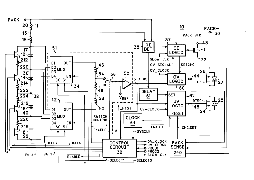
Referring to FIG. 1, battery charge control circuit 10 is
5 shown suitable for manufacturing as a monolithic integrated
circuit (IC) using conventional integrated circuit processes.
Battery cells 12, 14, 16 and 18 are serially coupled between
power supply conductor 20 (PACK+) and node 22 power supply
conductor. Battery cells 12, 14, 16 and 18 are preferably lithium
10 ion or polymer type rechargeable batteries, where the lithium ion
cells operate at 4.2 volts and the polymer cells operate at 3.0
volts under a full charge. PROG1 and PROG2 inputs to control
circuit 32 provide for a binary programming code representing the
total number of battery cells presented to battery charge control
15 circuit 10. A list of binary programming codes for up to four
battery cells is shown in Table 1. If fewer than four battery cells
are present in the battery pack, the cells are replaced with a
short circuit. For example, if three cells are programmed, battery
cell 12 is replaced with a short circuit. Additional PROG inputs
20 are incorporated to accommodate a battery system having more
than four cells.
T~hle 1
Number of cells PROG1 Input PROG2 Input
4 0 0
2 1 0
0
Current sense resistor 11 and current sense resistor 15 are
25 serially coupled between power supply conductor 20 and battery
cell 12. Node 22 is coupled to the source of discharge transistor
24. The drain of transistor 24 is coupled to the drain of charge
transistor 26. The source of transistor 26 is coupled to power
supply conductor 30 (PACK-). Diode 25 has an anode coupled to
30 the source of transistor 24 and a cathode coupled to the drain of
2l ~9706
_
-- 4 --
transistor 24. Diode 25 is inherent in the structure of transistor
24. Diode 27 has an anode coupled to the source of transistor 26,
and a cathode coupled to the drain of transistor 26. Diode 27 is
inherent in the structure of transistor 24. Power supply
5 conductors 20 and 30 represent the positive and negative
terminals of the battery pack formed by battery cells 12-18.
Transistor 24 receives a DISCHARGE (DISCH) signal at node 45
from the output of under-voltage logic (UV logic) circuit 62. The
gate of transistor 26 is coupled to the output of OV logic circuit
10 60, at node 44, to receive a CHARGE (CHG) signal. An input of OV
logic circuit 60 is coupled to receive the SET CHARGE (SET CHG)
signal from an output of over-current logic (Ol logic) circuit 37.
Transistor 41 has a drain coupled to node 22, a gate coupled to an
output of over-current logic circuit 37, and a source coupled to a
15 terminal 43 for connection to an external resistor located within
a battery charger. Transistor 41 could also be a bipolar
transistor. Ol logic circuit 37 receives a signal from the output
of over-current detect circuit (Ol detect) 35, the SLOW CLOCK
signal from control circuit 32, and the OV signal from OV logic
20 circuit 60.
Transistor 41 of Ol logic circuit 60 simulates the behavior
of a thermistor. Nickel technology based battery chargers have a
terminal that is used for a thermistor connection. As an
advantage of the present invention, when a lithium technology
25 battery pack is coupled to a nickel technology battery charger,
transistor 41 is activated, causing the battery charger to operate
in a trickle current charge mode. The thermistor simulation
device disables the large value nickel technology charging
currents that normally are applied to the battery pack. The
30 lithium technology battery pack is therefore protected from
dangerous overcharging.
The inputs of Ol DETECT circuit 35 are coupled across sense
resistor 11. Ol DETECT circuit 35 has a second output coupled to
the SET input of UV logic 62 through delay circuit 61. When an
35 over-discharge current is detected by Ol DETECT circuit 35,
representing a short circuit at the battery pack terminals, the
" 2i6~706
_
-- 5 --
SET input of UV logic 62 is activated to disconnect the cells from
the current path. Delay circuit 61 includes two flip-flops (not
shown) coupled in series to provide the desired delay. Delay
circuit 61 could also be made from a chain of gates coupled in
5 series. Delay circuit 61 provides a 20.0 millisecond delay of the
IO detect 35 output signal to compensate for connecting the
battery pack to a capacitive load.
The DISCHARGE and CHARGE signals, at the gates of
transistors 24 and 26, respectively, enable and disable the
10 conduction path between power supply conductors 20 and 30. If
the battery charge control circuit described hereinafter
determines that an over-voltage condition or under-voltage
condition exists on any individual battery cell, then transistor 24
and/or transistor 26 disables the conduction path between power
15 supply conductors 20 and 30. Transistors 24 and 26 are placed as
external components or are integrated into the IC containing
battery charge control circuit 10.
Cell measurement circuit 51 includes multiplexers 34 and
42, resistors 46, 48 and 50, switching circuit 56 and comparator
20 52. Analog multiplexer 34 has a first data input D1 coupled to
power supply conductor 20 and a second data input D2 coupled to
node 36 at the interconnection between battery cells 12 and 14.
Multiplexer 34 further includes a third data input D3 coupled to
node 38 at the interconnection between battery cells 14 and 16,
25 and a fourth data input D4 coupled to node 40 at the
interconnection of battery cells 16 and 18. Analog multiplexer 42
has four data inputs D1-D4 also coupled to nodes 36, 38, 40 and
22, respectively.
Multiplexers 34 and 42 receive control signals SELECT1,
30 SELECT0, and ENABLE (EN) from the outputs of control circuit 32,
respectively. The output of multiplexer 34 is coupled to one side
of serially coupled resistors 46, 48 and 50. The output of
multiplexer 42 is coupled to the opposite side of the serially
coupled resistors 46, 48 and 50. Comparator circuit 52 has a non-
35 inverting input terminal coupled by way of switch 56 to either theinterconnection of resistors 46 and 48 at node 54 or to the
` ` 2i 69706
-- 6 --
interconnection of resistors 48 and 50 at node 58. Control circuit
32 controls switch 56 with the SWITCH control signal. The
inverting input terminal of comparator 52 receives a reference
potential VREF operating at 1.25 volts. The STATUS signal output
of comparator 52 is coupled to inputs of over-voltage logic 60,
under-voltage logic 62, and to control circuit 32. The output of
under-voltage logic 62 also provides an input to clock 32 for
enabling a system clock signal output (SYSCLK) from clock circuit
64 that is coupled to an input of control circuit 32. Over-voltage
logic 60 and under-voltage logic 62 receive signals OV_CLOCK and
UV_CLOCK, respectively, from control circuit 32. Control circuit
32 also provides a hysteresis current (IHYST) coupled between the
non-inverting input of comparator 52 and switch 56.
Discharge transistors 212 and 214 are coupled across
battery cells 12 and 14, respectively. The drain of transistor 212
is further coupled through resistor 220 to node 36, and the drain
of transistor 214 is further coupled through resistor 222 to node
38. Discharge transistors 216 and 218 are coupled across battery
cells 16 and 18, respectively. The drain of transistor 216 is
coupled through resistor 224 to node 38, and the drain of
transistor 218 is coupled through resistor 226 to node 40. The
gates of transistors 212, 214, 216 and 218 receive battery
control signals BAT1, BAT2, BAT3 and BAT4, respectively, from
control circuit 32.
Pack sense 240 circuit has a first input coupled to power
supply conductor 30, a second input coupled to node 44, a first
output providing a CHARGE DETECT (CHG DET) signal coupled to a
reset of under-voltage logic 62, and a second output for providing
a PACK STRETCH (PACK STR) signal to an input of over-current
logic circuit 37.
The operation of battery charge control circuit 10 proceeds
as follows. When the battery pack becomes discharged due to
self-discharge of the battery cells or usage in a system, it is
necessary to re-charge battery cells 12, 14, 16 and 18. An
external power source, e.g. battery charger, is coupled to power
supply conductors 20 and 30 and a re-charge current is pumped
-- 7 --
-
into battery cells 12, 14, 16 and 18. Characteristically, a battery
pack inserted in a battery charger contains individual battery
cells exhibiting a mixed state of charge, i.e., one battery cell is in
an acceptable charged state, another battery cell is in an
5 overcharged state, while another battery cell is in an
undercharged state, or any combination of the above. As an
advantage of the present invention, battery charge control circuit
10, balances the charge within the battery cells of the cell pack
to enhance battery pack lifetime and safety.
Battery charge control circuit 10 sequentially samples the
voltage across each battery cell and identifies when the battery
cells reach an unbalanced condition during charging. A battery
cell is in balance with another battery cell if the first battery
cell is within the hysteresis voltage VHYST of the other cells in
15 the battery pack. Battery charge control circuit 10 uses the over-
voltage limit set by comparator 52 and resistors 46, 48 and 50 as
the criteria for balancing. If, in the case of charging the battery
pack, one or more battery cells is sampled at àn over-voltage by
comparator 52, the measurement is transferred into control
20 circuit 32. If all battery cells 12, 14, 16 and 18 in the battery
pack are measured as over-voltage, the battery pack is considered
balanced. If less than all cells are over-voltage at the same time,
the over-voltage cells are discharged by battery charge control
circuit 10 to bring the over-voltage cells in balance with the
25 remainder of the battery cells.
Control signals SELECT0 and SELECT1, controlling
multiplexers, 34 and 42 cycle between selecting data inputs D1,
D2, D3 and D4 of each multiplexer to sequentially sample battery
cells 12, 14, 16 and 18. In one state the control signals SELECT0
30 and SELECT1 select the D1 input of multiplexer 34 to pass the
voltage at power supply conductor 20 to the top side of resistor
46. Simultaneously, the control signals SELECT0 and SELECT1
enable the D1 input of multiplexer 42 to pass the voltage at node
36 to the bottom side of resistor 50. Thus, the voltage across
35 battery cell 12 appears across serial resistors 46, 48 and 50.
During the status check of battery cell 12, control circuit 32
21 69706
-
-- 8 --
further controls switch 56 to connect node 58 to the non-
inverting input of comparator 52 to check for an over-voltage
fault. The voltage at node 58 is a resistor divider ratio of the
value of resistor 50 divided by the sum of resistors 46, 48 and 50.
The value of resistors 46 is selected at 102.25 Kohms, and
resistor 48 is set to 30.55 Kohms, while resistor 50 is set to
55.0 Kohms. The values chosen for the resistors can be adjusted
for varying battery cell technologies. Resistors 46, 48, and 50
can also be selected to be placed external to the integrated
circuit. If the voltage at node 58 exceeds the reference voltage
VREF, then the output of comparator 52 goes high indicating an
over-voltage fault. If the voltage at node 58 is less than the
reference voltage VREFthen the output of comparator remains low
battery cell 12 is not overcharged.
The over-voltage (VoV) voltage limit is determined as
shown in equation (2).
VOV = VREF x R 50 (2)
R50 + R48 + R46
With switch 56 still set to check over-voltage, the control
signals SELECT0 and SELECT1 select the D2 inputs of multiplexers
34 and 42 to pass the voltage at node 36 to the top side of
resistor 46 and the voltage at node 38 to the bottom side of
resistor 50. Comparator 52 performs an over-voltage check of
battery cell 14 as described above. The process repeats to select
the D3 inputs of multiplexers 34 and 42 to pass the voltage at
node 38 to the top side of resistor 46 and the voltage at node 40
to the bottom side of resistor 50. Comparator 52 performs an
over-voltage check of battery cell 16. The control signals
SELECT0 and SELECT1 finally select the D4 inputs of multiplexers
34 and 42 to pass the voltage at node 40 to the top side of
resistor 46 and the voltage at node 22 to the bottom side of
resistor 50. Comparator 52 performs an over-voltage check of
battery cell 18. If fewer than four cells are programmed by the
PROG1 and PROG2 inputs, the non-selected, shorted cells are not
sampled by multiplexers 34 and 42.
" 21 69706
g
As battery charge control circuit 10 detects an over-
voltage, i.e. overcharge, condition in one battery cell, it initiates
a discharge function for that battery cell immediately after
comparing it to the condition of the other battery cells. The
5 discharge function operates as follows. If the battery pack has
been placed in a compatible charger, and if one battery cell is
determined to be in an over-voltage condition, charge transistor
26 is "off" and discharge transistor 24 is "on". Clock 64 continues
to run and the battery balancing mode is enabled. If battery cell
10 12 is in the over-voltage condition while battery cells 14, 16 and
18 are not in an over-voltage condition, the STATUS input of
control circuit 32 activates BAT4 control circuit output
immediately after comparing it to the condition of the other
battery cells. BAT4 signal turns "on" transistor 212, i.e. the
discharge circuit, causing battery cell 12 to discharge at a rate
limited by the "on" voltage combination of transistor 212 in
series with the resistor 220.
Battery cell 12 continues to be measured until the battery
voltage is discharged to a predetermined level. The
predetermined level is established by passing a hysteresis
current IHYST into the resistor network comprising resistors 46,
48 and 50, beginning on the second sampling cycle. The voltage
VHYST generated by inserting IHYST between resistors 46, 48 and
50, artificially elevates the voltage at node 54. During the second
sampling cycle, the voltage presented at the non-inverting input
of comparator 52 is equal to the actual voltage across the battery
cell plus the voltage created by IHYST passing through the parallel
combination of resistors 46, 48 and 50. Thus, the battery cell
continues to discharge on successive cycles until its voltage
reaches the over-voltage limit, set at the non-inverting input of
comparator 52, minus the voltage drop created by IHYST. IHYST,
as shown in FIG. 1, is 1.40 microamps. VHYST can adjusted to give
a desired over-voltage threshold hysteresis, dependent upon
resistors 46, 48 and 50.
VHYST is determined as shown in equation (3).
- 2~1 69706
-1 O-
VHYST = IHYST x [R50¦¦(R48 + R46)] (3)
Battery cells with potentials of less than VOV are
permitted to charge, only after all over-voltage battery cells have
been discharged to a voltage of VOV minus VHYST. Once each
battery cell has been serially sampled for over-voltage, the
control signals SELECT0 and SELECT1 cycle back to select the D1
inputs of multiplexers 34 and 42. Switch 56 switches to connect
node 54 to the non-inverting input of comparator 52 to check for
an under-voltage fault. Voltage at node 54 is the voltage across
battery cell 12 reduced by the resistor divider ratio of resistor
48 plus resistor 50 divided by resistors 46, 48 and 50. If the
voltage at node 54 is less than the reference voltage VREF, then
the output of comparator 52 goes low indicating an under-voltage
fault. Alternately if the voltage at node 54 is greater than the
reference VREF than the output of comparator 52 remains high
indicating proper operation for battery cell 12. The process of
checking under-voltage repeats for battery cells 14, 16 and 18 as
the SELECT0 and SELECT1 control signals cycle through selecting
the D2-D4 multiplexer inputs.
STATUS output signal, from comparator 52, indicating an
under-voltage battery cell, is clocked into UV logic circuit 62
with UV_Clock signal. UV logic circuit 62 turns off discharge
transistor 24. The output of UV logic circuit 62 also controls
SYSCLK through clock circuit 64. If an under-voltage cell is
measured by comparator 52, clock circuit 64 is disabled by UV
logic circuit 62, forcing battery charge control circuit 10 to
operate in a low current sleep mode. Charge transistor 26 is
maintained in an ON state through the action of OV logic circuit
60. The back gate of discharge transistor 24 is used to complete
the charging path through the battery pack, through charge
transistor 26, to power supply conductor PACK-. If pack sense
circuit 240 senses a current in the backgate of transistor 24, UV
logic circuit 62 is reset and clock circuit 64 is enabled.
Under-voltage battery cells are charged until the battery
cells reach the potential set by VoV. The acceptable voltage
- 21 6'`~706
-1 1-
range per cell for lithium ion batteries is 2.5 volts to 4.2 volts.
The acceptable voltage range per cell for lithium polymer
batteries is 1.8 volts to 3.0 volts.
The over-voltage Vuv voltage limit is determined as shown
5 in equation (4).
R 50 + R 48
VUV = VREF x ( 4 )
R50 + R48 + R46
In an alternate embodiment, the process may sample for
10 both over-voltage and under-voltage on each battery cell before
moving on to the next battery cell. One important aspect of the
present invention is the serial sampling of each battery cell for
over-voltage and under-voltage. By now it can be appreciated that
battery charge control circuit 10 checks one battery cell at a
15 time to insure proper safety and optimum operating life
conditions for each cell in the battery pack.
Another potential problem is an under-voltage condition on
any one battery cell occurring when the battery pack is
disconnected from a battery charger. The under-voltage must be
20 detected so that the battery pack can be disabled to prevent over-
discharge of the under-voltage battery cell. Once each battery
cell has been serially sampled for over-voltage, the battery pack
is then sampled for under-voltage battery cells. If an under-
voltage battery cell is detected at the output of comparator 52,
25 the STATUS signal is clocked into UV logic circuit 62. UV logic
circuit 62 pulls node 45 to a logic zero, thus turning off discharge
transistor 24 and further disabling clock 64. The SYSCLK output
is resultingly disabled, powering down control circuit 32. The
logic zero at node 45 also disables charge pump circuitry (not
30 shown) associated with UV logic 62 and OV logic 60. Although the
charge pump circuitry is powered down, a large capacitor is
placed at the output of the charge pump to maintain power to the
logic circuitry driven by the charge pump. The capacitor is chosen
such that the circuit data is valid for a predetermined period of
35 time.
Thus, as an advantage of the present invention, under-
21 6q706
-1 2-
voltage battery cell capacity is not deteriorated by the action of
battery cell charging circuit 10.
In another embodiment of the present invention, it is
important to determine when a battery pack is placed within a
5 battery charger. Additionally, it is important that the battery
charger is compatible with the battery cell technology used in the
battery pack. If a lithium ion battery pack is placed in a battery
charger that was designed to charge a nickel-cadmium battery
pack, the high charge rate of the nickel-cadmium charger could
10 prove destructive to the lithium ion battery pack. Referring again
to FIG. 1, over-current detect circuit 35 and over-current logic
circuit 37 are shown. Current sense resistor 11 is designed such
that the voltage drop across resistor 11 is a maximum of 16.0
millivolts when battery charge control circuit 10 is placed in a
15 lithium ion battery charger. The terminal contacts for the battery
charger are power supply conductor 20 (PACK+) and power supply
conductor 30 (PACK-).
Over-current detector 35 can be in the form of a current
mirror (FIG. 10) with resistor 11 used to sample the charging or
20 discharging current. Mirrored currents provide a logic level
output that is compatible with the input of over-current logic
circuit 37. Likewise, a second output of over-current detector 35
is directed toward the SET input of under-voltage logic circuit 62.
The SET input causes the gate of discharge transistor 24 to be
25 pulled low to interrupt the current path during conditions where
the battery pack is short circuited. Alternatively, over-current
detector 35 can be of the form of a voltage comparator (not
shown).
During battery cell charging over-current detector 35
30 senses the voltage drop across current sense resistor 11. If the
voltage drop exceeds 16.0 millivolts, an over-current charging
condition is indicated, and a logic one signal is sent to the input
to over-current logic circuit 37. A resulting driving signal logic
one signal is fed from the output of over-current logic circuit 37
35 to the gate of transistor 41. Transistor 41 turns on and causes an
external pullup resistor (not shown) housed within a battery
2 1 69~06
-1 3-
charger (not shown) to view the lithium technology battery pack
as a fully charged nickel technology battery pack. In nickel
technology battery cells, a thermistor is often included in the cell
and is used for charge termination by pulling the thermistor
5 output low. A low thermistor output causes the charging current,
in a nickel technology battery, to be reduced. The reduced
charging current level is more acceptable to a lithium cell placed
in a nickel type charger. Over-current logic circuit 37 waits
three seconds for the battery charger to respond to the turn-on of
10 transistor 41. If the battery charger decreases the current
flowing into power supply conductor 20 to a level such that the
voltage drop across current sense resistor 11 is less than 16.0
millivolts, charge transistor 26 remains in an "ON" state. Charge
transistor 26 thus allows the battery pack to charge with the
15 reduced trickle charge current. If after three seconds, the voltage
drop across current sense resistor 11 is greater than 16.0
millivolts, over-current logic 37 outputs a logic one, SET CHG
signal, causing node 44 to be driven to a logic zero, turning-off
charge transistor 26. The charging of the battery pack is thus
20 suspended.
Turning to FIG. 2, further detail of over-voltage logic circuit
60 is shown including flip-flop 70 having a data input coupled for
receiving the STATUS signal from the output of comparator 52.
OR gate 72 has a first input receiving an OV CLOCK signal and a
25 second input coupled to the Q-output of flip-flop 70. Flip-flop 70
is reset by a logic zero START control signal at its reset input.
The Q-output of flip-flop 70 is further coupled to the data input
of flip-flop 74 which is clocked by an enable control signal. The
Q-output of flip-flop 74 provides the OV signal output signal and
30 iS coupled to an input of NOR gate 39. NOR gate 39 has a second
input coupled for receiving the SET CHG signal from Ol logic
circuit 37. The output of NOR gate 39 is coupled to the gate of
transistor 78 and to the input of inverter 75. The output of
inverter 75 is coupled to the gate of transistor 76. The sources
35 of transistors 76 and 78 are coupled to node 22 operating at
ground potential. The drain of transistor 76 is coupled to the
21 6q706
-1 4-
drain of transistor 80 at node 82. The drain of transistor 78 is
coupled to the drain of transistor 84 at node 86. The gates of
transistors 80 and 84 are coupled to nodes 86 and 82,
respectively. The sources of transistors 80 and 84 are coupled to
5 an output of charge pump 88. Charge pump 88 receives an input
voltage ranging from 3.6 to 8.4 volts from node 38 and provides an
output voltage VPUMP operating between 10.0 to 12.0 volts. The
gate of transistor 90 is coupled to node 82, while the gate of
transistor 92 is coupled to node 86. The sources of transistors
10 90 and 92 receive the VPUMP voltage from charge pump 88. The
drain of transistor 90 is coupled to the drain of transistor 94 and
to the gate of transistor 96. The drain of transistor 92 is coupled
to the gate of transistor 94 and to the drain of transistor 96. The
sources of transistors 94 and 96 are coupled to power supply
15 conductor 30. The interconnection of the drains of transistors 92
and 96 provide the CHARGE control signal to the gate of transistor
26.
The operation of over-voltage logic circuit 60 proceeds as
follows. The START control signal resets flip-flop 70. The
20 START control signal is the C12 bit from counter 116 of FIG. 4.
Assuming the STATUS signal from comparator 52 is logic one
indicating an over-voltage fault, an OV_CLOCK signal latches the
logic one at the Q-output of flip-flop 70. The output of OR gate
72 goes to logic one and disables further OV_CLOCK signals into
25 flip-flop 70. An over-voltage condition on any one cell is thus
latched at the Q-output of flip-flop 70 to prevent any further
status checks of subsequent battery cells from overriding the
over-voltage condition already detected. The ENABLE control
signal from control circuit 32 latches the logic one from the Q-
30 output of flip-flop 70 into flip-flop 74. The ENABLE control
signal is asserted after the over-voltage check of each battery
cell 12-18. The logic one at the Q-output of flip-flop 74 forces
the output of NOR gate 39 to a logic zero, causing the gate of
transistor 78 to be pulled low. Transistor 78 turns off, allowing
35 node 86 to go high. The logic zero at the output of NOR gate 39 is
inverted at the output of inverter 75, causing the gate of
21 6Y-106
-1 5-
transistor 76 to be pulled to a logic one. Transistor 76 turns on
and pulls node 82 low to turn on transistor 84 and pull node 86
high. The logic zero at the Q-output of flip-flop 74 turns off
transistor 78 allowing node 86 to go high. Transistor 80 is off
5 because of the high signal at node 86. The low voltage at node 82
turns on transistor 90 and pulls the gate of transistor 96 high
toward the VPUMP voltage. Transistor 96 turns on and pulls the
CHARGE control signal low. Transistor 92 is off because of the
high voltage at node 86. Transistors 94 and 26 turn off with the
10 low CHARGE control signal. Thus, the detected over-voltage
condition causes transistor 26 to become non-conductive thereby
breaking the conduction path between power supply conductors 20
and 30 and interrupting charge to battery cells 12-18.
Alternately, a logic zero STATUS signal latched at the Q-
15 output of transistor 70 indicates a valid status check of thebattery cell. The logic zero is latched into flip-flop 74 when the
ENABLE control signal is asserted at the completion of each cycle
through the battery cells. If an over-current condition has not
been detected by Ol logic circuit 37, the SET CHG signal is at a
20 logic zero level. The logic zero at the Q-output of flip-flop 74
and the logic zero SET CHG signal force the output of NOR gate 39
to a logic one turning on transistor 78 and pulling node 86 low to
turn on transistors 80 and 92. The logic one at the output of NOR
gate 39 is inverted to a logic zero at the output of inverter 75,
25 turning off transistor 76 and allowing node 82 to go high thereby
turning off transistors 84 and 90. The CHARGE control signal goes
high to turn on transistors 94 and in turn disable transistor 96.
The high CHARGE control signal also enables transistor 26 and the
conduction path between power supply conductors 20 and 30 to
30 allow charging of battery cells 12-18.
In the case where Ol DETECT circuit 35 has detected an
over-current condition in sense resistor 11 and the charger does
not respond to logic zero level at node 43, of transistor 41, the
SET CHG signal is forced to a logic one, and causes the output of
35 NOR gate 39 to a logic zero state. The CHARGE signal to the gate
of transistor 26 is thus disabled, interrupting the conduction path
- 2 1 6q-1 06
-1 6-
between power supply conductors 20 and 30 and interrupting
charge current to battery cells 12-18.
In FIG. 3, under-voltage logic circuit 62 is shown including
flip-flop 100 having a data input receiving the STATUS output
signal from comparator 52 inverted by inverter 102. OR gate 104
has a first input receiving an UV_CLOCK signal and a second input
coupled to the Q-output of flip-flop 100. Flip-flop 100 is reset
by a logic zero CHG DET applied to its reset input from pack sense
240. The Q-output of flip-flop 100 is further coupled to the DATA
10 input of flip-flop 101. The SET input of flip-flop 101 receives an
over-discharge current detect signal from over-current detect
circuit 35. Flip-flop 101 receives the ENABLE signal from control
circuit 32 at its clock input. The Q-output of flip-flop 101 is
coupled to the gate of transistor 108, while the Q-output of flip-
flop 101 is coupled to the gate of transistor 110. The sources oftransistors 108 and 110 are coupled to node 22. The drain of
transistor 108 is coupled to the drain of transistor 112 and to the
gate of transistor 114 and to the gate of transistor 24.
Transistors 108 and 112 control the DISCHARGE control signal.
The drain of transistor 110 is coupled to the drain of transistor
114 and to the gate of transistor 112. The sources of transistors
112 and 114 receive the VPUMP voltage from charge pump 88.
The operation of under-voltage logic circuit 62 proceeds as
follows. A logic zero STATUS signal at the output of comparator
52 indicates a sampled under-voltage condition for the battery
cell. The logic zero is inverted by inverter 102 and latched into
flip-flop 100 as a logic one during the next UV_CLOCK signal. The
logic one at the Q-output of flip-flop 100 produces a logic one at
the output of OR gate 104 and disables further UV_CLOCK signals
from reaching flip-flop 100. The logic one at the Q-output of
flip-flop 100 propagates to the Q-output of flip-flop 101 upon
application of a logic one ENABLE clock signal from control
circuit 32. The logic one ENABLE signal occurs after all battery
cells 12, 14, 16 and 18 have been sampled for an under-voltage
condition. The logic one from the Q-output of flip-flop 101 turns
on transistor 108 and pulls the DISCHARGE control signal low to
21 69706
-1 7-
turn on transistor 114. Transistor 112 is off with a high signal
at the drain of transistor 114. Thus, adetected under-voltage
condition sets the DISCHARGE control signal low and turns off
transistor 24 to break the conduction path between power supply
5 conductors 20 and 30 and isolate battery cells 12-18 from the
external system.
Alternately, a logic one STATUS signal at the output of
comparator 52 following a sampling sequence latches a logic zero
at the Q-output of flip-flop 100. The logic zero at the Q-output of
10 flip-flop 100 propagates to the Q-output of flip-flop 101 upon
application of a logic one ENABLE clock signal from control
circuit 32. The logic one ENABLE signal occurs after all battery
cells 12, 14, 16 and 18 have been sampled for an under-voltage
condition. The logic zero of the Q-output of flip-flop 101 is
15 applied to the gate of transistor 108 and causes transistor 108 to
turn off. The logic one Q-output of flip-flop 101 turns on
transistor 110 and in turn transistor 112 to pull the DISCHARGE
control signal high toward the VPUMP voltage. Transistor 114 is
off with the high DISCHARGE control signal. Transistor 24
20 conducts to enable the conduction path between power supply
conductors 20 and 30 for normal operation of the battery pack.
Referring again to FIG. 3, when the battery pack is placed in
a loaded condition, and an excessive discharging current detected
through resistor 15 in FIG. 1, generates a logic one signal at the
25 outputs of over-current detector circuit 35. The logic one signal
is applied to the SET input of flip-flop 101, creating a logic one
at the Q-output of flip-flop 101 and a logic zero at the Q-output
of flip-flop 101. The logic one at the Q-output of flip-flop 101 is
applied to the gate of transistor 108, turning on transistor 108
30 and causing the gate of transistor 24 to be pulled low, turning off
transistor 24 to break the conduction path between power supply
conductors 20 and 30 and isolate battery cells 12-18 from the
external system.
Thus, it can be appreciated that as an embodiment of the
35 present invention, under-voltage logic circuit 62 monitors the
status of the battery cells and disables discharge transistor 24 if
1 8 2 i 6~706
any one battery cell is determined to be under-voltage. Discharge
transistor 24 is maintained in an off state until such a time as
the battery pack is placed in a battery charger, and the battery
cell charging process is initiated with a battery cell compatible
5 charging current.
Referring to FIG. 4, a portion of control circuit 32, control
circuit 32A is shown. Control circuit 32A includes counter 116,
MUX select 130, battery select logic 159, ENABLE signal logic,
UV_CLOCK logic, and OV_CLOCK logic. Counter 116 is a 14-bit
10 counter having a clock input for receiving a system clock SYSCLK
operating at 11.0 KHz. Counter 116 includes outputs labeled C0-
C13 where C0 is the least significant bit of counter 116. Outputs
C3 through C13 are coupled to the inputs of NOR gate 132 to
provide an ENABLE output signal. The output of NOR gate 132 is
15 coupled to the input of inverter 131 to provide an ENABLE signal
at the output of inverter 131. The ENABLE signal is coupled to an
input of UV logic 62. The ENABLE signal is applied to enable
inputs of multiplexers 34 and 42 of FIG. 1, clock input of D-flip-
flop 74 of FIG. 2, and an input of multiplexer select 130. NAND
20 gate 134 has a first input coupled to receive C2 output of counter
116 and a second input coupled to the output of inverter 135. The
input of inverter 135 receives SYSCLK. The output of NAND gate
134 provides a UV_CLOCK signal to UV logic circuit 62 of FIG. 1.
NAND gate 136 is coupled has a first input coupled to output C2
25 from counter 116 and a second input coupled to the output of
inverter 135. The output of NAND gate 136 provides the
OV_CLOCK signal to battery select logic 159 and to OV logic
circuit 60. Multiplexer select 130 receives C0 and C1 signals
from counter 116. Multiplexer select 130 also receives PROG1
30 and PROG2 binary encoded signals. PROG1 and PROG2 signals are
programmed by the user as shown in Table 1. Multiplexer outputs
B0, B0, B1 and Bl provide, along with OV_CLOCK signal, the
encoding for battery select logic 159. Multiplexer outputs B0, B0,
B1, Bl, and the OV_CLOCK signal are coupled through NAND gates
35 138, 140, 142 and 144 to flip-flops 146, 148, 150 and 160 to
provide the required logic to encode battery select logic 159.
21 6q706
_ -1 9-
Referring again to FIG. 4, counter 116 outputs C0 through
C13 are coupled to the inputs respectively of AND gate 115. The
output of AND gate 115 is the SLOW CLOCK signal.
The formula for calculating the SLOW CLOCK signal period is
5 shown in equation (1),
2 Cn
Period = (1 )
f CLK
where fCLK is the frequency of CLK and Cn is the number of bits in
10 counter 116. For the circuit of FIG. 4, fcLK is 11.0 KHz and Cn is
14 bits, resulting in a period of 1.5 seconds. Clock circuit 64 is
an RC oscillator circuit (not shown). An RC oscillator circuit was
selected because of cost and integrability factors. Other forms of
clock circuits can be used as well, including crystal oscillators
15 and ring oscillators.
The operation of the over-voltage and under-voltage
decoding of FIG. 4 is shown in table of FIG. 8. Measurement OV12
refers to over-voltage check of battery cell 12, measurement
OV14 refers to over-voltage check of battery cell 14, and so on.
20 Measurement UV12 refers to under-voltage check of battery cell
12, measurement UV14 refers to under-voltage check of battery
cell 14, and so on. Counter 116 is initialized with logic zeros and
counts up by way of the system clock CLK until reaching all ones
at which point it wraps around to all zeros. In FIG. 8, C0, C1, and
25 C2 represent the three least significant bits of counter 116.
ENABLE is an output signal from control circuit 32. S0 and S1 are
the logic inputs to multiplexers 34 and 42 that are used to decode
the selection of the cell measurements. For example, S0=0 and
S1=0 indicates a cell measurement for OV12. OV_CLK and UV_CLK
30 are the over-voltage and under-voltage clock signals emanating
from control circuit 32.
Referring to FIG. 5, the logic for MUX select circuit 130 of
control circuit 32 is shown. NAND gates 162, 164, 166 and 168
are coupled for receiving signals PROG1, PROG2, C0 and C1,
21 6~706
- 2 0 -
respectively. ENABLE signal is received concurrently by a second
input of each of NAND gates 162, 164, 166 and 168. MUX select
130 encodes the received signals and provides output signals
SELECT 0, SELECT 0, SELECT 1 and SELECT 1. Multiplexers 34 and
5 42 receive the SELECT 0, SELECT0, SELECT 1 and SELECTl signals
at S0 and S1 inputs. The signals S0 and S1 are decoded, as
described in FIG. 8 below, to provide select a particular battery
cell for an over-voltage or under-voltage measurement.
Referring now to FIG. 6, decode logic Karnaugh maps 190 for
10 discharge select circuits 154, 156, 158 and 160 are shown.
Karnaugh maps 190 refer to a four cell battery pack. BAT1 192,
BAT2 194, BAT3 198 and BAT4 196 are the logical output
representations of the logical inputs OV1, OV2, OV3 and OV4,
respectively, of discharge select circuits 160, 158, 156 and 154
15 of FIG. 4, respectively. By reviewing decode logic Karnaugh maps
190, logic circuits are implemented to produce the desired BAT1,
BAT2, BAT3, and BAT4 signals. Logic Karnaugh maps 190 are used
to provide decode signals to discharge over-voltage battery cells
when other cells are not in an over-voltage condition to bring the
20 over-voltage cells into a balanced condition.
Looking to FIG. 7, hysteresis circuit 200 is shown.
Hysteresis circuit 200 is contained within control circuit 32 of
FIG. 1. NOR gate 210 has four inputs coupled to an the outputs of
NAND gates 202, 204, 206 and 208, respectively. NAND gate 202
25 has an input for receiving BAT1 signal from discharge select 160
of FIG. 4. NAND gate 202 also has inputs for receiving so and S1
signals from control circuit 32. NAND gate 204 has an input for
receiving BAT2 signal from discharge select 158 of FIG. 4. NAND
gate 204 also has inputs for receiving S0 and S1 signals from
30 control circuit 32. NAND gate 206 has an input for receiving BAT3
signal from discharge select 156 (of FIG. 4). NAND gate 206 also
has inputs for receiving so and S1 signals from control circuit
32. NAND gate 208 has an input for receiving BAT4 signal from
discharge select 154 of FIG. 4. NAND gate 202 also has inputs for
35 receiving S0 and S1 signals from control circuit 32. NAND gates
202, 204, 206 and 208 have inputs respectively coupled to the C2
-21- 216q7
output of counter 116. The output of NOR gate 210 drives the gate
of transistor 230. The source of transistor 230 is coupled
through current source 228 to node 17 for receiving voltage from
battery cells 12, 14, 16 and 18. Current source 228 is coupled to
5 the node 17 so that the current source is operated free from the
saturation region.
The operation of hysteresis circuit 200 proceeds as follows.
BAT1, BAT2, BAT3 and BAT4 signals indicate to hysteresis circuit
200 whether the battery cell voltage that is sampled was in an
10 over-voltage state in the preceding sampling period. The S0, S1,
so, and Sl signals provide the decode information as to the
battery cell voltage that is currently sampled. The c2 output of
counter 116 provides for synchronization of the data that was
entered via the inputs of gates 202, 204, 206 and 208. The output
15 of NOR gate 210 drives the gate of transistor 230. When an over-
voltage battery cell is sampled on a subsequent sampling period,
hysteresis circuit 200 causes transistor 230 to conduct,
providing IHYST to the positive input node of comparator 52,
developing a hysteresis voltage across resistors 54, 56 and 58. A
20 current of 1.40 microamps is used to generate the hysteresis
voltage VHYST.
Referring now to FIG. 9, the detail of pack sense circuit 240
is shown. Pack sense circuit 240 is a detector circuit that senses
the presence of the connection of battery charge control circuit
25 10 to a battery charger and the presence of the STATUS signal at
the gate of transistor 26, indicating that battery charge control
circuit 10 is in the sleep mode. The gate of transistor 242 is
coupled to node 44. The source of transistor 242 is coupled to the
base of transistor 258. The emitter of transistor 258 is coupled
30 through resistor 260 to power supply conductor 30. The drain of
transistor 242 is coupled to node 22, operating at ground
potential, and to the gate of transistor 268. The source of
transistor 268 is coupled to power supply conductor 30.
Transistors 246 and 248 are configured as a current mirror. The
35 area of transistor 248 is four times larger than the area of
transistor 246. The emitter of transistor 246 is coupled to node
~ -22- 216910~
22. The base and collector of transistor 246 and the base of
transistor 248 are coupled in common. The emitter of transistor
248 is coupled through resistor 250 to node 22. The collector of
transistor 246 is coupled to the collector of transistor 252.
5 Transistors 252, 254 and 256 act as current mirrors with
emitters coupled in common to the cell voltage at node 40. The
bases of transistors 252, 254 and 256 are coupled in common.
The bases of transistors 252, 254 and 256 are coupled to the
collector of transistor 256 and to the collector of transistor 258.
10 The collector of transistor 248 is coupled to the base of
transistor 262. The emitter of transistor 262 is coupled to node
22. The collector of transistor 262 is coupled through resistor
264 to node 40 and is coupled further to the reset input of UV
logic circuit 62 of FIG. 1. The drain of transistor 268 is coupled
15 through resistor 266 to node 40 and is coupled further to provide
the PACK STR signal.
The function of pack sense circuit 240 is explained as
follows. Battery charge control circuit 10 is placed in a sleep
mode as a result of sampling one of battery cells 12, 14, 16 or 18
20 below the allowable under-voltage limit. In the sleep mode, clock
circuit 62 of FIG. 1 is disabled, along with charge pump 88 of FIG.
2. It is necessary to sense when the battery pack, i.e., battery
cells 12, 14, 16 and 18, has been placed in a battery charger for
recharging of the under-voltage condition so that battery charge
25 control circuit 10 is powered-up to provide the necessary
functions to direct the battery charging and balancing processes.
Accordingly, transistor 24 is in an off state when any one of
battery cells 12, 14, 16 or 18 is in an under-charged state and
further discharging of the battery cells is prevented by holding
30 the gate of transistor 24 at a low voltage. Since the gate of
transistor 24 is coupled to clock 64, the low voltage disables
clock 64 forcing battery charge control circuit 10 into a sleep
mode.
Referring briefly again to FIG. 1, when the battery pack is
35 placed in a battery charger, power supply conductors 20 and 30
are coupled to battery charge control circuit 10. Current begins
-23- 2 1 S'~7 06
to flow from power supply conductor 20 through resistors 11 and
15, through battery cells 12, 14, 16 and 18, through the back gate
of transistor 24, through the drain-source of transistor 26, to
power supply conductor 30. Referring back to FIG. 9, when battery
5 charge control circuit 10 is in the sleep mode, prior to placing the
battery pack within a battery charger, power supply conductor 30
is floating. As such, transistors 242 and 258 are not conducting,
and base drive is not available to transistor 258 to turn on
transistor 262. Therefore, the CHG DET output signal is at a logic
10 one level. CHG DET must be at a logic zero to reset UV logic
circuit 62 and enable clock 64 of FIG. 1 in order to provide an
activation signal to wake battery charge control circuit 10. When
the battery pack is coupled to a battery charger, the voltage at
power supply conductor 30 becomes negative with respect to the
15 voltage at node 22, which is operating at ground potential.
Transistors 242 and 258 begin to conduct, causing the currents in
transistors 252 and 254 to increase, providing sufficient base
drive to transistor 262 to cause its collector to transfer to a low
state. The collector of transistor 262 resets UV logic circuit 62
20 causing the output of UV logic circuit 62 to transfer to a high
state and enabling clock 64 to "wake" battery charge control
circuit 10. The gate of transistor 242 is driven high when pack
sense circuit 240 is in the process of trying to detect a charging
current while battery charge control circuit 10 is in the sleep
25 mode. When the gate of transistor 242 is high, the CHG DET signal
is enabled, i.e. at a logic zero, power supply conductor 30 resides
at the backgate voltage drop of transistor 24 below the voltage at
node 22.
A battery pack placed in a battery charger may have one
30 battery cell in an over-voltage condition while the remainder of
the battery cells are within the acceptable voltage range. The
over-voltage condition is sensed by over-voltage logic circuit 60
of FIG. 1. Over-voltage logic circuit 60 pulls the gate of charge
transistor 26, node 44, to a logic zero, thus turning off transistor
35 26. Looking again to FIG. 9, the logic zero at node 44 turns off
transistor 242. However, since the battery pack is still engaged
21 6't706
-24-
with the battery charger, the source of transistor 268 is biased
at power supply conductor 30 (PACK-) to a voltage that is below
ground potential. Since power supply conductor 30 is no longer
clamped by the backgate voltage drop of transistor 24, the gate-
5 source voltage of transistor 268 increases past the thresholdvoltage of transistor 268. The drain of transistor 268 (PACK STR)
falls to a logic zero state. The PACK STR signal is coupled to
over-current logic circuit 37. The PACK STR signal indicates if
the battery pack is coupled to charger during the time that charge
10 transistor 26 is in an off state.
Thus it can be appreciated, as an advantage of the present
invention, battery charge control circuit 10 consumes only
minimal power when a low battery cell voltage is detected, and
battery charge control circuit 10 uses internal intelligence to
15 resume normal functions after insertion in a battery charger has
been detected. Therefore, battery charge control circuit 10 does
not add further deterioration of an under-voltage battery cell.
In another embodiment of the present invention, the battery
balancing function is incorporated as part of a molded battery
20 pack. The battery pack is provided with built-in electronic
intelligence functions, and is defined as a smart battery. In the
case where a lithium ion or lithium polymer battery is used, the
lithium technology battery pack could be plugged into a nickel-
cadmium type battery charger. As such, the higher charge rate of
25 the nickel-cadmium battery charger could potentially damage an
already charged lithium technology battery cell. The over-current
logic circuit 37 of the present invention detects when a lithium
technology battery pack is placed in a non-compatible battery
charger, and causes the non-compatible battery charger to operate
30 in a trickle charge mode. Thus, the lithium technology battery
pack is protected from dangerous overcharging.
Referring now to FIG. 10, over-current detector 35 is shown.
Transistors 276 and 278 are configured as a current mirror with
bases coupled in common to the collector of transistor 278 and
35 with emitters coupled in common to node 22 operating at ground
potential. The emitter area of transistor 276 is twice the
-25- 21 69106
emitter area of transistor 278. Current source 288 is coupled
between node 17 and the collector of transistor 278. The
collector of transistor 276 is coupled to an input of over-current
logic circuit 37 and is further coupled to a collector of transistor
5 272. Transistors 272 and 274 are configured as a current mirror
with bases coupled in common to the collector of transistor 274.
The collector of transistor 274 is coupled to the collector of
transistor 280 and to the base of transistor 294. The emitter of
transistor 272 is coupled to power supply conductor 20. The
10 emitter of transistor 274 is coupled to node 13. Current sense
resistor 11 is coupled between power supply conductor 20 and
node 13 to provide a current sensing element for battery cell
charging circuit 10. Current sense resistor 15 is coupled between
node 13 and node 17. The value of current resistor 11 is 20.0
15 milliohms and the value of current sense resistor 15 is 20.0
milliohms. Transistors 280 and 282 are configured as a current
mirror with bases coupled in common to the collector of
transistor 282 and with emitters coupled in common to node 22.
Current source 290 is coupled between node 17 and the collector
20 of transistor 282. Transistors 284 and 286 are configured as a
current mirror with bases coupled in common to the collector of
transistor 286 and with emitters coupled in common to node 22.
Current source 292 is coupled between node 17 and the collector
of transistor 286. The collector of transistor 284 is coupled to
25 the collector of transistor 294 and to the SET input of under-
voltage logic circuit 62. The emitter area of transistor 284 is
ten times larger than the emitter area of transistor 286. Current
sources 288, 290 and 292 are matched, with equal current
flowing in each of the respective current sources. Transistors
30 272, 274, 276, 278, 280, 282, 284, 286, 288, 290, 292 and 294
could be MOS devices.
The operation of over-current detector 270 proceeds as
follows. If the current flowing through current sense resistor 11
from power supply conductor 20 creates a voltage drop that is
35 less than or equal to 16.0 millivolts, the signal provided to over-
current logic circuit 37 is a logic zero and the signal provided to
21 6q706
--2 6--
the SET input of under-voltage logic circuit 62 is a logic zero. If
the current flowing through current sense resistor 11 from power
supply conductor 20 creates a voltage drop greater than 16.0
millivolts the signal provided to over-current logic circuit 37 is a
logic one. A current flowing from power supply conductor 20 is
greater than 16.0 millivolts through current sense resistor 11
indicates that the battery pack has been placed in a battery
charger and that the magnitude of the charge current is greater
than the current limit set by resistor 11. A voltage drop across
current sense resistor 11 that is less than or equal to 16.0
millivolts during the charging process indicates that the battery
cell charging current is within an acceptable range for a lithium
technology battery pack. If the voltage drop is greater than 16.0
millivolts, an over-current condition is indicated and battery
charge control circuit 10 provides a signal to the battery charger
that reduces the charging current to a trickle current.
Alternatively, the current flowing into the battery cells can
be measured as a function of the voltage drop across transistors
24 and 26.
Current flows through current sense resistor 15 to power
supply conductor 20 when the battery pack is used to provide
power to a load. If the current flowing through current sense
resistor 15 to power supply conductor 20 is greater than 60.0
millivolts, the signal provided to the SET input of under-voltage
logic circuit 62 is a logic one. A voltage drop across current
sense resistor 15 that is less than or equal to 60.0 millivolts
indicates that the battery cell is discharged within an acceptable
current range for a lithium technology battery pack. If the
voltage drop is greater than 60.0 millivolts, an over-discharge
condition is indicated and battery charge control circuit 10
powers down the charge-discharge balancing circuitry to reduce
power drain from the battery pack.
Referring now to FIG. 11, details of over-current logic
circuit 37 are shown. Battery cell voltage V1 is coupled to the
DATA inputs of flip-flops 300, 304, 312 and 332. Battery cell
voltage V1 is the voltage between node 40 and node 22 of FIG. 1
~1 6~706
-27--
and is selected to be voltage compatible with the circuitry of
flip-flops 300, 304, 312 and 332 and represents a logic one signal
to the respective DATA inputs of the flip-flops. The output of
over-current detector circuit 35 of FIG. 1 is coupled to the CLOCK
5 input for flip-flop 300 and to the input for inverter 336. The Q-
output of flip-flop 300 is coupled to one input of NOR gate 318
and to one input of NAND gate 322. The Q-output of flip-flop 300
is coupled to a first input of NOR gate 302. A second input of NOR
gate 302 is coupled to SLOW CLOCK signal output of control
10 circuit 32 of FIG. 1. The SLOW CLOCK signal is also coupled to an
input of NOR gate 330. SLOW CLOCK is a derivative of SYSCLK and
has a period of approximately one second. The output of NOR gate
302 is coupled in common to the CLOCK inputs of flip-flops 304,
306 and 308. The Q-output of flip-flop 304 is coupled to the D-
15 input of flip-flop 306 and to the second input of NAND gate 322.
The Q-output of flip-flop 306 is coupled to the D-input of flip-
flop 308 and to the third input of NAND gate 322. The Q-output of
flip flop 308 is coupled to the fourth input of NAND gate 322. The
output of NAND gate 322 is coupled to the input of inverter 324.
20 The output of inverter 324 is coupled to the an input of NAND gate
326. Another input of NAND gate 326 is coupled for receiving the
PACK STR signal from pack sense 240 of FIG. 1. The output of
NAND gate 326 is coupled to an input of inverter 328. The output
of inverter 328 is coupled in common to the reset inputs of flip-
25 flops 332 and 334. The CLK input of flip-flop 332 is coupled to
the output of NOR gate 330 and to the CLK input of flip-flop 334.
The Q-output of flip-flop 332 is coupled to the DATA input of
flip-flop 334. The Q-output of flip-flop 334 is coupled to the
input of NAND gate 314. A second input of NAND gate 314 (not
30 shown) is available for testability purposes. The output of NAND
gate 314 is coupled to the input of inverter 316. The output of
inverter 316 is coupled to the reset inputs of flip-flops 300, 304,
306, 308 and 312. An input of NOR gate 310 is coupled to the
output of inverter 336. Another input of NOR gate 310 is coupled
35 to the Q-output of flip-flop 308 and to a second input of NOR
gate 330. The output of NOR gate 310 is coupled to the CLOCK
- -28- 21 69706
input of flip-flop 312. The Q-output of flip-flop 312 provides the
SET CHG signal to NOR gate 39 of FIG. 1. A second input of NOR
gate 318 is coupled to receive the OV signal form over-current
logic circuit 37 of FIG. 1. The output of NOR gate 318 is coupled
5 to an input of inverter 320. The output of inverter 320 is coupled
to the gate of transistor 41. The source of transistor 41 is
coupled to node 22, operating at ground potential. The drain of
transistor 41 is coupled to node 43.
Referring again to FIG. 11, the operation of over-current
10 logic circuit proceeds as follows. Feedback provided by flip-flop
334 to the RESET inputs of flip-flops 300, 304, 306, 308 and 312
drives all Q-outputs of the flip-flops to a logic zero. The output
of inverter 324 then drives flip-flops 332 and 334 to a logic zero
state, thus resetting over-current logic circuit 37. The logic zero
15 forces flip-flops 332 and 334 to operate in a reset mode with the
Q-output of flip-flop 334 at a logic one. Thus, flip-flops 332
and 334 have no effect on over-current logic circuit 37 when the
battery pack is in a charger. If an over-voltage condition is
detected when the battery pack is placed in a battery charger, a
20 logic one is input via the OV signal to the input of NOR gate 318.
If an over-current condition is detected when the battery pack is
placed in a battery charger, the signal from Ol DETECT output
rises to a logic one, clocking the V1 signal into the data input of
flip-flop 300, causing the Q-output of the flip-flop to pull to a
25 logic one. The logic one is input to the second input of NOR gate
318. A logic one on either input of NOR gate of 318 forces the
gate of transistor 41 high, and in turn, forces the drain of
transistor 41 to a logic zero at node 43. A logic zero at node 43
indicates to the external battery charger that the charging
30 current of the battery charger needs to be reduced to prevent
damaging the battery cells in the battery pack. If the over-
current condition persists, transistor 41 is maintained in an on
state until the battery pack is removed from the battery charger.
If the over-current charging condition continues, the
35 operation of over-current logic circuit 37 proceeds as follows.
The signal from the over-current detector output remains high as
21 6q~06
--29--
long as the over-current condition persists. With the V1 signal
clocked to the Q-output of flip-flop 300, the Q-output of flip-
flop 300 is forced to a zero logic state. The Q-output logic zero
enables NOR gate 302 to pass the SLOW CLOCK to the CLOCK inputs
5 of flip-flops 304, 306 and 308. The Q-outputs of flip-flops 304,
306 and 308 sequentially transition to a logic one level and
create a time delay between the DATA input of flip-flop 304 and
the Q-output of flip flop 308. If the Ol DETECT output signal is
still at a logic one, indicating that the charging current from the
10 battery charger is remaining in an over-current condition,
inverter 336 forces the second input of NOR gate 310 to a logic
zero, causing a CLOCK transition at the input of flip-flop 312.
The Q-output of flip-flop 312 is driven to a logic one state and
the SET CHG signal is propagated to OV logic circuit 60 of FIG. 1
15 and pulls the gate of transistor 26 low, thus disabling the
conduction path between power supply conductors 20 and 30.
Looking further at FIG. 11, if the Ol DETECT output signal
returns to a logic zero state prior to the V1 signal propagating
through flip-flops 304, 306 and 308, the output of NOR gate 310
20 iS forced to a logic zero state. The SET CHG signal remains at a
logic zero state and allows OV logic circuit 60 to perform its
battery cell overcharge balancing function.
If the Ol DETECT output signal returns to a logic zero after
flip-flops 304, 306 and 308 have been loaded with logic ones,
25 flip-flop 312 does not clock a logic one. Since NOR gate 330 has
been enabled by flip-flop 308, after two successive SLOW CLOCK
pulses, the Q-output of flip-flop 334 is forced to a logic zero.
The logic zero is applied to the RESET inputs of flip-flops 300,
304, 306, 308 and 312 via NAND gate 314 and inverter 316, thus
30 re-initializing over-current logic circuit 37 for sensing future
over-voltage and over-current charging conditions. It therefore
can be readily appreciated that the over-current logic circuit of
the present invention protects the battery cells of the battery
pack when the battery pack is placed in a battery charger having a
35 charging current that is not compatible with the battery cell
technology.
21 69706
-30-
Referring now to FIG. 12, a timing diagram showing the
details of the operation of over-current logic circuit 37 of
battery charge control circuit 10 is shown. At time zero, the
battery pack is connected to the battery charger. At
5 approximately t1=1.0 seconds, over-current detect circuit 35
senses that an over-current condition exists in the battery pack
and drives the gate of transistor 41 causing transistor 41 to
conduct. At approximately t2=2.8 seconds, the SET CHG signal is
driven to a logic one state, turning off CHARGE transistor 26,
10 which in turn turns off transistor 242 of FIG. 9. If a charge
current is still applied, PACK-, node 30, is driven to a voltage
level below that of node 22 causing the PACK STR signal to be
driven to a logic zero.
It can further be appreciated that as an advantage of the
15 present invention, as long as PACK STR resides at a logic zero, the
gate of transistor 41 and the SET CHG output are driven high, thus
continuing to interrupt potentially hazardous overcharge
conditions.
Referring now to FIG. 13, a timing diagram showing the
20 details of the operation of over-current logic circuit 37 of
battery charge control circuit 10 is shown. At time zero, the
battery pack is connected to the battery charger. At
approximately t1=1.0 seconds, over-current detect circuit 35
senses that an over-current condition exists in the battery pack
25 and drives the gate of transistor 41 causing transistor 41 to
conduct. At approximately t2=2.8 seconds, the SET CHG signal is
driven to a logic one state, turning off CHARGE transistor 26,
which in turn turns off transistor 242 of FIG. 9, causing the PACK
STR signal to be driven to a logic zero. Again, the battery charger
30 pulls PACK-, node 30, to a voltage below that of node 22. At
approximately t3=4.0 seconds, the battery pack is removed from
the battery charger, driving the PACK STR signal to a logic one
state. The logic one PACK STR signal enables flip-flops 332 and
334 of FIG. 9 to clock a reset signal to flip-flops 300, 304, 306
35 308 and 312 of over-current logic circuit 37 to re-initialize
over-current logic circuit 37 for the next insertion into a battery
2 1 69706
- 3 1 -
charger.
Turning now to FIG. 14, a table has been constructed to
identify various operating modes of battery charge control circuit
10.
By now, it can be truly appreciated that the present
invention provides an intelligent battery charge control circuit
with cell balancing features that prolong battery pack lifetime by
maintaining an equal charge amongst all the cells in the battery
pack. The circuit samples battery voltages and accordingly
controls the voltage characteristics of individual battery cells in
a battery pack. The circuit senses when the battery pack is
placed in a battery charger and prevents the battery pack from
exposure to hazardous and potentially destructive over-charging
currents from foreign chargers.
While specific embodiments of the present invention have
been shown and described, further modifications and
improvements will occur to those skilled in the art. It is
understood that the invention is not limited to the particular
forms shown and it is intended for the appended claims to cover
all modifications which do not depart from the spirit and scope of
this invention.