Note: Descriptions are shown in the official language in which they were submitted.
~ WO 9S/05647 21 ~ ~ 7 ~1 PCT/US94/03864
MlJLT:l:PI-E FREOu~N~,s TAG
Fiel~ of t~ Invention
The present invention relates generally to security
tags and, more particularly, to a security tag in which
multiple distinct frequencies are employed for ~h~nre~ tag
detection.
Bac~qroun~ of the Invent~on
The use of electronic article security systems for
detecting and preventing theft or unauthorized removal of
articles or goods from retail establi~hm~nts and/or other
facilities, such as libraries, has become widespread. In
general, such security systems employ a security tag or tag
which is associated with or is secured to an article (or its
packaging) of a type which is readily accessible to potential
customers or facility users. Security tags may take on many
different sizes, ~hapes and forms depending upon the
particular type of security system in use, the type and size
of the article, its packaging, etc. In general, such
electronic article security systems are employed for detecting
the presence (or absence) of a security tag and thus, a
protected article, as the protected article passes through or
near a surveilled security area or zone. In most cases, the
surveilled security area is located at or near an exit or
entrance to the retail establish~ent or other facility.
One such electronic article security system which
has gained widespread popularity utilizes a security tag which
includes a self-cont~ine~, operatively tuned or resonant
circuit which resonates at a predetermined detection
frequency. When an article having an attached security tag
moves into or otherwise passes through the surveilled area,
the tag is exposed to an electromagnetic field created by the
security system. Upon being exposed to the electromagnetic
field, a current is induced in the tag creating a field which
WO 95/05647 PCT/US94/03864
2-
changes the field created within the surveilled ~rea. The
magnitude and phase of the current induced in the tag i8 a
function of the proximity of the tag to the security system,
the frequency of the applied field, the resonant frequency of
the tag, And the Q factor of the tag. The resulting change in
the field created within the surveilled Area because of the
resonating security tag can ~e detected ~y the security
system. Thereafter, the security system Applies certain
predetermined selection criteria to the detected signal to
determine whether the change in the field within the
surveilled area resulted from the presence of a tag or
resulted from some other source. If the security ~ystem
determines that the change in the field is the result of the
presence of a security tag, it activates an alarm to alert
appropriate security or other personnel.
While electronic article security systems of the
type described a~ove function very effectively, a limitation
of the performance of such systems relates to false alarms.
False alarms occur when the field created within the
surveilled area is disturbed or changed by a source other than
a security tag and the security system, after applying the
predetermined selection criteria, still concludes that
security tag is present within the surveilled area and
activates an alarm when in fact no security tag is actually
present. Over the years, such systems have become guite
sophisticated in the application of multiple selection
criteria for security tag identification ~nd in the
application of statistical tests in the ~election criteria
applied to a suspected ~ecurity tag signal. However, the
number of false alarms is still unacceptably high in ~ome
applications. Accordingly, there is a need for a ~ecurity tag
for use in such electronic article security systems which
provides more information than is provided by present security
tags in order to assist uch electronic article security
systems in disting~ hing signals resulting from the presence
_ WO 95/05647 PCT/US94/03864
-- 21 69 7S~
- 3 -
of a security tag within a ~urveilled ~rea and similar or
related signals which result from other sources.
One method of providing additional information to
the cecurity system i~ to have two or more ~-_u ity t~gs each
with a different resonant frequency secured to the article
being protected. For example, the resonant frequency of a
second tag could be offset from the r~Con~nt frequency of a
first tag by a known ratio. In this m~nnrr~ the simult~Po~c
detection of two or more signals at ~pecific predetermined
separated frequencies each having the characteristics of a
security tag signal would have a high probability of
indicating the presence of the multiple security tags in the
surveilled area since the probability of some other ~ource or
sources simultaneously generating each of the multiple signals
at each of the predetermined freguencies is very ~mall. It is
generally known that when such security tags are placed in
close proximity, they also share the magnetic flux generated
by one another when current is induced in the tags. The
sharing of the flux between the tags creates a coupling of the
tags causing the tags to act as a load on one another. The
additional loading prevents the tags from resonating at their
design resonant frequencies. The tags must, therefore, be
widely separated from each other.
The concept of utilizing multiple security tags At
different frequencies on each article has not been generally
accepted because of the requirement for physically separating
the tags by a substantial distance in order to preclude the
tags from interacting in such a way that the respective
resonant frequencies and Q factors of the tags are
detrimentally affected. Placing the ~ecurity tags at a
cubstantial distance from each other is disadvantageous
because at best it reguires ~eparate tagging operations
thereby substantially increasing the cost of applying the
security tags. In addition, some articles are just not large
enough to permit the two or more tags to be ~eparated enough
to preclude interaction. Separating the tags by a significant
W O 95/05647 ~ ~ ~ PCTrUS94/03864
distance also 2ffects the orientation and, therefore, the
signal strength from the tags thereby limiting detectability
of one or more of the tags.
The present invention comprises a multiple frequency
security tag for use within an electronic ~rticle ~ecurity
system comprised of essentially two or more tags which are in
close proximity to each other but in a ~pecific predeter~ine~
~patial relationship in which there i~ zero or near ~ero
coupling between the tags. The ~pecific ~patial relationship
is one in which the tags partially overlap or overlie each
other to the extent that the net flux generated from the coil
of one of the tags is substantially zero within the area of
the coil of the other tags and vice versa. In effect, with
the tags partially overlying each other, flux generated from
the current flowing through the coil of any one tag passes
through the coils of the other tags in opposite directions ~o
that the flux generated by the one tag passing through the
coils of the other tags in a first direction is generally
equal in magnitude but opposite in direction to the flux
generated by the one tag passing through the coils of the
other tags in the opposite direction. In this manner, the net
flux flowing through the coils of the other tags from the one
tag is zero or near zero and there is no substantial
interaction between the tags to diminish the performance of
any of the tags.
~ummarY of t~e Inven~on
Briefly stated, the present invention comprises
multiple frequency security tag which comprises a firct
security tag having a first reCQnAnt circuit including a first
inductor coil, the first resonant circuit having a first
predetermined resonant frequency. At least one other or
~econd security tag having a second resonant circuit with
~econd predetermined resonant frequency including a second
inductor coil is also provided. The first security tag i~
~ecured to the second security tag with the first inductor
~ wosslo5647 PCT~S94/03864
~697~
- 5 -
coil partially overlying the cecond inductor coil in a manner
which ~ini~izes the magnetic coupling between the first and
second inductor coil~.
Br~e~ De~cr~t~on of the Dra~ n~
The foregoing summary, as well ns the follow~ng
detailed description of preferred ~ho~iments of the
invention, will be better understood when read in con~unction
with the appended drawings. For the purpose of illustrating
the invention, there are shown in the drawings embodiments
which are presently preferred, it being understood, however,
that the invention is not limited to the precise arrangements
and instrumentalities disclosed. In the drawings:
Fig. 1 is a schematic block diagram of a typical
electronic article security system in accordance with the
present invention;
Fig. 2 is a top plan view of a typical prior art
single resonant freguency security tag;
Fig. 3 is a bottom plan view of the security tag
shown in Fig. 2;
Fig. 4 is a top plan view of a first embodiment of a
dual resonant frequency security tag in accordance with the
present invention;
Fig. 5 is a top plan view of a second embodim~nt of
a dual resonant frequency security tag in accordance with the
present invention; and
Fig. 6 is a bottom plan view of the security tag of
Fig. 5.
Det~ile~ De~2r~Ption o~ ~referre~ ~mboC~ment~
Referring to the drawings, wherein the ~ame
reference numeral designations are applied to corresponding
elements throughout the figures, there is shown in Fig. 1 a
functional schematic block diagram of an electronic ~rticle
security (EAS) system 10 in accordance with the present
invention. ~he EAS system 10 includes a detection means, in
WO 95/05647 ~69~ PCT/US94/03864
-- 6 --
the present ~ho~; ~ent a transmitter 12 which includes ~n
antenna (not _hown) and a receiver 14 also having ~n antenna
(not shown). In the embodiment ~llustrated by Fig. 1, the
transmitter 12 and receiver 14 ~re spaced apart by ~
predetermined distance to establish a ~urveilled ~re~ or
surveillance zone 16 therebetween. Typically, the ~p~cing
between the transmitter 12 ~nd receiver 14 i~ in the range of
from two to six feet depending upon the particular EAS system
and the particular application ~n which the system is being
lo employed. However, the Cpacing ~etween the transmitter 12 and
the receiver 14 could vary if desired. In general, the
surveillance zone 16 is at or near the exit or entrance to a
facility (not ~hown) but it could be at any other location
such as on either side or within a checkout aisle. It should
be appreciated by those ckilled in the art that while, in the
illustrated embodiment, the EAS system 10 includes a
transmitter 12 and a receiver 14 which are separated by n
predetermined distance to establish the surveillance zone 16,
there are other EAS systems well known to those skilled in the
art in which the transmitter ~nd receiver and corresponding
antennas are generally co-located, i.e., on the same ~ide of
the surveillance zone 16. Accordingly, the particular EAS
system 10 and/or configuration illustrated by Fig. 1 is not
intended to be a limitation on the present invention.
As is generally well known to those skilled in the
art, in EAS systems of the RF type, ~s illustrated in Fig. 1,
the transmitter 12 functions to generate energy at a
predetermined frequency which is transmitted through the
transmitter antenn2 to establish an electromagnetic field
within the surveillance zone 16. Typically, because of
manufacturing tolerances within security tags, transmitters 12
generate energy which is continually swept up and down within
a predetermined detection frequency range both above and below
a selected center freguency at a predetermined sweep freguency
rate. For example, if the desired center or tag frequency to
be transmitted is 8.2 Mhz, the transmitter 12 may cont~ Ally
-
~ W095/0s647 ~ PCT~S94/03864
' S~
- 7 -
sweep up and down from a~out 7.6 Mhz to 9.o Mhz at a sweep
frequency rate of 60 Hz. Other freguency ranges and ~weep
rates are known in the art and are not considered a limitation
on the present invention.
The receiver 14 i~ adapted to continuously monitor
the surveillance zone 16. The receiver 14 i8 synchronized
with the transmitter 12 ~nd functions to ~ ntially ignore
the basic electromagnetic field generated by the transmitter
within the surveillance zone. The receiver 14 thus functions
to detect the presence of a disturh~nce or change within the
electromagnetic field of the surveillance zone 16.
The EAS system 10 functions to detect the presence
of a se~urity tag 18 within the surveillance zone 16,
particularly a security tag 18 secured to an article 20 to be
protected. Security tags 18 for use in such EAS ~ystems are
generally well known in the art and include a re~on~t
circuit~ typically formed of a com~ination of one or more
inductors and one or more capacitors, having a resonant
frequency which corresponds to the predetermined center or
other frequency within the swept frequency range of the
transmitter 12. ~hus, in the case of a transmitter 12 having
a predetermined or center freguency of 8.2 Mhz, the resonant
frequency of the security tag 18 is also 8.2 Mhz. The ~ctual
resonant freguency of a given security tag 18 may ~ary
slightly from the desired 8.2 Mhz due to manufacturing
tolerances, environmental conditions, or the like. ~owever,
the resonant f requency of the security t~g 18 in most
applications continues to be within the freguency r~nge
through which the transmitter 12 sweeps.
When a security tag 18 is present within the
surveillance zone 16 and the frequency of the electromagnetic
energy from the transmitter 12 corresponds to the resonant
frequency of the security tag 18, the security tag 18
resonates at its resonant frequency resulting in a current
being induced in the resonant circuit. The magnitude ~nd
phase of the current induced in the resonant circuit is a
W095/05647 ~ ~ PcT~S94/03864 ~
o9
function of the proximity of the tag 18 to the transmitter 12,
the frequency of the electromagnetic field, the resonant
frequency of the security tag, and the Q factor of the
security tag 18. ~he induced ~lLe~t within the resonant
circuit creates a field which alters the field created within
the ~urveillance zone 16 by the transmitter 12. Such a change
in the field within the surveill~nce zone i~ r?n~e~ by the
receiver 14. Typically, the presence of a ~ecurity t~g 18
within the surveillance zone 16 results in the generatlon of a
characteristic security tag signal.
Upon detecting the presence of a disturbance or
change within the electromagnetic field of the surveillance
zone 16, the receiver 14 must make a determination with
respect to whether the disturbance was created by the presence
lS of a security tag 18 or by something else. In some cases, the
articles themselves or their containers or a surro~n~in~
structure or device may resonate at frequencies which are
similar to or the same as the resonant freguency of a security
tag 18. Extraneous ~ignals such as those presented by radio
broadcast stations can also generate signals which may create
2 disturbance within the security zone which is similar to the
disturbance created by the presence of a security tag 18. The
receiver 14 applies predetermined selection criteria to each
such received disturbance signal and, based upon the applied
selection criteria, makes a decision that the di~turbance
created within the electromagnetic field of the surveillance
20ne is or is not the result of the presence of ~ security tag
18 within the surveillance zone 16.
Figs. 2 and 3 are a top plan view and bottom plan
view, respectively, of a typical prior art single resonant
frequency security tag 18. As used herein, the terms security
tag or tag are used interchangeably and include ~ device
capable of being detected for security or any other purpose.
Security tags of this type are usually Greated by a lamination
and etching process which effectively results in a thin
printed circuit or pattern of aluminum or some other
wosslo5647 ~6 PCT~S94/03864
_ g _
conductive metal on both major ~urfaces of a thin film
dielectric substrate, typically a polymeric material. The
resonant circuit of the security tag 18 is formed by an
inductor connected in parallel with a capacitor. In the
S typical ~ingle re~on~nt frequency embodiment ~hown in Figs. 2
and 3, the inductor element is formed by a coil pattern 22 on
the top surface of the tag 18. The two larger aligned
conductive lands 24, 26 on either major ~urface of the
substrate establish the plates of the capacitor with the
substrate forming the dielectric between the two plates. The
precise layout of the coil pattern 22 and conductive lands 24,
26 on the major surfaces of the substrate is established by
the desired values of the inductor ~nd capacitor elements
necessary to establish the desired resonant frequency of the
tag 18. Security tags 18 of the type illustrated in Figs. 2
and 3 are generally well known in the art and a further
explanation of the structure, operation or method of
fabrication of such tags is not necessary for a complete
understanding of the present invention. It will be
appreci~ted by those skilled in the art that tags may be made
in a different manner, for example, with discrete electrical
components and a wound coil.
As discussed above, while the desirability of
providing two or more separate security tags 18 on an article
20 to be protected has been well known, as also ~i~C~se~
above, the use of two or more separate security tags 18 has
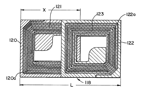
not been generally implemented. Fig. 4 shows a dual r~sonAnt
frequency cG~ Gaite security tag 118 in accor~ncD with a
first preferred embodiment of the present invention. The tag
118 is formed by ~ecuring together in a predetermined ~n~er a
first cecurity tag 120 ~nd a ~econ~ security tAg 122. The
first security tag 120 has a first resonant circuit including
a first inductor coil 121 and at least one capacitor. The
re~onAnt circuit of the first ~ecurity tag 120 has a first
predetermined resonant frequency.
W095/05647 ~ , PCT/US94/03864
-- 10 --
The ~econd security tag 122 also has A ~econd
resonant circuit formed of a 6econd inductor coil 123 and ~t
least one capacitor. ~he r~son~nt circuit of the ~econd tag
122 has a second predetermined resonant freguency which is
different from the fir~t predetermined resonAnt frequency of
security tag 120.
The first and ~Qcon~ security tags 120, 122 may be
~eparately formed utilizing ~ny known or traditional tag
fabrication techn;ques well known to those skilled in the EAS
art. After being fully separately formed, the two tags 120,
122 are secured together with the first inductor coil 121 of
tag 120 partially overlapping or overlying the ~econd inductor
coil 123 of tag 122 in a manner which ~;n;m; zes the magnetic
coupling between the inductor coils. More ~pecifically, the
tags 120, 122 are positioned with the coils 121, 123 partially
overlying each other ~o that the net flux generated from the
coil 121 of the first tag 120 is substantially zero within the
area of the coil 123 of the second tag 122 and the net flux
generated from the coil 123 of the second tag 122 is
substantially zero within the area of the coil 121 of the
first tag 120. When such a partial overlying of the inductor
coils exists, flux generated from current flowing through the
coil of one of the tags travels through the other tag in two
opposite directions. Properly positioning the tags with
respect to one another results in the flux generated by one
tag passing through the coil of the other tag in a first
direction being equal in magnitude to the flux generated by
the one tag passing through the coil of the other tag in the
opposite direction. Since the magnitudes of the flux passing
in the two opposite directions is equal or nearly egual, the
net flux flowing through the other tag as a result of the
current flow within the one tag is zero or near zero resulting
in the coupling between the tags 120, 122 being zero or near
zero. In this ~n~er, the tags 120, 122 function essentially
3~ independently of each other. Thus, two tags having two
different resonant frequencies may be positioned in close
~ W095/05647 ~7S PCT~S94/03864
-- 11 --
physical proximity to each other resulting in the tags being
physically effectively a single tag. Because ~f their close
proximity, signals received in the receiver 14 ~s A result of
the two tags 120, 122 being present within the detection zone
16 have essentially the same amplitudes thereby facilitating
more accurate tag detection than was possible with a ~ingle
tag 18 resonating at a ~ingle frequency.
The two tags 120, 122 may be secured together
utilizing a ~uitable adhesive or other means known in the art.
In the emboAi~?nt illustrated in Fig. 4, the tAgs 120, 122 are
oriented with the coil --ides facing in the ~ame direction and
with the capacitors located in diagonally opposite corners.
If desired, the tags could be in some other orientation, i.e.,
coil sides facing each other or coil sides facing away from
each other. Also, one or both of the tags 120, 122 could be
turned or rotated so that the capacitive lands ~re in a
different location with respect to each other either with the
tags in the illustrated orientation (i.e., both coil sides
facing the same direction) or in a different orientation.
Virtually any orientation or type of overlying relationship
could be employed. For example, the tags 120, 122 could be
turned ~o that only a corner 120a of tag 120 overlies a corner
122a of tag 122.
Figs. 5 ~nd 6 ~how a dual frequency tag 218 in
accordance with a second preferred ~ho~iment of the present
invention. Unlike the t~g 118 of Fig. 4 which was formed by
securing together two separate and in~epen~ent tAgs 120, 122,
tag 218 of the present embodiment is formed as a single tag
with two ~eparate resonant circuits which resonate at
different predetermined freguencies. Tag 218 includes a
single generally flat dielectric substrate 220 having fir~t
and second generally opposite principal surfaces. A first
resonant circuit including a first inductor coil 222
substantially located on the first surface of the substrate
and at least one capacitor formed o$ conductive lands 224, 226
on both sides of the substrAte 220 is formed in the usual
W095/05647 ~9~ PcT~S94/03864
- 12 -
manner. The first resonant circuit has a first predetermined
resonant frequency establi hed by the values o~ the r
inductor/capacitor. A ~econd rcron~nt circuit is formed of a
recon~ inductor coil 232 substantially located on the r?cQnA
5 principal surface of the substrate 220 and ~t least one
capacitor formed of conductive lands 234, 236 on both sides of
the ~ubstrate. The recon~ resonant circuit has ~ ~^cQn~
predeter~;~e~ resonant frequency establi~he~ by the ~alues of
the inductor/capacitor which prefer~bly is different from the
10 first predetermined resonant frequency in order to facilitate
separate and independent detection of the resonance of each of
the resonant circuits.
The key to forming the tag 218 is that the first
inductor coil 222 of the first resonant circuit is positioned
15 on the first principal surface of the substrate 220 so as to
partially overlie the second inductor coil 232 which is
positioned on the second principal ~urface of the ~ubstrate
220 in a manner which ri~;mizes the magnetic coupling between
the fi~st and cecond coils 222, 232. Proper positioning of
the inductor coils 222, 232 in an overlying manner results in
the net flux generated from one coil being zero or near zero
within the area of the other coil in the manner described
above with respect to the first embodiment.
The relationship between the inductor coils 222, 232
and the capacitor lands 224, 226, 234, 236 ~s ~hown in Figs. 5
2nd 6 is only for the purpose of illustrating the present
emboA; mPnt and may change, consistent with maintaining the
overlying relationship of the inductor coils 222, 232, if
desired. For example, the capacitor lands 224, 226, 234, 236
may be further spaced apart or may be pl~ced on diagonally
opposite corners. Thus, the specific orientation of the
components shown in the figures is not meant to be a
limitation upon the present invention. In addition, if
desired, each resonant circuit could comprise more than one
capacitor.~
W095/0s647 ~ PCT~S94/03864
- 13 -
In forming the tags 118, 218 of either of the above-
disclosed embodiments, the precise relationship between the
two inductor coils i5 a function of the specific geometry of
the inductor coils and any other elements which control or
affect the path of the magnetic flux. With the range of
possible coil geometries and other elements which affect the
path of the magnetic flux, for example, ron~l~ctive lands 234,
236 which, in conjunction with the dielectric, form the
capacitor of the resonant circuit, it is impossible to give a
precise formula for the amount of overlap that will result in
zero or near zero coupling between the inductors of the tags.
Howevert by example, referring to Fig. 4, which Chows the case
for two generally rectangulAr tags, the ratio of the
dimensions X/L generally falls between the range of 0.5 and 1.
Coil shapes which are generally not open and of a higher
degree of complexity may cause overlaps which are outside of
this range. In any case, the coupling between tags can be
measured by driving a first tag coil with a current and
measuring the induced voltage in a second tag coil as a
function of its position relative to the first tag coil. The
voltage induced in the cecond tag coil Chould be ~ini~ized by
moving the tags relative to each other to minimize the
coupling between the two tags.
Tags having two or more resonant frequencies in
accordance with either of the above-described embodiments may
be employed in connection with an existing EAS system 10 for
enhanced t2g detection. As long as each of the r~Fon~nt
frequencies of the t~g are within the range of the frequencies
~wept by the transmitter 12, no substantial modification need
be made to the transmitter 12. To enhance the ability of the
receiver 14 to discriminate between the multiple frequency t~g
and other signals within the surveillance zone 16, the
detection algorithms of the receiver 14 are modified to look
for each of the different resonant frequencies of the t~g; In
addition, the alarm enabling portion of the receiver is
modified so that an ~larm is not sounded unless the receiver
-
WO 95/05647 ~ PCT/US94/03864
-- 14 --
detects and verifies the simultaneous presence of a tag within
the detection zone 16 which is resonating at each of the two
or more predetermined resonant frequencies.
It ~hould be understood by those skilled in the art
that while the illustrated ~ho~ i ments of the present
~nvention are shown and described as being employed in an
electronic article security system 10, this is not meant to be
a limitation upon the present invention. Multiple frequency
security tags may be employed in many other types of systems.
For example, multiple resonant frequency tags may be used to
verify the identity of persons or objects or for establishing
the precise location of such persons or objects. As a
specific example, such multiple frequency security tags may be
secured to packages or luggage to establish the correct
routing or instantaneous location of such packages or luggage
using a frequency based detection system.
It will be appreciated by those ~killed in the art
that changes could be made to the embodiments described above
without departing from the broad inventive concept thereof.
For example, while the tags 118, 218 described above relate to
two resonant frequencies, it will be appreciated that each tag
may have more than two resonant frequencies. In addition,
while the tags 118, 218 as described ~re a particular type of
thin film tag, other types of tags which ~re fabricated in
other manners using other materials may also be employed as
multiple freguency tags. It is understood, therefore, that
this invention is not limited to the particular embodiments
disclosed, but it is intended to cover modifications within
the spirit and Ccope of the present invention as defined by
the appended claims.