Note: Descriptions are shown in the official language in which they were submitted.
2 i 70344
1
SIGNAL PROCESSING SYSTEM
This invention relates to processing signals received from a communications
channel. More particularly this invention relates to an integrated signal
processing
system for demodulating signals suitable for use in the transmission of
television
signals. w~~~---~~_~
~~q-Encoded transmission of inherently analog signals is increasingly
practiced today
as a result of advances in signal processing techniques that have increased
the bit rate
achievable in a channel. At the same time new data compression techniques have
tended to reduce the bandwidth required to acceptably represent analog
information.
Various modulation techniques have been employed in digital communications.
For
example quadrature amplitude modulation (QAM) is a relatively sophisticated
technique
favored by practitioners of digital radio communications. This method involves
two
separate symbol streams, each stream modulating one of two carriers in
quadrature. A
transmitted QAM signal can be represented by the equation
x(t) _ ~ cos(w~t) ~ Re{am}g(t-mT)
m=-m
- ~ sin(w~t) ~ Imam}g(t-mT)
m=_~,
wherein
am is a finite sequence of transmitted symbols;
g(t) is a real valued transmit filter; and
T is the symbol period.
As will be apparent to those skilled in the art this is equivalent to the
modulation of two
real-valued baseband pulse amplitude modulated (PAM) signals by the carrier
signals
cos (wit) and sin (w~t) respectively. As used herein the first term in the
above equation
is referred to as the "in-phase" component, and the second term is called the
"quadrature" component.
This system achieves spectral efficiencies between 5 - 7 bits/sec-Hz in
multilevel
formats such as 64- and 256-QAM. QAM is particularly useful in applications
having a
high signal-to-noise ratio. However double sideband modulation is required,
which
requires increased channel bandwidth for the same symbol rate over single or
vestigial
modulation schemes. Furthermore cross-coupled channel equalizers are generally
needed to cancel linear distortion in the channel, which adds to the overall
complexity
of the system.
A variant of QAM is quadrature phase shift keying (QPSK), in which a signal
2170344
2
constellation consisting of four symbols is transmitted, each having a
different phase
and a constant amplitude. The scheme is implemented as the sum of orthogonal
components, represented by the equation.
Am = be ~ em
where 8m can be any of ~0, rr/2, rr, 3n/2~. It is necessary to transmit both
sidebands in
order to preserve the quadrature information. The QPSK modulation scheme has
been
adopted by the ITU-T as an international standard for direct digital satellite
broadcasting.
In Europe 16-QAM and 64-QAM are used in the digital video broadcasting (DVB)
standard for digital cable broadcasting. Both QAM and QPSK have similar coding
schemes, which are generally described in Fig. 1 with reference to MPEG
transport
layer packets, wherein QPSK and QAM are implemented according to the standards
DVB-S (European Telecommunication Standard PrETS 300 421 ) and DVB-C (European
Telecommunication Standard PrETS 300 429) standards. MPEG is a standard well
known to the art, in which data is grouped in a plurality of packets, each of
which
contains 188 bytes. This number was chosen for compatibility with asynchronous
transfer mode (ATM) transmissions, another known telecommunication standard.
Various aspects of the coding process are specified in the respective DVB
standards,
including: randomization and sync inversion for synchronization; Reed Solomon
encoding; Forney interleaving; convolution encoding in the case of DVB-S, and
byte to
m-tuple mapping, and differential mapping in the case of DVB-C.
The art is presently striving to more efficiently transmit video and audio
data in
applications such as cable and direct satellite television using digital
techniques.
For a better understanding of these and other objects of the present
invention,
reference is made to the detailed description of the invention, by way of
example, which
is to be read in conjunction with the following drawings, wherein:
Fig. 1 is a block diagram illustrating QAM and QPSK coding and modulation;
Fig. 2 is a block diagram showing modulation and demodulation in a communica-
tion system;
Fig. 3 is a more detailed block diagram of the tuner and I,Q demodulator shown
in Fig. 2;
Fig. 4 is a diagram illustrating a portion of the modulator circuit shown in
Fig. 2;
Fig. 5 is a plot showing interpolated samples disposed between known samples;
Fig. 6 is a block diagram of a carrier recovery and a timing recovery circuit
in a
receiver according to the prior art;
Fig. 7 is a more detailed block diagram of the carrier recovery circuit shown
in Fig.
6;
2170344
3
Fig. 8 is a more detailed block diagram of the timing recovery circuit shown
in Fig.
6;
Fig. 9 is a diagram that illustrates the operation of the Gardner algorithm;
Fig. 10 is a block diagram of a carrier recovery and a timing recovery circuit
according to the invention;
Fig. 11 is a more detailed, partially schematic block diagram which
illustrates the
timing recovery circuit shown in Fig. 10;
Fig. 12 is a schematic illustrating a numerically controlled oscillator in the
timing
recovery circuit shown in Fig. 11;
Fig. 13 is a diagram illustrating the operation of the
circuit of Fig. 11;
Figs. 14a and 14b are plots of sinc pulses having different delay values which
are
helpful in understanding the operation of the circuits illustrated in Figs. 11
- 13;
Figs. 15a, 15b, 15c are plots which indicate the process of sinc
interpolation;
Fig. 16 is a schematic of a filter used in the sinc interpolator unit of the
circuit
shown in Fig. 10;
Fig. 17 is a schematic of a linear interpolation unit that can be used in the
circuit
of Fig. 10;
Fig. 18 is a schematic of a matched filter that is used in the circuit of Fig.
10;
Fig. 19 is a block diagram of a carrier recover circuit according to the
invention;
Fig. 20 is a block diagram of an adaptive phase tracking circuit that is used
in the
carrier recovery circuit depicted in Fig. 19;
Fig. 21 is an electrical schematic of the hopping adder used in the circuit
illustrated
in Fig. 19;
Fig. 22 is a block diagram illustrating a carrier recovery and a timing
recovery
circuit according to an alternate embodiment of the invention;
Fig. 23 is a more detailed diagram of a Hilbert filter used in the circuit
shown in Fig.
22;
Fig. 24 is a diagram illustrating constellation rotation error; and
Fig. 25 is a block diagram illustrating a second alternate embodiment of the
invention.
It is a primary object of the present invention to provide an improved signal
processing system for the communication of data in a constrained channel.
It is another object of the invention to provide an improved, economical
apparatus
for receiving and decoding data at high bit rates, such as video and audio
signals.
It is a further object of the invention to provide improved apparatus that
economically and reliably provide locking for the demodulation frequency
according to
21703-~
4
the modulator frequency in a communication system.
It is still another object of the invention to provide improved apparatus for
economically and reliably locking the data sampling frequency according to the
rate of
transmitted data in a communication system.
These and other objects of the present invention are attained by a signal
processing apparatus for processing signals that are sampled by a sampler
operative
at a sampling rate. The apparatus comprises a clock operative at the sampling
rate, a
first numerically controlled oscillator operative at periods T that are
initially equal to the
nominal baud rate of the signals, an interpolator, preferably a sinc
interpolator, receiving
samples at the sampling rate, and a loop filter coupled to the sinc
interpolator. The loop
filter has an output responsive to a difference between the periods T and a
received
symbol rate of the sampled signals. The first numerically controlled
oscillator is
responsive to the loop filter and generates an output signal that is
representative of an
interpolation distance between succeeding samples. The sinc interpolator
interpolates
the received samples according to the interpolation distance, and produces an
output
signal representative of the interpolated samples.
In an aspect of the invention the input signal is modulated, and the apparatus
further comprises an I,Q demodulator. First and second analog-to-digital
converters are
respectively coupled to an in phase output and a quadrature output of the
demodulator,
wherein the sinc interpolator accepts in phase and quadrature signals.
In another aspect of the invention the loop filter accepts an in phase
component
of the interpolated samples and the error signal is computed according to the
equation
error (r) = I r- 2 [I (r)+I (r-T)]
wherein I is the in phase component, T is the symbol period, and r is the
interval
between alternate samples.
In yet another aspect of the invention the loop filter accepts an in phase
component and a quadrature component of the interpolated samples the error
signal is
computed according to the equation
error(r) = I r- 2 [I (r)+I(r-T)J + Q r- 2 [Q (r)+Q(r-T)J
wherein I is the in phase component, Q is the quadrature component, T is the
symbol
period, and r is the interval between alternate samples.
In still another aspect of the invention the first numerically controlled
oscillator, the
sinc interpolator, and the loop filter comprise an integrated semiconductor
circuit,
170344
preferably a CMOS circuit.
The apparatus includes a matched filter which has an input coupled to the sinc
interpolator and an output coupled to the loop filter. Preferably the matched
filter is a
square-root raised cosine filter.
5 The output of the first numerically controlled oscillator comprises a first
output
signal that is generated whenever the state f2 exceeds a division of the
symbol period,
and the sinc interpolator generates an output in response to the first output
signal. The
output of the first numerically controlled oscillator includes a second output
signal that
is representative of a value D according to the equation
D = fraction 2 O MOD 1 system clock
2 baud rate
wherein system clock is the clock rate, baud rate is the nominal baud rate,
and f2 is a
state representative of a number of elapsed operative periods of the first
numerically
controlled oscillator, and the sinc interpolator emits an interpolated sample
upon
receiving the second output signal.
According to an aspect of the invention the sinc interpolator is a unit
comprising
a first sinc interpolator that receives an in phase component of the samples,
and a
second sinc interpolator that receives a quadrature component of the samples.
Preferably the sinc interpolator comprises a finite impulse response filter
having a bank
of coefficients.
In yet another aspect of the invention the bank of coefficients comprises a
plurality
of banks, and sinc interpolator is provided with an addressable memory
containing a
plurality of coefficients.
In another aspect of the invention the sinc interpolator performs a plurality
of sinc
interpolations that precede and follow a required sinc interpolation point,
and the
apparatus further comprises a linear interpolator that performs linear
interpolation on the
plurality of sinc interpolations.
The invention provides a circuit for processing modulated signals, comprising
a
semiconductor integrated carrier recovery circuit operative to control a
demodulator that
includes a second numerically controlled oscillator, and a digital derotation
circuit which
is responsive to the second numerically controlled oscillator and accepts an
in phase
component and a quadrature component of sampled signals. The carrier recovery
circuit
further comprises a phase error estimation circuit coupled to an output of the
derotation
circuit, and a loop filter coupled to an output of the phase error estimation
circuit,
wherein the second numerically controlled oscillator is responsive to the loop
filter.
1n a further aspect of the invention the circuit adaptively estimates the
phase error
2170344
6
and executes a least-mean-square algorithm. It comprises first and second
slicers which
accept a derotated in-phase value and a derotated quadrature value
respectively; first
and second subtracters for respectively determining first and second
differences
between the derotated in phase value and the sliced in phase value, and
between the
derotated quadrature value and the sliced quadrature value; and an angulator,
accepting the first and second differences and outputting a phase error
estimate.
Preferably the integrated circuit is a CMOS circuit.
The invention provides a signal processing apparatus for processing modulated
signals at a modulation carrier frequency, comprising a demodulator, a sampler
operative at a sampling rate on an output of the demodulator, and a carrier
recovery
circuit operative to control the demodulator in accordance with the modulation
carrier
frequency. The carrier recovery circuit comprises a second numerically
controlled
oscillator; a phase error estimation circuit; a digital derotation circuit
responsive to the
second numerically controlled oscillator and accepting an in phase component
and a
quadrature component of sampled signals; and a loop filter coupled to an
output of the
derotation circuit, wherein the second numerically controlled oscillator is
responsive to
the loop filter. The sampler and the carrier recovery circuit are integrated
in a
semiconductor integrated circuit, preferably a CMOS circuit.
In an aspect of the invention the carrier recovery circuit adaptively
estimates the
phase error according to the least-mean-square algorithm. It comprises first
and second
slicers which accept a derotated in-phase value and a derotated quadrature
value
respectively; first and second subtracters, for respectively determining first
and second
differences between the derotated in phase value and the sliced in phase
value, and
between the derotated quadrature value and the sliced quadrature value; and an
angulator, accepting the first and second differences and outputting a phase
error
estimate.
The invention provides a signal processing apparatus for processing modulated
signals that are sampled by a sampler operative at a sampling rate. The
signals have
a nominal baud rate. The apparatus comprising a clock, operative at the
sampling rate;
a first numerically controlled oscillator operative at periods T that are
initially equal to the
nominal baud rate; and a sinc interpolator receiving samples at the sampling
rate. A first
loop filter, coupled to the sinc interpolator and the first numerically
controlled oscillator,
has an output responsive to a difference between the periods T and a
transmitted
symbol rate of the sampled signals, wherein the first numerically controlled
oscillator is
responsive to the first loop filter and generates an output signal that is
representative
of an interpolation distance between succeeding samples, and the sinc
interpolator
interpolates the received samples according to the interpolation distance, and
produces
2170344
7
an output signal representative of the interpolated samples.
A carrier recovery circuit comprises a second numerically
controlled oscillator, a phase error estimation circuit, a
digital denotation circuit responsive to the second
numerically controlled oscillator and accepting an in phase
component and a quadrature component of sampled signals, and a
second loop filter coupled to an output of the denotation
circuit, wherein the second numerically controlled oscillator
is responsive to the second loop filter. The first and second
numerically controlled oscillators, the sinc interpolator, the
first and second loop filters, and the digital denotation
circuit are integrated in a semiconductor integrated circuit.
In one form of the invention an analog-to-digital
converter unit samples an input signal at the sampling rate
and has an output coupled to the sins interpolator. The
analog-to-digital converter unit is integrated in the
semiconductor integrated circuit.
In still another aspect of the invention the input
signal is modulated, and the apparatus further comprises an
1,Q demodulator, and a sampler comprising first and second
analog-to-digital converters respectively coupled to an in
phase output and a quadrature output of the demodulator,
wherein the sinc interpolator accepts in phase and quadrature
outputs of the sampler.
In accordance with the present invention, there is
provided a signal processing apparatus for processing signals
that are sampled by a sampler operative at a sampling rate,
-~--.-~.
74078-50
7a
the signals having a period corresponding to a received symbol
rate, the apparatus comprising;
a clock, operative at said sampling rate;
a numerically controlled oscillator operative at periods
T;
an interpolator receiving samples at said sampling rate;
and
a loop filter, coupled to said interpolator and said
numerically controlled oscillator and having an output
responsive to a difference between said periods T and said
period corresponding to said received symbol rate of said
sampled signals;
wherein said numerically controlled oscillator is
responsive to said output of said loop filter and generates a
first output signal that is responsive of an interpolation
distance between succeeding samples, and said interpolator
interpolates said received samples according to said
interpolation distance, and produces an output signal
representative of interpolated samples, and said numerically
controlled oscillator generates said first output signal
whenever a state S~ exceeds a division of said symbol period,
and said interpolator generates said output signal
representative of interpolated samples in response to said
first output signal, wherein S~ is a state representative of a
number of elapsed operative periods of said numerically
controlled oscillator.
In accordance with another aspect of the invention,
___.74078-50
7b
there is provided a signal processing apparatus for processing
an input signal having a period corresponding to a received
symbol rate, the apparatus comprising:
a clock, operative at said sampling rate;
a numerically controlled oscillator operative at periods
T;
a sinc interpolator receiving samples at said sampling
rate; wherein said interpolator comprises a finite impulse
response filter operable according to a bank of coefficients,
and an addressable memory having said coefficients memorized
therein;
a loop filter, coupled to said sinc interpolator and said
numerically controlled oscillator and having an output
responsive to a difference between said periods T and said
period corresponding to said received symbol rate of said
sampled signals;
a sampler, comprising first and second analog-to-digital
converters respectively coupled to an in phase component and a
quadrature component of said signals; wherein said sinc
interpolator and said loop filter accept in phase and
quadrature outputs of said sampler;
wherein said numerically controlled oscillator is
responsive to said loop filter and generates an output that is
representative of an interpolation distance between succeeding
samples, and said interpolator interpolates said received
samples according to said interpolation distance, and produces
an output signal representative of said interpolated samples;
74078-50
~~~'a~44
7c
and said numerically controlled oscillator, said sins
interpolator, and said loop filter comprise an integrated
semiconductor circuit, wherein said output of said numerically
controlled oscillator comprises a first output signal that is
generated whenever said state S~ exceeds a division of said
symbol period, and said interpolator generates an output in
response to said first output signal, wherein S~ is a state
representative of a number of elapsed operative periods of
said numerically controlled oscillator.
In accordance with another aspect of the invention,
there is provided a signal processing apparatus for processing
signals that are sampled by a sampler operative at a sampling
rate, the signals having a period corresponding to a received
symbol rate, the apparatus comprising:
a clock, operative at said sampling rate;
a numerically controlled oscillator operative at periods
T;
an interpolator receiving samples at said sampling rate;
and
a loop filter, coupled to said interpolator and said
numerically controlled oscillator and having an output
responsive to a difference between said periods T and said
period corresponding to said received symbol rate of said
sampled signals, wherein said loop filter accepts an in phase
component of said interpolated samples and an error signal is
computed according to the equation:
74078-50
~~~~~44
7d
error(r) - 1 Cr_T l[1(r) + 1(r-T)]
J2
wherein
1 is the in phase component
T is the symbol period; and
r is the interval between alternate samples;
wherein said numerically controlled oscillator is
responsive to said output of said loop filter and generates an
output signal that is representative of an interpolation
distance between succeeding samples, and said interpolator
interpolates said received samples according to said
interpolation distance, and produces an output signal
representative of interpolated samples.
In accordance with another aspect of the invention,
there is provided a signal processing apparatus for processing
signals that are sampled by a sampler operative at a sampling
rate, the signals having a period corresponding to a received
symbol rate, the apparatus comprising:
a clock, operative at said sampling rate;
a numerically controlled oscillator operative at periods
Ti
an interpolator receiving samples at said sampling rate;
and
a loop filter, coupled to said interpolator and said
numerically controlled oscillator and having an output
responsive to a difference between said periods T and said
74078-50
----._
7e
period corresponding to said received symbol rate of said
sampled signals;
wherein said numerically controlled oscillator is
responsive to said output of said loop filter and generates an
output signal that is representative of an interpolation
distance between succeeding samples, and said interpolator
interpolates said received samples according to said
interpolation distance, and produces an output signal
representative of interpolated samples wherein said loop
filter accepts an in phase component and a quadrature
component of said interpolated samples and said error signal
is computed according to the equation:
error(r) - 1 r_T [1(r) + 1(r-T)]
2
+ Q r-T [Q(r) + Q(r-t)]
2
wherein
1 is the in phase component;
Q is the quadrature component;
T is the symbol period; and
r is the interval between alternate samples.
In accordance with another aspect of the invention,
there is provided a signal processing apparatus for processing
signals that are sampled by a sampler operative at a sampling
rate, the signals having a period corresponding to a symbol
received rate, the apparatus comprising:
74078-50
CA 02170344 2000-12-O1
74078-50
7f
a clock, operative at said sampling rate;
a numerically controlled oscillator operative at
periods T;
an interpolator receiving samples at said sampling
rate, wherein said interpolator is a sins interpolator and
performs a plurality of sinc interpolations that precede and
follow a required sinc interpolation point;
a linear interpolator that performs linear
interpolation on said plurality of sinc interpolations;
a loop filter, coupled to said interpolator and said
numerically controlled oscillator and having an output
responsive to a difference between said periods T and said
period corresponding to said received symbol rate of said
sampled signals;
wherein said numerically controlled oscillator is
responsive to said output of said loop filter and generates an
output signal that is representative of an interpolation
distance between succeeding samples, and said interpolator
interpolates said received samples according to said
interpolation distance, and produces an output signal
representative of said interpolated samples.
In accordance with the present invention, there is
provided a signal processing apparatus for processing an input
signal having a period corresponding to a received symbol rate,
the apparatus comprising: a clock, operative at said sampling
rate; a numerically controlled oscillator operative at periods
T; a sinc interpolator receiving samples at said sampling rate;
wherein said interpolator comprises a finite impulse response
filter operable according to a bank of coefficients, and an
addressable memory having said coefficients memorized therein,
CA 02170344 2000-12-O1
74078-50
7g
wherein said sinc interpolator performs a plurality of sinc
interpolations that precede and follow a required sinc
interpolation point; a linear interpolator that performs linear
interpolation on said plurality of sinc interpolations; a loop
filter, coupled to said sins interpolator and said numerically
controlled oscillator and having an output responsive to a
difference between said periods T and said period corresponding
to said received symbol rate of said sampled signals; a
sampler, comprising first and second analog-to-digital
converters respectively coupled to an in phase component and a
quadrature component of said signals; wherein said sins
interpolator and said loop filter accept in phase and
quadrature outputs of said sampler; wherein said numerically
controlled oscillator is responsive to said loop filter and
generates an output signals that is representative of an
interpolation distance between succeeding samples, and said
interpolar interpolates said received samples according to said
interpolation distance, and produces an output signal
representative of interpolated samples; and said numerically
controlled oscillator, said sinc interpolator, and said loop
filter comprise an integrated semiconductor circuit.
The organization of a digital receiver 50 is shown in
Figs. 2 and 3. Although the invention is explained with
reference to a particular digital receiver, it will be
understood by those skilled in the art that it can be practised
in many forms of modulation and demodulation wherein it is
needed to accurately lock the demodulation frequency to the
modulation frequency. Similarly the teachings herein are
applicable to many systems wherein carefully synchronized
conversion of an analog signal to a digital signal is required.
CA 02170344 2000-12-O1
74078-50
7h
Fig. 2 illustrates a block diagram of a
communications system which includes a digital receiver 50. A
modulator 20 modulates and transmits a signal across a
communications channel 22, which is initially accepted by a
receiver front end 23, and demodulated in an l,Q demodulator
21. The demodulated signal is sampled in an analog-to-digital
converter ADC 60. Timing recovery is performed in timing
recovery circuitry 62. Carrier recovery is accomplished in a
carrier recovery circuit 64. The receiver typically includes
an automatic gain control (AGC) circuit 66. The sampled data
is processed through a matched filter 68, and is then subjected
to a slicer 69 and error correction circuitry 72, as discussed
below.
In the receiver front end 23, a radio frequency
amplifier 52 is coupled to the communications channel 22. The
channel is typically a constrained channel, such as a satellite
downlink, or a television cable, but can be any communications
channel. The output of the radio frequency amplifier 52 is
demodulated to a first intermediate
217344
~,,,, s
frequency by the first demodulator 24, and then passed through a band pass
filter 25.
The first demodulator 24 is of a known type. Its frequency is controlled by a
voltage-
controlled oscillator 33, programmed through a microprocessor interface 29
operating
through a digital-to-analog converter DAC 37. The intermediate frequency (IF)
signal
output from the amplifier 31 is demodulated in the I,Q demodulator 21 (Fig. 2)
to a
complex baseband representation using demodulator subunits 1, 2 included
therein, and
passed through low pass filters 3, 4 to produce the output signals Idata and
Qdata,
which are the in phase and quadrature components respectively. These signals
are
converted into a digital representation using a high speed analog-to-digital
converter unit
ADC 60.
The signal received from the channel 22 has been modulated as shown in Fig. 4.
Pulses comprising the in phase component Idata and the quadrature component
Qdata
are filtered through raised root cosine filters 5 and 6 respectively,
modulated on
orthogonal carriers at the carrier frequency w~ in multipliers 7, 8, and
summed in an
adder 9. Typically signals in adjacent passbands are transmitted along with
the desired
signal 10. In typical applications the excess bandwidth of the shaped pulses
exceeds
the Nyquist minimum by 35%. Optionally, the modulator may include an
intermediate
frequency (IF) stage (not shown). For a symbol period T of 33 ns, the Nyquist
frequency
is approximately 15 MHz, equivalent to approximately 30 MHz in the passband.
For
such a signal, a 40.5 MHz channel at 3 db rolloff would be required. The
adjacent
channels, channel distortion, and noise all must be considered in the design
of the
receiver and demodulator. The details of demodulation depend on the
communications
channel.
Referring again to Fig. 2, a high speed analog to digital converter, ADC 60,
provides an output which is used for timing recovery circuitry 62, which
insures accurate
sampling by ADC 60. In order to successfully recover the original data, the
receiver is
required to accomplish at least the following tasks:
(a) lock the demodulation frequency to the modulation frequency;
(b) lock the data sampling frequency to the transmitted symbol rate;
(c) adjust the gain of the tuner for optimal signal to noise;
(d) complete the pulse shaping to minimize intersymbol interference (ISI)
(e) perform a Nyquist filter operation to reject out-of-channel noise;
A carrier recovery circuit 64 controls the I,Q demodulator 21 such that the
correct
frequency and phase are recovered. The AGC circuit 66 feeds back to radio
frequency
amplifier 52. Both the AGC circuit 66 and the carrier recovery circuitry 64
are coupled
to the output of ADC 60. The main digital data stream from the ADC 60 is
filtered by a
matched filter 68, which precisely matches the characteristics of the transmit
filters (not
217~3~~
~"' 9
shown). A slicer 69 extracts the data from the filter output 68, determines
the nearest
legal constellation point, and applies a representation in appropriate format
to the error
correcting circuitry 72. The specification for the error correction is
specified in the DVB
specification, and will not be further discussed as it is outside the scope of
the invention.
Before proceeding to a further detailed description of the preferred
embodiment,
it is believed that the invention can be more clearly understood by comparison
to Figs.
6 - 9, which illustrate a conventional approach to the problems of carrier
recovery and
timing recovery. An off chip I,Q quadrature demodulator 10 is employed in the
tuner. An
external voltage controlled oscillator 42 is controlled by carrier recovery
circuitry block
44 in order to lock the demodulator clock to the frequency and phase of the
transmitted
signal. Typically the voltage controlled oscillator 42 can be adjusted across
a range of
several MHz. The sampling of the transmitted circuit is locked to the
transmitted symbol
rate and phase by an external voltage controlled oscillator 46, which is
typically a crystal
oscillator. The oscillator 46 is controlled by timing recovery circuitry 48,
but is generally
limited to a range of a few hundred KHz. Because different satellite
transponders and
cable television systems use different symbol rates, a plurality of voltage
controlled
oscillators (not shown) may be required to accommodate the diversity of
transmission
arrangements, or the device may be limited in its application to a particular
transmission
system. The demodulated data is sampled at T/2, the system clock rate in
analog-to-
digital converters 45, 47. At a symbol rate of 30 Mbaud, the system clock is
therefore
running at 60MHz. T/2 sampling is required for a Gardner timing recovery loop.
However
other circuitry outside the timing recovery loop is generally clocked a the
slower rate of
T to simplify implementation and reduce circuit area. After filtering in
matched filters 54,
56 the I,Q outputs 58, 59 are sent to a slicer and error correcting circuitry
(not shown)
as required by a particular application.
The matched filters 54, 56 are typically implemented as square-root raised
cosine
matched filters, having an excess bandwidth a = 0.35 to conform to the DVB
specification. These filters match a transmit filter (not shown) that was
employed in
transmitting the input signal so as to restore the signal to its
pretransmission character.
The carrier recovery circuitry 44 may be implemented as a conventional Costas
Loop, referenced generally at 61 in Fig. 7. After a channel change there may
be a
significant frequency error which has to be determined before phase can be
acquired.
A frequency-lock-loop of the type where the error signal 67 is proportional to
the
frequency error, or a frequency sweeping scheme can be used to determine the
initial
frequency error.
The timing recovery circuitry 48 is shown in more detail in Fig. 8. A
conventional
Gardner algorithm is employed, which acquires the timing sample point for T/2
sampling
2170344
by the AID converters 45, 47, and the units 55, 57. Even-numbered samples are
used
as data samples, while odd-numbered samples correspond to zero crossings. An
error
is computed according to the equation
5 error(r) = I r- 2 [I (r)+ I (r-T)] + Q r- 2 [Q (r)+Q (r-T)]
where
I is the in phase output;
Q is the quadrature output;
10 T is the symbol period;
r is the sample time of the even sample.
The Gardner algorithm is explained in greater detail in A BPSKlQPSK Timing-
Error
Detector for Sampled Receivers, Gardner, Floyd M., IEEE Trans. Comms, COM-34,
May 1986, pp. 423-9. Qualitatively, the error signal indicates the direction
the timing
sample point has to move in order to lock odd-numbered T/2 samples to the
midpoint
between samples, and to lock even-numbered sample points to the near optimal
sample
point. As the data is randomized in practical systems, there are an adequate
number
of zero crossings.
According to the algorithm the difference is calculated between a succeeding
even-numbered sample and a preceding even-numbered sample in subtracters 38,
39.
This difference is multiplied in multipliers 41, 43 by the odd-numbered sample
therebetween. The case where the sample point is too early will be explained
with
reference to Fig. 9. In the case of a falling edge 70, the intermediate odd-
numbered
point 71 has a positive value. The difference between the even-numbered points
73, 74
is negative, because the succeeding point 73 is closer to the zero line than
the
preceding point 74. Thus the product has a negative value. For a rising edge
80, the
odd-numbered intermediate point 78 has a negative value. The difference
between the
succeeding even-numbered points 82, 84 is positive. Thus the product also has
a
negative value.
A similar analysis reveals that in the case of late sampling, the Gardner
algorithm
yields a positive value in both rising and falling edges. In the interest of
brevity it will not
be repeated.
The error value indicates in which direction the sample point must move to
align
it correctly.
When the sample point is correct, the error value reported by the Gardner
algorithm is zero, except for noise and inter-symbol interference (ISI)
effects. However
the noise effects have a zero mean.
2~ ~~3~4
11
After processing, the even-numbered samples are sliced to give the
reconstructed
data which is applied to the error correcting circuitry. The odd-numbered
samples are
discarded before derotation. Of course it is equally possible to slice the odd-
number
samples and discard the even-numbered samples with appropriate modifications
of the
timing recovery circuitry. Similarly, sampling at other divisions of T could
be employed.
Although locking with odd-numbered samples at the zero crossing points does
not
guarantee that the optimum sampling point has been found for the data, the
scheme
works well in practice. Alternative schemes which more closely lock onto the
point
having a maximum likelihood of correctness could be used, but these are
generally
more complicated to implement.
The logic in the timing recovery circuit 48 operates at T, because an error
estimate
is generated only every other sample. However it requires two T/2 cycles for
an even-
numbered sample to propagate to the next even-numbered position in the shift
registers
63, 65, 75, 77 (Fig. 8). Thus the samples are clocked through at T/2.
A preferred embodiment of the invention will now be explained initially with
reference to Fig. 10. It has an advantage over the conventional circuit
discussed above,
in that the carrier and timing loops have been implemented entirely within the
digital
domain, and are integrated on a CMOS chip. As a result external system
component
costs are reduced. A further advantage of the arrangement is that the
demodulator can
work at many different symbol rates, or with variable symbol rate technology.
As
discussed above, the prior art solution required the variable crystal
controlled oscillator
to match the symbol rate.
A conventional off chip I,Q baseband demodulator 140 is employed. A suitable
I,Q quadrature baseband demodulator is the GEC Plessey SL1710 I,Q demodulator.
The external sample timing recovery loop has been replaced by a fixed
frequency
system clock 120, which clocks the logic. It must at least equal the data
Nyquist
frequency, or otherwise ensure that the data Nyquist frequency is met. An on-
chip
interpolator unit 130, which, under control of the timing recovery loop 125,
generates
synchronous T/2 spaced sample value. At each system clock tick, either one or
zero T/2
samples are generated by the interpolator unit 130. In the event that a sample
has been
generated, subsequent hardware modules are so informed by the assertion of a
"valid"
control strobe 170 (Fig. 11).
The external carrier recovery loop illustrated in Fig. 6, including the
external
voltage controlled oscillator 46, has been replaced with a fixed frequency
external
crystal oscillator 145. The oscillator 145 cooperates with an on-chip digital
derotater 150,
and an on-chip carrier recovery loop 155. Both the derotater 150 and the
carrier
recovery loop 155 are operative with T-spaced samples. The I and Q outputs
152, 154
2170.44
12
are applied to the slicer and error correction circuits in accordance with the
DVB
specification.
Timing Recovery
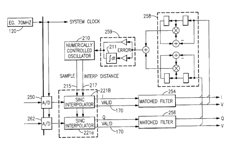
The timing recovery circuit according to the invention is shown in greater
detail in
Figs. 11 and 12. Quadrature demodulated data is sampled at the system clock
rate,
which, as explained above, must be at least equal to Nyquist frequency of the
input
data. As illustrated in Fig. 12, an on-chip numerically controlled oscillator,
shown
generally at 210, keeps count of symbol time. The state f2 of the numerically
controlled
oscillator 210 represents a fixed point count of the number of symbol periods
which
have elapsed. At each system clock tick, the state f2 increments by a value in
a register
260 equal to the (nominal baud rate / system clock rate), adjusted from the
nominal
using a control signal 262. The reciprocal of the value in the register 260 is
taken in a
reciprocal generator 240. The reciprocal is multiplied by the value [(21:x)
mod 1 ] / 2 in a
multiplier 241, and limited to a value that is less than 1 in saturation block
242.
Referring now to Figs. 11 and 13, an example is shown that illustrates the
operation of the circuit shown in Fig. 11, wherein the (nominal baud rate /
system clock
rate) = 0.4. Whenever the state !:2 passes a T/2 mark, indicated by the lower
row of
upward directed arrows in Fig. 13, the numerically controlled oscillator 210
outputs a
signal 215, and a value 0 217 which represents an interpolation distance
between
successive samples given by
D = fraction 20MOD 1 system clock
2 baud rate
The signals 215, and O 217 are accepted by a sinc interpolator unit 222,
comprising an
individual sinc interpolator 221a, 221b for each of the in-phase and
quadrature
components. The interpolator unit 222 then generates a sample value based on
the
interpolation distance. D has a value greater than or equal to 0 and less than
1, but is
represented as a fixed point number. Values greater than or equal to 1 are
saturated to
just less than 1. D can occasionally evaluate to greater than 1 when the
control signal
is positive. Under these conditions the value is limited to just under 1. The
sinc
interpolator unit 222 is instructed to generate a leading or a lagging sample
according
to whether D is 1 or 0 respectively. The spread of sample times covered by the
interpolator is one system clock period.
The numerically controlled oscillator 210 operates in a timing loop based on
the
Gardner algorithm discussed above. Other timing recovery algorithms may also
be
used, such as the Muller and Muller algorithm. A second order loop filter 259
is used.
A proportional-integral (PI) controller 211 is included in the circuit. Its
proportional and
217344
13
integral gain constants are selected to give the required damping factor and
natural
frequency. Preferably a relatively high natural frequency is used for initial
channel
acquisition in order to minimize lock time and insure acquisition. Thereafter
the
coefficients are changed to reduce the loop bandwidth and thereby make it less
sensitive to noise and fluctuations. This "gear shifting" operation improves
the overall
system bit error rate.
The matched filters 254, 256, preferably square-root raised cosine matched
filters,
are included because the Gardner algorithm assumes data having no ISI. They
cannot
be placed before the interpolator unit 222 because they have hard-wired
coefficients
designed for T/2 sampled data. As discussed above, the Gardner algorithm locks
the
timing sample point using T/2 samples. The loop preferably acquires the sample
point
such that odd samples are at the zero crossing points of the input data, and
the even
samples are used as data samples.
A delay is imposed between the presentation of system clock rate samples to
the
sinc interpolator unit 222 and the appearance of interpolated samples,
according to the
following equation
delay = D + ka
where
a = (system clock period / N);
N is the number of sinc interpolation points;
k = (integer) interpolation distance, ~N; and
D = constant delay implicit in hardware.
The sinc interpolator unit 222 is based on a finite impulse response filter,
which is
clocked at the system clock rate, with the coefficients being selected from a
bank of N
sets, wherein each set of coefficient interpolates a different delay. The
interpolation
distance output from the numerically controlled oscillator 210 determines
which bank of
coefficients are used to generate a given sample, as O varies from 0 to 1.
This can be
appreciated with reference to Fig. 5, wherein the oval indicators represent
interpolation
possibilities. Sinc interpolation is based on the sampling theory which shows
that a
signal which has been Nyquist sampled can be reconstructed using sinc pulses,
equivalent to performing a low pass filtering operation in the frequency
domain. The
output is given by the equation
y(t) _ ~ x (kT ) sinc n(t-kT )
k=-~ T ,
Referring to Figs. 15a - 15c, it will be seen that the reconstructed waveform
580
is the sum of all the components, representatively shown as lines 582, 584,
and 586.
14 2170344
There is only one non-zero component at each sample point, as shown in Fig.
15b. To
make implementation possible, i.e. to make the system causal, the tails of the
sinc pulse
have to be trimmed. This introduces negligible error. In order to interpolate
the value of
the signal at a point between known samples, it is necessary to sum the
contribution
made at that point by each known sample. The contributions are calculated
based on
the amplitude of the samples and the shape of the sinc pulse. The FIR filter
250 (Fig.
16) is used to calculate and sum the contributions. The coefficients of the
filter 250 are
calculated based on a system clock rate sinc pulse.
As shown in Fig. 16, the finite impulse response (FIR) filter 250 has a
plurality of
multipliers 252, each having a small read only memory (ROM) 251. The
multipliers 252
operate in parallel. Only the ROM 251 for the left-most multiplier 252 is
shown for clarity,
it being understood that each multiplier is operatively associated with a ROM.
Many
forms of memory could alternatively be used. For example in certain
applications it may
be desirable to operate the receiver under control, of a microprocessor (not
shown) and
the memory ROM 251 could be realized as a RAM, with programmable values.
Microprocessor interfaces for sampling receivers are well known, and will not
be further
discussed herein. The coefficients for each delay phase is stored within the
ROMs 251,
and an appropriate coefficient is selected in the ROM 251 by addressing logic
249
according to the interpolation distance provided by the numerically controlled
oscillator
210. The addressing arrangement for the ROMS 251 is conventional. The filter
250
includes a shift register 257 having plurality of tapped positions 258.
The coefficients that are stored in the ROMs 251 are based on a system clock
rate
sinc pulse. The zero delay coefficients have the sinc pulse centered at zero,
and model
the latest signal arrival when D = 0. The maximum delay coefficients
correspond to a
sinc pulse centered at (N - 1 ) / N system clock periods and are used whenever
O > (N -
1)/N.
Raised cosine sinc pulse coefficients, preferably with a = 0.35, are generated
using the general formula
sin T ~ cos aT x
c(x) = nx 2ax
T 1 _~ T
where
x=cT. n~T~
N
15 2170344
and
c is the coefficient number (e.g. -2, -1, 0, 1, 2);
n is the interpolation distance O...N-1.
The tap values for a 6 tap, 8 phase interpolator are given in the following
table.
Row 8 is not implemented.
Table 1
6-tap, 8-phase interpolation - FIR filter coefficients
bank D co c, c2 c3 c4 cs
(n)
0 0 s D < 0.1250 0 1.000 0 0 0
1 0.125 s O 0.033 0.093 0.974 0.127 0.042 0.014
< 0.250
2 0.250 s D 0.053 0.150 0.895 0.281 0.089 0.030
< 0.375
3 0.375 s D 0.061 0.171 0.772 0.450 0.132 0.046
< 0.500
4 0.500 s D 0.057 0.163 0.619 0.619 0.163 0.057
< 0.625
5 0.625 s D 0.046 0.132 0.450 0.772 0.171 0.061
< 0.750
6 0.750 s D 0.030 0.089 0.281 0.895 0.150 0.053
< 0.875
7 0.875 s D 0.014 0.042 0.127 0.974 0.093 0.033
< 1.000
8 not used 0 0 0 1.000 0 0
The data generated by the multipliers 252 are summed in an adder unit 253 and
output as interpolated data.
The operation of the sinc interpolator unit 222 can be further appreciated
with
reference to Figs. 5, 14a, 14b and 15a - c, wherein two exemplary delays
apply. For the
examples it is assumed that the interpolator has a 6-tap filter and 8 phases.
In actual
practice the number of taps and phases are selected according to the
application and
fhe resolution desired. In Fig. 14a, the coefficients for Bank 0 is shown.
Only the center
tap coefficient is non-zero. Thus the output data is based solely on the
contents of the
analog-to-digital value in the position 255, multiplied by a value memorized
in its
associated ROM (not shown). In Fig. 14b a longer delay is involved, and bank 7
of the
banks 0 - 8 has been selected, with the coefficients as shown. For example the
coefficient of the center tap has a value of 0.974. Interpolation makes use of
the known
sinc pulse shape of the received data.
Preferably the numerically controlled oscillator, sinc interpolator, and the
loop filter
~"" 2170344
16
comprise an integrated semiconductor circuit, which may be a CMOS circuit.
The accuracy of interpolation in the unit may optionally be increased by
incorporating a level of linear interpolation, as shown in Fig. 17, which
illustrates a linear
interpolation unit 267. This performs linear interpolation on sinc
interpolated values. As
shown in Fig. 5, a required interpolation point 261 is bracketed by preceding
and
succeeding sinc interpolation points 265 and 263 respectively. Linear
interpolation to
determine the value of point 261 is performed based on the points 265, 263. In
Fig. 17
a = (system clock period / N);
N is the number of sinc interpolation points;
k = (integer) interpolation distance, ON;
D = constant delay implicit in hardware; and
f = (fraction) interpolation distance, ~N.
Each system clock sample is sinc interpolated at interpolation points k, and k
+ 1
in sinc interpolation units 266, 268. The interpolation results are multiplied
by 1-f, and
f in multipliers 269, 264 respectively, and the result combined in an adder
270. An
interpolated sample value is output.
Referring to Figs. 11 and 18, the matched filters 254, 256 are implemented as
finite impulse response filters, and are enabled by the valid signal, Strobe
170, that is
generated by the interpolator unit 222. An exemplary filter 290 is illustrated
in Fig. 18.
Operation of the shift register 280 is enabled with the valid signal 170. One
output
sample is generated for each valid input sample. The FIR coefficients co..c~
are
calculated for a T/2 FIR square-root raised cosine filter assuming an excess
bandwidth
a = 0.35. The use of the valid strobe signal 170 emulates clocking with a
system clock
of T/2, although within the filter hardware is actually being clocked at a
faster rate, that
of the system clock 120 (Fig. 10).
Carrier Recovery
The carrier recovery loop is explained initially with reference to Figs. 19
and 20,
which illustrates a Costas algorithm phase error estimation section 315, a
second order
loop filter 320, a numerically controlled oscillator 310, and a digital
derotation circuit 317.
This circuit tracks any frequency errors and phase drift in the external
modulation and
demodulation chains. Preferably an additional adaptive loop circuit 319
operates
according to the least-mean-square (LMS) algorithm to adaptively estimate
demodula-
tion phase noise errors caused by hum and fitter.
Sin a and cos a control the derotation circuit 317. They are generated by use
of a
look-up table stored in a ROM (not shown). The design of trigonometric look-up
tables
is well known.
The derotator rotates the input data by 8. Given that (I,Q) represents a
vector of
217a3~~
17
amplitude (12 + Q2), and argument tan-'(I/Q) = cp. Thus I = sink and Q = cosh,
and we
require derotated I = I' = sin( + e) and Q' = cos(cp + 8).
I' = sink cos9 - cosh sing = I cos8 - Qsin9;
and
Q' = Qcose + I sine.
This is implemented in the network of multipliers and adders shown in the
derotation
circuit 317. The Costas phase error estimation section 315 completes the loop.
The derotator 317 in cooperation with the phase estimation section 315 is also
used to correct phase noise and fitter. This fitter is tracked by an LMS
adaptive estimate
of the phase error. Referring to Fig. 20, the derotated I and Q values,
represented as
fixed point numbers with a fractional part are sliced in slicers 332, 334
respectively to
the nearest legal constellation value. For QPSK this will be +1 or -1. The
difference
between the derotated value and the sliced value is obtained in subtracters
336, 338,
and forms the error. The I and Q error values are converted into a angular
error estimate
8 error. In the case of QPSK modulation, the 8 error is obtained from a
switching
network contained in angulator 331, according to table 2 below. The output of
the
angulator 331 is an adapted LMS estimate of the phase fitter or hum error 8
estimate.
The phase error estimation circuit disclosed in our copending application,
Ser. No.
08/481,107, incorporated herein by reference, can also be used, as may many
other
phase error estimation circuits, for example a circuit embodying the Costas
algorithm.
The LMS algorithm and its sign variant is well known, and will not be further
explained herein. It is discussed, for example, in Digital Communication,
Second Edition,
by Edward A. Lee and David G. Messerschmitt, Kluwer Academic Publishers, Chap.
11.
The adaptive algorithm has been modified slightly from the standard LMS
algorithm in that the 8 estimate has been given a leak. Normally leak is zero,
but every
Nth cycle it is -(sign(6 estimate)). This prevents the a error from growing
beyond
operational limits.
The Costas loop locks with the constellation points on the axis - i.e., (1,
0), (0, 1),
(-1, 0), (0, -1). Thus the error, in the example given, as shown in Fig. 24,
may be
estimated as 8error = sin-' (terror), which approximates to 9error = terror.
Similarly for
the other constellation points 8error is either + or - terror or Qerror as
shown in the table
below. A geometric representation of 8error is shown in Fig. 24.
Table 2
Approximation of 8 error
_Constellation A error
Q=1 __ I=0 terror
Q=0 I=1 -Qerror
217344
18
Q=-1 I=0 -terror
Q=0 I=-1 Qerror
Error calculation for QAM modulation schemes is more complicated.
As in the case of the timing recovery control loop disclosed hereinabove, the
proportional and integral gain constants PI controller 321 in the second order
loop 320
start off with wide bandwidth values to minimize acquisition time, and are
shifted to a
lower bandwidth loop set of values to optimize system bit error rate once lock
has been
achieved. The values selected can be readily selected in accordance with the
requirements of a particular application.
After a channel change there may be a significant frequency error which has to
be
determined before phase can be acquired. It preferable to implement a
frequency-lock-loop (i.e., one where the error signal is proportional to the
frequency
error) or a frequency sweeping acquisition scheme to be able to acquire the
initial
frequency error. A circuit that achieves a lock is explained with reference to
Fig. 21,
which is associated with the frequency and phase lock loop circuit 321,.
Should the
proportional integral loop 320 be unable to lock onto the frequency of the
received
intermediate frequency signal, the circuit of Fig. 21 allows the numerically
controlled
oscillator 310 to "hop" from one frequency to another at discrete intervals to
search for
the carrier of the incoming signal. The higher-order bits of the output of the
PI controller
321, referenced 458 in Fig. 21, are combined with a hop input 450, taken from
a state
machine 461, and submitted to the hopping adder 414. The adder 414 outputs a
frequency offset signal 452 which is accepted by the numerically controlled
oscillator
310.
Second Embodiment
Many forms of modulation are known to the art which do not generate both the
in
phase and quadrature components upon demodulation. For example, vestigial
sideband
(VSB) modulation is achieved by amplitude modulating a pulsed baseband signal,
and
suppressing a redundant sideband of the amplitude modulated (AM) signal, in
order to
conserve bandwidth. Usually the lower sideband is suppressed. In the digital
form of
VSB, a digital pulse amplitude modulated (PAM) signal is employed. The
alternate
embodiment of the invention disclosed hereinbelow with reference to Fig. 22 is
suitable
for the reception of VSB signals, as well as many other modulation schemes. As
in the
first embodiment, the output of an analog-to-digital converter 560 is applied
to a sinc
interpolator unit 522, which is followed by a matched filter 552, and a timing
recovery
circuit 525. The details of these components are the same as for the first
embodiment,
and need not be repeated. The derotation circuit 550, and the carrier recovery
circuit
555 have the same structure as in the first embodiment. However the derotater
circuit
2170344
19
550 requires a quadrature input, which must be generated, as it is lacking in
the
sampled demodulated signal that is output by the analog-to-digital converter
560. It is
possible to operate the timing recovery circuit 525 in accordance with the
Gardner
algorithm with only the in phase component, in which case the error signal
given above
will be
error (r) = I r- 2 [I (r)+I (r-T)]
where
I is the in phase output;
T is the symbol period; and
r is the sample time of the even sample.
The Q input is developed by a Hilbert filter, shown in Fig. 23. The Hilbert
filter has
an impulse response and a transfer function given by
h(t) - 1
nt
H(j,w) = jsgn(w)
The Hilbert filter is an eleven tap FIR filter, which has been implemented in
much
the same way as the FIR filter 290 (Fig. 18). The filter is organized as a
plurality of cells
operating in series, according to the length of the filter. One cell 782 is
illustrated in Fig.
23, it being understood that the other cells are structurally identical. In
order to reduce
hardware, the multiplier 786 is shared among the coefficients and the taps in
a data shift
register 783.
The multiplier-accumulator unit 705 of the cell 782 will be described. The
data shift
register 783 comprises registers 711, 712, 713, and 714, and is clocked at T,
which by
way of example is 133 ns. The outputs from the shift registers 710-713
therefore only
change only every 133 ns. The cell 782 could be implemented by associating a
multiplier with each of the registers 710-713, for a total of 4 multipliers.
However
because the multiplier 786 can operate in only 33 ns, T/4 the cell has been
designed to
have one multiplier 786 which is switched by switch 710 between the four data
registers
711-714. Four coefficient registers 720-723 are provided to supply the
multiplier 786.
Of course it is also required that the coefficient registers 720-723 also be
switched,
indicated by switch 724 in Fig. 23. The filter structure requires that the
cell output be
formed according to the equation
3
CCout = ~ ~nCn
n=0
20 217034
where
CCo~, is the cell output;
D~ is the contents of the nth data shift register; and
C~ is the contents of the nth coefficient register.
CCo~t is accumulated using the adder 726. The individual outputs CCo~t of each
of the
units 705 is latched, and summed in an adder tree 727. As the multiplier
requires the
largest area of each cell, a large amount of chip area has thus been
conserved.
Third Embodiment
A third embodiment of the invention is disclosed herein with reference to Fig.
25.
Its construction is similar to the first embodiment. However, having reference
to Fig. 10,
which has been discussed in connection with the first embodiment, it will be
noted that
the derotater 150 is disposed following the matched filters 254, 256. This
arrangement
has the advantage of using relatively inexpensive hardware in the derotator,
which can
be clocked at T. However the signals applied to the matched filters 254, 256
are
affected by constellation rotation and frequency errors, and hence the
filtered output will
not perfectly restore the source pulses. In Fig. 25 the derotater 652 is
disposed
intermediate the interpolator 622, and the matched filters 754, 756. The
derotater 652
is now required to be clocked at T/2; however the signal produced by the
matched filters
754, 756 is a more accurate restoration.
While this invention has been explained with reference to the structure
disclosed
herein, it is not confined to the details set forth and this application is
intended to cover
any modifications and changes as may come within the scope of the following
claims: