Note: Descriptions are shown in the official language in which they were submitted.
W~ 95/23472 PCT/US95/02257
2~ 7~7~4
HIGH SPEED DIFFERENTIAL RECEIVER FOR DATA
COr~lUNICATIONS
1. Field of the Invention
The present invention relates to the field of data
communications. More particularly, the present invention
relates to converting high speed differential serial
transmission signals to single-ended CMOS logic circuit
level signals.
2. Description of Related Art
It is well-known in the data communications field
that for the transmission of high bit rate data signals
small differential signals provide a number of advantages.
A differential channel provides rejection of common mode
noise present between a transmitting and receiving node
such as power supply noise. Differential signals can be
transmitted on twisted pair cables which are less
expensive than coaxial or fiber optic cables and which
when shielded offer very good rejection of interference
from external noise sources. Using small signal level
a
WO 95/23472 PCT/US95/02257
217 ~
2
differential signals on a shielded twisted pair cable
reduces EMI emissions, simplifies transmitter design and
reduces power dissipation. '
One of the most important characteristics of a
differential communication channel is that it reduces
offset or timing distortion due to mismatched rise and
fall times and receiver threshold. Timing distortion must
be minimized since in a digital communication system data
is encoded in both time and amplitude. Figure 1(a)
illustrates a single-ended system with mismatched rise and
fall times and a threshold VT. As can be seen the
mismatch in rise and fall times causes duty cycle
distortion (Tpulse does not equal Tb~ where Tb~ is the bit
cell width and Tpulse is the received pulse width.) It is
very difficult in a single-ended communication system to
match the rise and fall times and this mismatch becomes
significant when data rates become high (50 Mbaud or
more) .
Differential systems on the other hand do not suffer
duty cycle distortion due to rise and fall time mismatch.
As shown in Figure 1(b), as long as signal A and B have
equivalent rise times and equivalent fall times the
PCT/US95/02257
WO 95123472
3
signal's pulse width is preserved. This type of matching
is much more simple to guarantee in an integrated circuit
design that has a symmetric layout for the A and B
signals. It is also important to note that in a
differential receiver the threshold is not set externally
as in the single-ended system which was set by the VT
reference shown in Figure 1(a). Instead, the threshold in
a differential system is a function of the received signal
and therefore tracks with the received signal
corresponding to when A=B (the signal crossing point).
Circuits composed of CMOS digital logic generally
require signal swings having a range of 5 or 3 volts,
usually between +5 volts and 0 volts or +3 to 0 volts.
When a CMOS circuit receives a small amplitude
differential binary signal, it is necessary to convert the
binary differential signal into a single-ended signal
amplified to CMOS digital voltage levels usable by the
CMOS logic. As data transmission rates increase, it is
necessary that the signal conversion circuitry be able to
handle ever faster incoming differential signals for
conversion to digital levels.
WO 95/23472 PCT/US95/02257
4
It is desirable in many situations to implement a ,
signal receiver directly on the same integrated circuit
chip as many other digital logic circuits. Circuits
implemented on large digital chips generally operate from
a common power supply and are thus subjected to severe
power supply noise. In very large scale integrated
circuits, the power supply noise may be many times the
strength of the signal level of incoming signal
transmissions. This power supply noise can degrade or
totally obliterate the useful information in a received
signal.
In other technology areas it has been necessary to
convert signals from one domain to another domain. U.S.
Patent 4,437,171 illustrates circuitry for converting ECL
level signals to signals suitable for use by a MOS memory.
O 95/23472 PCT/US95/02257
2 l 70764
~~ARV OF THE IN~NTION
1
From the foregoing it can be appreciated that there
is a need for a serial data transmission receiver which
receives a high speed differential signal and converts it
to a single-ended signal at digital logic levels. It is
also desirable that such a receiver have a high bandwidth,
provide good common mode input signal rejection over a
wide common mode range and suffer minimal timing
distortion or offset. Further, such a receiver should
require a minimal amount of silicon die area and operate
with low power, low power supply voltages such as 3V, with
good power supply noise rejection.
These and other objects of the present invention are
provided by a differential-to-CMOS level signal conversion
apparatus which receives a binary differential input
signal having a small amplitude. The receiver can be
described as operating in two stages. The first stage is
the differential-to-single-ended conversion stage in which
the received differential signal is input into a
differential folded cascode transconductor. The
transconductor incorporates both P-channel and N-channel
cascade circuitry and a tail current transistor used to
WO 95!23472 PCT/US95/02257
2~7~764
6
bias an input transistor pair. Biasing voltages are
supplied by a biasing circuit that requires an external
reference current. The transconductor converts the
differential voltage inputs into a single-ended current
which is output into a tied-back inverter and a next
amplifying inverter. The combination of the differential
folded cascode transconductor, tied-back inverter and the
next amplifying inverter provide for very good power
supply noise rejection since the power supply noise is
coupled as a common mode signal input and rejected by the
equivalent circuit differential transconductor.
The second stage of the differential receiver circuit
is a series of CMOS amplifiers which first raise the
signal level of the first stage output to the desired CMOS
digital logic levels. The signal is also strengthened
through the chain of amplifiers. The inverter amplifiers
can be considered class AB amplifiers and have favorable
slew rates thus providing rapid signal rise and fall
times. Finally, the output of the second stage may be
driven through a tri-state bus driver for applications in
which the receiver is implemented on a bus.
CA 02170764 2003-11-20
7
Additional features of the receiver include on/off
switches which allow a disabled receiver to sit at either
a high logic level or a low logic level depending on
implementation. The high speed differential receiver
circuit of the present invention, if driven with 3-volt
power supply operates to produce 3-volt digital CMOS logic
levels and if driven with a 5-volt power supply produces
5-volt logic levels.
In one aspect, the present invention provides an
apparatus for converting a small amplitude differential
signal to a single-ended signal suitable for use in
digital logic circuits, said apparatus comprising: a first
stage circuit, the first stage circuit comprising a
differential transconductor to receive said small
amplitude differential signal, said first stage circuit
rejecting substantially all common mode input signal
received using said differential transconductor, the first
stage circuit further comprising a first stage amplifying
circuit coupled to the differential transconductor to
amplify an output signal of said differential
transconductor and to reject substantially all power
supply noise received, said first stage circuit converting
said small amplitude differential signal into a single-
ended signal, and a second stage amplifying circuit
coupled to said first stage circuit to amplify said
single-ended signal to digital logic signal levels.
WO 95/23472 PCT/US95/02257
9!
8
BRIEF DESCRIPTION OF TFiE DRAWINGS
The objects, features and advantages of the present
invention will be apparent from the following detailed
description in which:
Figures 1(a) and 1(b) illustrate graphically a
single-ended signal and a differential signal, comparing
characteristics of duty-cycle or timing distortion.
Figure 2 illustrates a block equivalent circuit of
the differential-to-CMOS converter and amplifier in
accordance with the present invention.
Figures 3(a), 3(b) and 3(c) provide an equivalent
circuit diagram for explaining some of the favorable
characteristics of the design of the present invention.
Figure 4 illustrates a transistor level diagram of
portions of the differential receiver circuit in
accordance with a preferred embodiment of the present
invention.
WO 95/23472 PCTIUS95/02257
217(776 r
9
Figure 5 illustrates a transistor level circuit
diagram of the biasing circuit used for driving the
differential receiver of the present invention.
WO 95/23472 PCTIZJS95/02257
~1~~~~4
DETAIT~ED DESCRIPTION OF TFiE INVENTION
A method and apparatus are described for the
conversion and amplification of high bandwidth, binary,
small amplitude differential serial data transmission
signals to single-ended digital CMOS level signals. In
the following description, many specific details are set
forth such as relative voltage levels and transistor
sizes, etc., in order to provide a thorough description of
the present invention. It will be appreciated, however,
by one of ordinary skill in the art that the present
invention may be practiced without such specific details.
In other instances, well-known structures and techniques
have not been described in detail in order not to obscure
unnecessarily the present invention.
The preferred embodiment of the present invention is
intended to be incorporated into a data bus receiving
module for use in a data communications system where
information is transmitted in serial binary format at a
very high rate of speed. Particularly, a preferred
embodiment of the present invention is intended to be
incorporated in a data communication system complying with
WO 95/23472 PCT/US95/02257
~ 2'~0~64
11
the IEEE Standard P1394, "High Performance Serial Bus"
wherein data is serially transmitted over a twisted-pair
cable from a transmitter on one node to a receiver on
another node. However, those of ordinary skill in the art
will see that the present invention may be implemented in
a wider field of use.
In light of the reasons discussed in the previous
section, it can be seen that it is desirable in high speed
serial transmission systems to use differential signals to
advantageously limit timing distortion and to reduce other
negative effects that are present when transmitting
single-ended signals. It is thus necessary to provide the
means for converting low voltage differential signals to
single-ended signals at digital logic levels for use by
digital circuitry. At very high speeds, and low voltage,
it is essential that the serial receiver provide good
common mode input signal rejection over a wide common mode
range as well as suffering very little timing distortion.
Likewise, it is desirable that the receiver require low
power and a small amount of silicon die area while also
providing good power supply noise rejection.
WO 95/23472 PCTIL1S95/02257
f
12
Referring now to Figure 2, an equivalent circuit of
the receiver of the present invention is illustrated. The
preferred embodiment receiver is intended to be
implemented in a system implementing the IEEE P1394, "High
Speed Serial Bus°' standard. This standard provides for
the transmission of serial data by means of a differential
signal over a twisted pair cable and exhibiting a peak-to-
peak swing of 300 millivolts. The small amplitude
differential signal, in order to be useful to digital
logic circuits must be amplified to either a 0 to 3 volt
range or 0 to 5 volt range for standard CMOS applications.
As illustrated in Figure 2, the differential receiver of
the present invention is shown having two salient stages.
The first stage 5 receives the small amplitude
differential signal from the twisted-pair coupling and
converts it to a single-ended signal with some
amplification. The second stage 10 receives the output of
the first stage and further raises the signal level to
CMOS digital logic levels and further increases the
strength of the signal. The output from stage two may be
used directly as the CMOS level digital signal, or the
output may be passed through a tri-state bus driver 12
WO 95/23472 PCT/US95/02257
2170764 ,
13
which couples the receiver to a bus 15 for conveying the
single-ended signal to the desired location.
The elegance of the present invention can be found in
the design of the first stage 5 of the differential
receiver. Bearing in mind that for a receiver to operate
at a very high speed on low amplitude differential
signals, the receiver must provide good common mode input
signal rejection over a wide common mode range while also
providing good power supply noise rejection. Accordingly,
the input to the receiver is a differential folded cascode
transconductor 20. It should be understood that the input
signal received by the transconductor 20 comprises two
components: the differential signal transmitted by a
transmitter with some biasing voltage at the other end of
the cable, and a common mode component which manifests
itself and is considered interference on the twisted-pair
cable. The differential signal has opposite values on the
two constituents of the twisted-pair cable, and thus the
differential components of the signal entering the two
inputs of the transconductor have opposite values. The
common mode signal picked up by the twisted-pair has an
equivalent value on both cables entering the receiver.
Because the receiver is a differential transconductor, the
WO 95/23472 PCT/US95/02257
2~~~~ 64
14
equivalent signals are canceled out and only the
differential signal is processed by the receiver circuit.
Using the differential transconductor 20 thus provides for
good common mode input signal rejection for the receiver.
For reasons that will be described further herein with
respect to the particular circuitry used to implement the
transconductor, the receiver of the present invention
provides good common mode rejection over a common mode
range of approximately 1.2 to 3.0 volts for a 3-volt CMOS
implementation and 1.2 to 5.0 volts for a 5-volt CMOS
implementation.
The output of the transconductor 20 is provided to a
first inverter 22 which is tied-back for self-biasing.
The signal is then inverted and further amplified by the
inverter 24 to complete the signal processing carried out
by the first stage 5 of the differential receiver of the
present invention. In the preferred embodiment, inverters
22 and 24 are the same size.
Because the differential receiver of the present
invention is designed to be implemented on highly
integrated circuits, it is important that the receiver
provide good power supply noise rejection. Power supply
WO 95123472 PCT/US95l02257
noise is inherently present in highly integrated
semiconductor circuits. In fact, the power supply noise
can be several times the size of the signal that the
receiver is supposed to be detecting. To this end, it
will be seen that the circuit design of the first stage 5
provides an elegant solution to the need for rejecting
power supply noise. This will be explained with reference
to Figures 3(a)-3(c). In Figure 3(a), it is shown that
the inverter 24 can be alternatively illustrated as a
differential transconductor 25 having a tied-back or self-
biasing inverter 27 coupled to one input. Upon careful
consideration, it will be understood by those of ordinary
skill in the art that these are equivalent circuit
representations wherein the inverter can be considered an
ideal transconductor with its threshold equivalent to the
threshold of an inverter having the same transistor size
ratio. Figure 3(b) illustrates that the differential
folded cascode transconductor 20 which receives the
differential input signal can be illustrated more simply
as a current source 21 that can source or sink current.
Thus, lfigure 3(c) shows an equivalent circuit to the first
stage 5 of the differential receiver of the present
invention.
WO 95/23472 PCT/US95102257
I
2~
16
The equivalent circuit shown in Figure 3(c) shows a
differential transconductor 25 which has at one input the
tied-back or self-biasing inverter 27 as well as the tied-
back or self-biasing inverter 22 which was described above
with respect to Figure 2 and is the same size as inverter
27. The current source 21 sources or sinks current
through one of these two inputs, shown being injected
through self-biasing inverter 22. As was described above,
it is only the differential inputs to a differential
transconductor that are processed while common mode input
signals are rejected. It can therefore be seen from the
equivalent circuit of Figure 3(c) that the first stage 5
portion of the differential receiver of the present
invention provides very good power supply noise rejection
since the power supply noise is coupled as a common mode
input signal through the two self-biasing inverters and is
rejected by the differential transconductor. This is true
even though inverters alone generally exhibit poor power
supply noise rejection. Only the differential signal,
which in this case is the injected current from the
current source 21, is yielded from the first stage 5 of
the differential receiver. It should be noted that to
facilitate this coupling of power supply noise as a common
PCT/US95/02257
O 95/23472 2 l 7 ~ ~ 6 4
17
mode input signal that the transistors utilized for the
inverters 22 and 24 should have the same transistor sizes.
Referring back now to Figure 2, it is now understood
that the novel circuit design of the first stage 5 of the
differential receiver provides for good common mode input
signal rejection over a wide common mode range as well as
providing good power supply noise rejection. The single-
ended output signal from the first stage 5 is next
propagated to the second stage of the differential
receiver, the amplifying stage 10. In this stage, the
single-ended signal is now propagated through a string of
inverters which serve to raise the single-ended signal to
CMOS logic levels and further amplify the signal to a
useful strength. It turns out that it is faster to use a
chain of inverters because a single larger inverter will
have the effect of slowing down the node. These inverters
are typical CMOS inverters comprising two transistors each
which can be processed efficiently by known technologies.
In a preferred embodiment implementation, inverters 26 and
28 utilize the same size transistors as inverters 22 and
24 while inverter 30 may be in the range of two to three
times that size and inverter 32 may have transistors twice
again the size of the transistors of inverter 30. It is
WO 95/23472 PCT/US95/02257
18
important in implementing the present invention, at least
for the preferred embodiment implementation, that the
inverters 22, 24, 26, 28, 30 and 32 all use transistors of
the same size and ratio, although for signal strengthening
as described, inverters 30 and 32 implement multiple
transistors. It will be understood that the inverters are
intrinsic class AB amplifiers which, once switched to the
rails do not use any power. This facilitates a low power
aspect in designing an efficient receiver in accordance
with the present invention. Likewise, the design provides
for a favorable slew rate yielding very fast signal rise
and fall times in providing a very high speed receiver for
serial data transmissions.
Those of ordinary skill in the art may envision
alternative circuitry for amplifying the output from the
first stage of the receiver. The output from the second
stage of the receiver circuit illustrated in Figure 2 may
directly be used to drive digital CMOS logic circuits, or
it may be passed through tri-state bus driver 12 for
coupling the receiver to a bus 15.
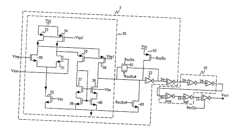
Referring now to Figure 4, a more detailed circuit
diagram of the differential receiver of the present
WO 95123472 PCT/ITS95/02257
2 ~ 707
b4
19
invention is illustrated. In this figure, the circuitry
for the differential folded cascode transconductor 20 is
illustrated at the transistor level. It can be seen that
the differential signal is inputted to the transconductor
through differential NMOS input transistors 50 and 51.
The sources of the two NMOS differential transistors 50
and 51 are coupled to the drain of tail current source
transistor 52 which has its gate coupled to a biasing
circuit to be described further herein with respect to
Figure 5. The tail current transistor 52 is used to
provide current flow in the differential input transistor
pair.
The differential folded cascode transconductor 20
further incorporates PMOS transistors 53, 54, 55 and 56
which are coupled together to provide a P-channel folded
cascode circuit. These transistors also receive their
biasing gate voltages from the biasing circuit to be
described further herein with respect to Figure 5.
Finally, NMOS transistors 57, 58, 59 and 60 are coupled
together to form the N-channel cascode current mirror
circuit. The biasing voltage Vbn to the N-channel cascode
circuit is also provided from the
WO 95123472 PCT/US95102257
r
biasing circuit to be described further herein with ,
respect to Figure 5. Those with an understanding of
circuit design will see that the N-channel and P-channel
cascode circuits are coupled in an arrangement such that
the current drawn through differential input transistors
50 and 51 is folded through the circuit and forced to
propagate to self-biasing inverter 22. Transistors 50
through 60 are biased in the saturation region. The
currents in transistors 53 and 54 are equal and are
typically about 25~ higher than the current in transistor
52. It should be understood that the polarities for the
transistors described above are chosen to suit the common
mode range of the preferred embodiment implementation.
Over a different common mode range, those of ordinary
skill in the art will appreciate that the differential
folded cascode transconductor 20 could be implemented with
the transistor polarities reversed (i.e., p-transistors
switched for n-transistors and vice versa).
The circuit diagram of Figure 4 also illustrates a
switch 61 being inserted within the circuit of the tied-
back inverter 22. The switch 61 should be sized such that
its transconductance gm is much larger than the gm of the
tied-back inverter 22. This is used for disabling the
WO 95/23472 PCT/US95/02257
2170764
21
receiver controllably based on an enable signal supplied
thereto. Because the inverters are intrinsic class AB
inverters which will draw no power once either fully in
the on or fully in the off state, the receiver should be.
implemented such that it exhibits a logic low signal
constantly or a high logic signal constantly when it is
off. There is shown in Figure 4 two switching
transistors, PMOS transistor 62 with its source tied to
Vcc and NMOS transistor 63 with its source tied to ground.
These are alternative transistors, with one providing the
output to be exhibited in a low state and the other
causing the output to be exhibited in a high state. By
implementing and turning on PMOS switching transistor 62
when the circuit receiver is disabled, the output from the
tied-back inverter 22 will be a CMOS low which results in
a low Vout because of the even number of inverters
present. Alternatively, by having present and turning on
NNiOS switching transistor 63, when the circuit receiver is
disabled, the output from the tied-back inverter 22 will
be CMOS high, resulting in a high output due to the even
number of inverters. Transistors 62 or 63 must be strong
enough to overcome the output current of the stage 20 and
WO 95/23472 PCTIUS95/02257
22
force the output of the inverter 22 to the appropriate
CMOS level.
In the preferred embodiment implementation of the
present invention, the transistor sizes for the circuit,
measured in microns, are as follows: for the differential
input transistor pair, the NMOS transistors have the
dimensions of 2 x 120/1.2. The P-channel cascode circuit
transistors 53, 54, 55 and 56 are all 60/1 and the NMOS
transistors 57, 58, 59 and 60 of the N-channel cascode
circuit are 30/1. Transistor 52 is 4 x 32/2.4. Finally,
if the PMOS switch 62 is implemented its dimensions are
8/0.8 while an NMOS switch 63 if implemented is 5/0.8.
For the inverters 22, 24, 26 and 28, the N-channel
transistors are 3/0.8 and the P-channel transistors are
6/0.8. Inverter 30 is sized with multiples of the other
inverters with the N-channel transistor being 2 x 3/0.8
and the P-channel transistor being 2 x 6/0.8. Similarly,
the N-channel transistor of inverter 32 is 4 x 3/0.8 and
the P-channel transistor is 4 x 6/0.8.
Referring now to Figure 5, the circuit implemented
for biasing up the differential folded cascode
transconductor 20 is illustrated. The biasing circuit -
requires an independent current source 70 which provides
WO 95/23472
PCT/US95/02257
r
23
25 ~.~.amps to NMOS transistor 71 in the preferred
embodiment. The NMOS transistor 71 operates as a switch
controlled by a receiver power-up which, when open
prevents current from flowing in the rest of the biasing
circuit. This also shuts down the current in the
transconductor circuit stage 20 as described above with
respect to Figure 4.
When the switching transistor 71 is closed, a current
from the current source is mirrored through the rest of
the circuit. The current is mirrored by PMOS transistors
72 and 73 and flows into diode-connected N-channel
transistor 74 which supplies the gate voltage to the N-
channel cascode circuit. The current also gets mirrored
at PMOS transistor 75 and flows into diode-connected N-
channel transistor 76 which sets up the bias voltage to
the tail current transistor 52 of Figure 4. The current
is then mirrored by NMOS transistors 78 and 77 which sets
up a current that flows through diode connected PMOS
transistor 79 and transistors 80, 81, respectively. This
sets up the bias voltage for the P-channel cascode circuit
described above with respect to Figure 9. The transistors
81, 82 and 84 are used as decoupling capacitors. The
transistor sizing for the preferred embodiment, in
WO 95/23472 PCT/US95102257
24
microns, is illustrated in Figure 5 using conventions
understood by those of ordinary skill in the art.
There has thus been described a method and apparatus
for the reception of high speed small amplitude
differential signals and the conversion of those signals
into single-ended digital logic levels. Although the
present invention has been described in terms of a
preferred implemented embodiment, it will be appreciated
that various modifications and alterations might be made
by those of ordinary skill in the art without departing
from the spirit and scope of the present invention. The
invention should, therefore, be measure in terms of the
claims which follow.