Note: Descriptions are shown in the official language in which they were submitted.
A DIGITAL OPTICAL SWITCH AND MODULATOR AND A METHOD FOR
DIGITAL OPTICAL SWITCHING AND MODULATION
BACKGROUND OF THE INVENTION
FIELD OF THE INVENTION
The present invention relates generally to optical switches and modulators,
and
more particularly to an electrode configuration for controlling the electric
field applied
to an optical waveguide in optical switches and modulators.
RELATED ART
Certain types of waveguide based optical switches, also referred to as optical
modulators, are receiving a great deal of attention due to their digital
optical output
characteristic. These waveguide based optical switches can be controlled
through the
electro-optic effect. The electro-optic effect is a term used to describe the
change in
the index of refraction of an optical waveguide that results from an electric
field applied
through the optical waveguide.
Changes in the index of refraction of an optical waveguide affect the
propagation of light through the optical waveguide. For example, a change to
the
index of refraction of an optical waveguide may direct light to propagate in
an optical
waveguide. Alternatively, a change in the index of refraction of an optical
waveguide
may direct light away from propagating in an optical waveguide. For a properly
designed switch, application of a control voltage, therefore, can cause the
optical
waveguide to exhibit a digital response function. That is, the optical output
power of
an optical waveguide yields a step-like curve when it is plotted against
increasing
control voltage, that is, there are no significant secondary maxima in such a
plot.
An advantage of a digital response characteristic is that the switch can be
set to
direct an optical signal to a given output waveguide without regard to the
polarization
of the input signal despite the fact that the electro-optic effect is
different for the two
polarizations. Another advantage of a digital response characteristic is that
the output
2
optical power of the optical waveguide is not sensitive to voltage variations
or drift in
the applied control voltage. Application of an appropriate control voltage
allows light
to be routed through a desired path of an optical switch. Routing light in
this manner is
called switching. When an appropriate control voltage is applied to each of
two output
waveguides, propagation of light is promoted in one of the output optical
waveguides
and propagation of light is inhibited in the other output optical waveguide.
Optical
switches have broad optical bandwidths making them attractive for the
switching needs
of high data rate transmission systems, including space- and time-division
multiplexing.
In addition, optical switches may find application in other areas such as
optical signal
processing. An optical modulator functions much the same as an optical switch
because the optical output power in either of the output optical waveguides
can be
modulated by an appropriate control voltage.
Optical switches have been implemented using x- or y-shaped optical
waveguides. A y-shaped optical waveguide consists of three optical waveguides:
one
input optical waveguide connected to two output optical waveguides. The input
waveguide is connected to the output waveguides at an optical waveguide branch
start
plane. An x-shaped optical waveguide consists of four optical waveguides: two
input
optical waveguides connected to two output optical waveguides. The input
waveguides connect to the output waveguides at an optical waveguide branch
start
plane. The terminology, "x-shaped" and "y-shaped", is used as a shorthand to
describe
the multiple waveguides which form an x-shaped or y-shaped optical waveguide
respectively. The terms are descriptive of the shapes of the resulting
waveguides.
Optical switches using an x- or y-shaped optical waveguide exhibit the highly
desirable
digital behavior described above. Thus, the voltage transfer characteristic of
optical
switches made using x- or y-shaped optical waveguides looks like a step
function.
X- and y-shaped optical waveguides may be manufactured using a birefringent
material such as lithium niobate (LiN03). A birefringent material causes
different
polarizations of light to behave differently when they propagate through it. A
light
beam that is propagating through a waveguide of an optical switch comprises
two
polarizations (see Figure 2A): a transverse magnetic polarization (TM) 202 and
a
transverse electric polarization (TE) 204. The two polarizations may be
defined
anywhere in the plane which forms a right angle to the direction of
propagation of light
through an optical waveguide. In the field of waveguide devices, axes are
conventionally defined with respect to the top surface of the crystal
substrate in which
the optical waveguide resides. Light with a transverse electric polarization
is defined as
light having an electric field vector parallel to the top surface of the
crystal substrate.
In TE polarized light 204, the magnetic field vector, which is perpendicular
to the
electric field vector, is perpendicular to the top surface of the substrate.
Likewise, light
with a TM polarization 202 is defined as light having a magnetic field vector
parallel to
the top surface of the crystal substrate in which the optical waveguides
resides. In TM
polarized light 202, the electric field vector, which is parallel to the
magnetic field
vector, is perpendicular to the top surface of the crystal substrate.
In order to obtain a digital response function for a polarization independent
switch, the power of both the TM and TE polarizations of light 202, 204 in a
waveguide of an optical switch must be reduced to as near zero as possible.
Figure 2A
shows exemplary optical transfer curves for prior art directional coupler
switches in z-
cut lithium niobate. In order to reduce the power of both the TM and TE
polarizations
of light 202, 204 to as near zero as possible, an increasing control voltage
must be
applied to the waveguide. Power in the TM polarization of light 202 approaches
zero
faster than the TE polarization of light 204 (this is apparent from Figure
2A). Therefore,
a greater control voltage must be applied to an optical waveguide to reduce
the power
in the TE polarization of light 204 to zero than need be applied to reduce the
TM
polarization of light 202 to zero. As greater voltage is applied to the
optical waveguide
to reduce the TE polarization 204 to zero, the TM polarization 202 rises (see
example
rise 206 in Figure 2A). The rise 206 in the. TM polarization of light 202
results in
crosstalk. Crosstalk refers to unwanted power which appears at the output of
one
optical waveguide when an electric field has been applied to the switch to
direct the
optical power to the other output optical waveguide. X- and y-shaped optical
waveguides are advantageous because they reduce the rise 206 in the power of
the TM
polarization of light 202 as the control voltage is increased (see Figure 2B).
Optical
~~ WJ
4
switches using x- or y-shaped designs, therefore, reduce crosstalk and signal-
to-noise
problems associated with other kinds of optical switches which do not use x-
or y-
shaped designs.
Typically, single mode optical waveguides are used in optical switches. A mode
refers to the distribution of the light across the width of an optical
waveguide. A single
mode optical waveguide has a width sufficient to support only a single mode of
light
propagating thorough it. The mode supported in a single mode optical waveguide
appears at the end of the waveguide as a single spot of light. In a multiple
mode
optical waveguide, the width of the optical waveguide is sufficient to support
multiple
modes of light. In a multiple mode optical waveguide, multiple spots of light
appear at
the output of the waveguide. In a single mode x- or y-shaped optical switch,
only one
mode of light is supported in the optical waveguide of the optical switch. An
exception
occurs where the x- or y-shaped optical waveguide begins to branch. Two modes
are
possible at this point because of the larger width of the waveguide where it
begins to
branch.
Switching occurs in the active region of an x- or y-shaped optical waveguide.
The active region of an x- or y-shaped optical waveguide begins in the region
where
the x- or y-shaped optical waveguide begins to branch (i.e., where the input
waveguide(s) connect to the output waveguides) and extends to the end of the
electrodes. Applying an electric field across the branches (the separation or
split in a x-
or y-shaped optical waveguide) of an x- or y-shaped optical waveguide changes
the
index of refraction in those branches (changing the index of refraction in an
x- or y-
shaped optical waveguide causes propagation of light in the branches of the x-
or y-
shaped optical waveguide to be inhibited or promoted). The electric field can
be
applied such that one branch of an x- or y-shaped optical waveguide promotes
propagation of light through it, while the other branch of an x- or y-shaped
optical
waveguide inhibits propagation of light through it. The branches of an x- or y-
shaped
optical waveguide are coupled. That is, the power of the light in the
inhibiting branch
of the waveguide is transferred to the light in the promoting branch such that
the
promoting branch contains all of the power of the original input light.
CA 02171120 1998-11-27
An x-switch provides more flexibility in switching than a y-switch because it
is a 2x2 switch whereas the y-switch is a 1x2 or 2x1 switch. A 2x2 switch has
two
inputs and two outputs. The flexibility of the 2x2 switch derives from its
ability to
route either input to either output. Because the x-switch is difficult to
design however,
5 the less flexible 2x 1 or 1 x2 y-shape design is more common. However, the
following
discussion about the design of the electrodes apply to an x-switch as well as
a
y-switch.
Digital optical switches have different electrode and optical waveguide
configurations depending on, among other things, the type of crystal substrate
from
which the electrodes are made. In lithium niobate, the largest electro-optic
effect is
obtained for electric fields which are parallel to the crystalline z-axis.
Thus, for optical
waveguides fabricated in x- or y-cut crystalline material, the electrodes are
placed on
the substrate surface adjacent to the waveguides. The waveguides and
electrodes are
oriented such that the applied electric field is primarily parallel to the
surface of the
substrate and in the z direction where it passes through the waveguides. For
optical
waveguides fabricated in z-cut crystalline material, the electrodes are placed
in a
plane, parallel to and distinct from a plane in which the waveguides are
located so that
the applied electric field is primarily perpendicular to the surface and in
the z
direction where it passes through the waveguides.
For digital switches, a first conventional electrode waveguide configuration
is a
two electrode design. The two electrodes follow the branching of the output
waveguides, resulting in a non-constant distance between electrodes as the
waveguides
branch. The effect of the non-constant distance along the length of the
optical switch
is that the electric field, which is proportional to applied voltage (V)
divided by the
distance between the electrodes at a particular point (L), decreases in
intensity as L
increases. Thus, the waveguides become inefficient very quickly as they
separate, that
is, as L increases. A further disadvantage of the first conventional electrode
configuration is that advantageous voltage-length reduction techniques, such
as one
CA 02171120 1998-11-27
6
described in W. K. Burns, "Shaping the Digital Switch," IEEE Photonics
Technology
Letters, Vol. 4., pp. 861-863, August 1992, cannot be applied because such
techniques
require the application of a constant electric field.
A second conventional electrode waveguide configuration uses a four electrode
design. This configuration maintains a constant separation between pairs of
electrodes,
thereby overcoming the problem of the V/L inefficiency, described above, for
the two
electrode design. However, this second conventional electrode configuration
suffers
from other problems. In particular, there is a practical limit as to how close
the inner
two electrodes can get. The limit is imposed by the resolution of modern
photolithographic processes used to create the electrodes. Further, arcing
across the
point of closest proximity (between the innermost 2 electrodes) becomes a
problem
when the electric field intensity is sufficiently high. Thus, the electrodes
do not extend
into the input region of the optical switch. Light propagating in the optical
waveguide
of an optical switch which employs the second conventional electrode
configuration,
experiences an abrupt change in the electric field applied to the optical
switch at the ,
beginning of the electrodes. An abruptly applied electric field results in
increased
crosstalk and propagation disturbance in the optical waveguide. Preferably,
the electric
field should be applied in a smoothly varying way so as to minimize crosstalk
and
disturbance of mode propagation.
Therefore, what is required is an optical switch having an electrode
configuration that overcomes the above-stated problems. The new electrode
configuration should apply a constant electric field through a substantial
portion of the
separation of the output branches (i.e., the branches through which light
propagates
after switching) of the optical waveguide. Also, the electrodes in the new
electrode
configuration should control the application of the electric field to provide
a smooth
application of the electric field without abruptly turning it on or off. The
electrode
configuration should begin application of the electric field in an input
control region
of the optical switch.
7
SUMMARY OF THE INVENTION
The present invention relates to optical switches, or optical modulators, for
use
in applications requiring high optical bandwidths such as high data-rate
transmission
systems. The optical switch of the present invention has several features
providing
distinct advantages over the prior art.
First, spacing between the electrodes of the optical switch remains
substantially
constant over a substantial portion of the region in which the optical
waveguide,
contained in the optical switch, branches. This substantially constant spacing
assures
that the electrode configuration of the present invention applies a
substantially constant
controlling electric field to the optical waveguide contained in the optical
switch.
Second, the spacing between the electrodes of the optical switch varies at the
input of the optical waveguide to provide for a smooth turn on of the
controlling
electric field.
Third, the design of the present invention allows the extension of the
electric
field to a point prior to the input control region of the optical waveguide in
the optical
switch. This extension of the electric field provides for better control and
reduction of
crosstalk in the optical waveguide by allowing application of a smooth
electric field as
soon as the waveguide is wide enough to support more than one mode.
Fourth, the electrode configuration of the present invention is conservatively
designed, with respect to modern photolithographic methods, and therefore is
not more
difficult to manufacture than prior art designs.
Fifth, the electrode design of the current invention allows for adoption of
voltage-length reduction techniques for z-cut lithium niobate such as one
described in
W. K. Burns, "Shaping the Digital Switch," IEEE Photonics Technology Letters,
Vol.
4., pp. 861-863, August 1992 . This technique was previously believed to only
be
applicable to x- or y-cut lithium niobate due to ease of placing the
electrodes around
the optical waveguide to provide a constant electric field to the branches of
the
waveguide.
Sixth, displacement of the edges of the waveguide from the edges of the
overlying electrodes optimizes application of the electric field to the
waveguide. The
CA 02171120 1998-11-27
g
theory for optimizing this position is described in Marcuse, "Optimal
Electrode Design
for Integrated Optics Modulators," IEEE Journal of Quantum Electronics, Vol.
QE18,
pp. 393-398, March 1982.
More particularly, the present invention is directed to a digital optical
switch
for use in high data rate switching applications. The digital optical switch
comprises
an optical waveguide having an input control region, a connection region, a
separation
region, and a turn off region. The optical waveguide is positioned in a first
plane. An
electrode configuration is positioned in a second plane. The second plane is
distinct
from and substantially parallel to the first plane. 'The electrode
configuration controls
light propagating through the optical waveguide of the optical switch by
applying a
controlling electric field to the optical waveguide. The electrode co~guration
applies
a smoothly increasing electric field from the input control region of the
optical
waveguide to the separation region of the optical switch. The electrode
configuration
applies a substantially constant electric field in the separation region of
the optical
waveguide.
In accordance with one aspect of the present invention there is provided a
digital optical switch comprising: (1) an optical waveguide, positioned in a
first
plane, having an input control region, a connection region, a separation
region, and a
turn off region; and (2) an electrode configuration, positioned in a second
plane,
substantially parallel to and distinct from said first plane, for generating
an electric
field through said optical waveguide, said electrode configuration smoothly
increasing
an intensity of an electric field along a first length of said input control
region to said
separation region, said electrode configuration generating a substantially
constant
electric field along a second length of said separation region.
In accordance with another aspect of the present invention there is provided
an
electrode configuration for use in an optical switch, comprising: ( 1 ) a
plurality of
electrodes, for generating an electric field through an optical waveguide,
positioned in
a first plane, said electrode configuration positioned in a second plane
substantially
parallel to and distinct from said first plane, and smoothly increasing an
intensity of
CA 02171120 1998-11-27
8a
an electric field along a first length of an input control region to a
separation region,
said electrode configuration generating a substantially constant electric
field along a
second length of said separation region.
Further features and advantages of the present invention, as well as the
structure and operation of various embodiments of the present invention, are
described
in detail below with reference to the accompanying drawings. In the drawings,
like
reference numbers indicate identical or functionally similar elements.
BRIEF DESCRIPTION OF THE DRAWINGS
The present invention will be described with reference to the accompanying
drawings, wherein:
Figure lA illustrates a y-shaped optical waveguide.
Figure 1 B illustrates an x-shaped optical waveguide.
Figure 2A illustrates an example conventional or prior art response function
of
an optical switch to which an electric field is applied.
Figure 2B illustrates an example response function for a digital optical
switch
to which an electric field is applied.
Figure 3 illustrates an example electric field generated by an electrode
2~~~~
9
configuration made using z-cut LiN03.
Figure 4 illustrates an electrode configuration according to a preferred
embodiment
of the present invention.
Figure SA illustrates an optical switch according to a preferred embodiment of
the
present invention using a y-shaped optical waveguide.
Figure SB illustrates an optical switch according to a preferred embodiment of
the
present invention using an x-shaped optical waveguide.
Figure 6 illustrates a cross section of a preferred embodiment of the present
invention showing the relative positioning between the electrodes and
waveguides in a
preferred embodiment of the present invention.
DETAILED DESCRIPTION OF THE PREFERRED EMBODIMENT
Optical switches use optical waveguides 100 (shown in Figures lA and 1B) in
which light may be propagated to one of several outputs. In a preferred
embodiment of
the present invention, the optical switch comprises a y-shaped optical
waveguide 101 as
shown in Figure lA. In a second preferred embodiment of the present invention,
the
optical switch comprises an x-shaped optical wave guide 103 shown in Figure
1B. An
alternate embodiment of the present invention using an x-shaped optical
waveguide is
shown in Figure SB. An x-shaped optical waveguides comprises 2 input
waveguides 120
and 121. Note that the width of waveguide 120 is greater than the width of
waveguide
121. The difference in widths reduces coupling between waveguides 120 and 121
because
waveguides of different widths have different indices of refraction. As has
been described,
the index of refraction may be used to promote or inhibit the propagation of
light in a
waveguide.
According to a preferred embodiment of the present invention, the optical
switch
is fabricated by first forming an optical waveguide 100 in the substrate
material. The
optical waveguide 100 is then fabricated by first depositing a layer of
titanium on z-cut
lithium niobate. The titanium is them patterned using conventional
photolithography and
etching techniques. The resulting titanium pattern is diffused into the
substrate to form the -
optical waveguide 100. According to a preferred embodiment of the present
invention,
217~~2Q
to
a buffer layer is deposited on the substrate surface to separate optical
fields in the
waveguides from the electrode metal. Finally, the electrodes are fabricated on
the buffer
layer. They are aligned to the waveguides and are formed using conventional
photolithography techniques and either conventional etching or plating
techniques.
Typically, waveguide and electrode dimensions and relative alignment must be
controlled
to +/- 1 micron, an accuracy well within the range of standard processing
techniques.
The remainder of the discussion is directed to a y-shaped optical waveguide
101,
although an x-shaped optical waveguide 103 may alternatively be used.
Preferably, the y
shaped optical switch 101 of the present invention uses a single mode optical
waveguide.
A y-shaped waveguide 101 is presently described with reference to Figure lA. A
y-shaped optical waveguide 101, used in a preferred embodiment of the present
invention,
comprises an input control region 150, a connection region 151, a separation
region 152,
and a turn off region 153. The y-shaped optical waveguide 101 further
comprises an input
102, having an upper edge 114 and a lower edge 115. The y-shaped optical
waveguide 101 further comprises an upper branch 107, having an upper edge 110
and a
lower edge 111, and a lower branch 108, having an upper edge 112 and a lower
edge 113.
The point at which the y-shaped optical waveguide 101 begins to branch apart
and
separate is termed the branch start plane 154. The point where branches 107
and 108 of
the y-shaped optical waveguide 101 are sufficiently separated such that they
no longer
interact is termed the separation plane 155.
A preferred embodiment of the present invention comprises a y-shaped optical
waveguide 101 in a first plane, termed the waveguide plane 303, as shown in
Figure 3, and
an electrode configuration 400 positioned in a second plane, termed the
electrode
configuration plane 305, as shown in Figure 3. The first plane, the waveguide
plane 303,
is distinct from and substantially parallel to the second plane, the electrode
configuration
plane 305. In particular, Figures 5A and 6 show a top view (Figures 5A and 5B)
and a
cross sectional view (Figure 6, taken along cut line I in Figure 5A) of an
optical switch 500
according to a preferred embodiment of the present invention using a y-shaped
optical
waveguide 101 positioned in a first plane 303 and an electrode configuration
400 -
positioned in a second, distinct plane 305, substantially parallel to said
first plane 303.
11
Figure SA further illustrates the same regions, input control region 150,
connection region
151, separation region 152, and turn off region 153 as previously described in
Figure lA.
In addition Figure SA illustrates the branch start plane 154 and separation
plane 155,
previously described in Figure 1 A. Figure SB illustrates an optical switch
S00 according
to a preferred embodiment of the present invention using an x-shaped optical
waveguide.
The following discussion of Figure SA also applies to Figure SB.
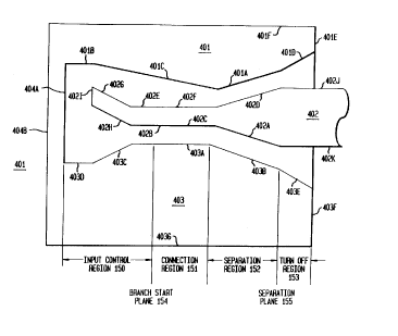
The electrode configuration 400 according to a preferred embodiment of the
present invention is described in detail in Figure 4. Figure 4 illustrates the
same regions,
input control region 150, connection region 151, separation region 152, and
turn off
region 153 as described previously in Figures lA and SA. In addition, Figure 4
illustrates
the branch start plane 154 and separation plane 155 as previously described in
Figures 1 A
and SA. The positioning of the electrode configuration 400 relative to the y-
shaped optical
switch 101 is shown in Figure 4. The electrode configuration 400 further
comprises three
electrodes 401, 402, and 403 as shown in Figure 4. Electrode 401 further
comprises edges
401A, 401B, 401C, 401D, 401E, and 401F. Electrode 402 further comprises edges
402A,
402B, 402C, 402D, 402E, 402F, 4026, 402H, 402I, 402J, and 402K. Electrode 403
further comprises edges 403A, 403B, 403C, 403D, 403E, 403F, and 4036. The
direction
symbols N, S, E, and W represent north, south, east, west and denote the
relative
positioning of elements in Figure 4.
Figure 4 is now explained in detail. Edge 402A begins at the separation plane
155,
preferably 3,um northeast of the upper edge 112 of the lower branch 108 of the
y-shaped
optical waveguide 101. It runs parallel to the upper edge 112 of the lower
branch 108 of
the y-shaped optical waveguide 101 and ends at the first intersection with the
lower edge
111 of the upper branch 107 of the y-shaped optical waveguide 101. Edge 402B
is
preferably 300~sm long. It begins at the branch start plane 154 and runs
preferably 300~m,
parallel to the upper edge 114 of the input 102 of y-shaped optical waveguide
101. It is
preferably 3/4 ~m south of the upper edge 114 of the input 102 of the y-shaped
optical
waveguide edge 100. Edge 403A begins preferably 3/4 ,um north of the lower
edge 115
of the input 102 of the y-shaped optical waveguide 101 and preferably 300~cm
to the west
of the branch start plane 154. It runs substantially parallel to the input 102
of the y-shaped
~~:1~ ~~r:Q
12
optical waveguide 101 until it intersects with edge 403B. Edge 403B begins at
the
separation plane 155, preferably 2,um southwest of the upper edge 112 of the
lower branch
108 of the y-shaped optical waveguide 101. It runs substantially parallel to
the upper edge
112 of the lower branch 108 of the y-shaped optical waveguide 101 until it
intersects edge
403A. Edge 402C connects edges 402B and 402A. Edges 401 A and 402D run
substantially parallel to the upper edge 110 of the upper branch 107 of the y-
shaped optical
waveguide 101. Edge 402D is preferably 2~m southeast of the upper edge 110 of
the
upper branch 107 of the y-shaped optical waveguide 101. Edge 401A is
preferably 3 ~cm
northwest of the upper edge 110 of the upper branch 107 of the y-shaped
optical
waveguide 100. Both edges begin at the separation plane 155 and run southwest,
stopping
along the same plane as the end of edge 402A. Edge 402E is substantially
parallel to and
preferably 5 ,um away from edge 402B. Edge 402F connects edges 402E and 402D.
Edges 4026 and 402H are substantially parallel and preferably 5 ~m apart. They
run to
the northwest, preferably 5 ~m north and 500 ,um west. Therefore edges 4026
and 402H
preferably have a northwest to the southeast slope of 0.01. A northwest to
southeast slope
is known as a negative slope in the relevant art. Edge 402I connects edges
4026 and
402H. Edge 403C runs southwest, preferably 5 ,um south and 500 ,um west.
Therefore,
edge 403C preferably has a northeast to the southwest slope of 0.01. A
southwest to
northeast slope is known as a positive slope in the relevant art. Thus, edges
402H and
403C have substantially equal and opposite slopes in the input control region
150, thereby
forming a smoothly (linearly, according to a preferred embodiment of the
present
invention) decreasing gap between them in the input control region 150. Edge
403D is
substantially parallel to the lower edge 115 of the input 102 of the y-shaped
optical
waveguide 101 and preferably 400 ,um long. Edge 401B is substantially parallel
to edge
403D and preferably 26 ~m north of edge 403D. Edge 401 C connects edge 401 A
to edge
401B. Edge 404A connects edge 401B to edge 403D. Edge 404B is substantially
parallel
to edge 404A and preferably 200 ,um west of edge 404A. It runs preferably 34
,um north
from and 28 ,um south from a center line 104 of the input of the y-shaped
optical
waveguide 101. Edge 401 D starts at the eastmost end of edge 401 A and runs
preferably
5 ,um north and 500 ,um east. Thus, edge 401D preferably has a southwest to
northeast,
13
i.e., positive, slope of 0.01. Edge 401E runs from the eastmost end of edge
401D to a
point preferably 34 ~cm from the center line 104 of the input of the y-shaped
optical
waveguide 101. Edge 401F connects edge 404B to edge 401E. Edges 402J and 402K
are substantially parallel to each other and the upper edge of the input 102
of the y-shaped
optical waveguide 101 and run east from the eastmost ends of edges 402D and
402A,
respectively. Edges 402J and 402K are used to connect the device to bond pads.
Edge
403E begins at the eastmost end of edge 403B and runs preferably 500 ~cm east
and 5 ,um
south. Thus, edge 403E preferably has a northwest to southeast, i.e.,
negative, slope of
0.01. Edge 403F begins at edge 403E and runs to a point preferably 28 ~cm
south of the
center line 104 of the y-shaped optical waveguide 101. Edge 4036 connects
edges 404B
and 403F.
Voltage differences between electrodes 401, 402, and 403 create an electric
field
between the electrodes 401, 402, and 403. The electric field thus generated is
illustrated
in Figure 3. Figure 3 is the same cross sectional view illustrated in Figure
6. In Figure 3
electric field lines 302, generated by voltage differences between the
electrodes, are
illustrated. The electric field lines 302 are directed perpendicular to the
electrode
configuration plane 303, and pass through the optical waveguide branches 107,
and 108.
The desired direction of the electric field is due to the crystalline
structure of the substrate
on which the electrodes 401, 402, and 403 are formed. In the preferred
embodiment, the
crystal is Z-cut lithium niobate (LiN03). Voltage applied to Z-cut LiN03
generates
electric field lines 302 down into the z-cut LiN03 crystal and through the
optical
waveguide 100 as shown in Figure 3.
The present invention provides smooth application of the applied voltage in
the
input control region 150. In the input control region 150 the applied field is
predominantly
controlled by the electrodes 402 and 403. This is because, as shown in Figure
SA, the y
shaped optical waveguide 101 is positioned generally between electrodes 402
and 403 in
the input control region 150. Thus, the electric field lines, as shown in
Figure 3, from the
voltage between electrodes 401 and 402 has little, if any, effect on the y-
shaped optical
waveguide 101 in the input control region 150. The applied electric field is
controlled by
decreasing the gap between the electrodes in a smooth manner. As described
above, the
v ' ,
14
strength of the applied field varies as V/L. Therefore, as the spacing between
electrodes
402 and 403, L, decreases, the electric field strength increases. The smoothly
(linearly,
according to a preferred embodiment of the present invention) decreasing gap
is bounded
by edges 402H and 403C in Figure 4. Thus, because the electric field strength
varies as
V/L, the electric field is increased smoothly, in the input control region
150. The electric
field is then maintained constant until the branch start plane 154 as shown by
the
substantially constant gap defined by edges 402B and 403A until the beginning
of the
branch start plane 154. Thus, light propagating in the waveguide experiences a
gradual
turn-on of the electric field through the input control region 150 of the y-
shaped
waveguide 101.
The electric field reaches an equal value in each branch 107 and 108 in the
separation region 152. In a preferred embodiment of the present invention, the
optical
switch 500 is manufactured from a birefringent material such as lithium
niobate (LiN03).
As a result, an electric field may be applied to the branches 107 and 108,
such that the
1 S electric field promotes light mode propagation in one of the branches 107
or 108 and
inhibits light mode propagation in the other of the branches 107 or 108. In
addition, the
branches 107 and 108 are coupled. Therefore, the power in the inhibited branch
107 or
108 is substantially fixlly transferred to the promoting branch 107 or 108.
Therefore, when
light reaches the end of the separation region 152, it will continue to
propagate through
only one of the branches 107 or 108.
A substantially constant electric field is applied to the branches 107 and 108
of the
y-shaped optical waveguide 101 in the separation region 152. Electrodes 401
and 402
maintain a substantially constant spacing in the separation region 152. This
substantially
constant spacing between electrodes 401 and 402 is illustrated in Figure 4 by
edges 401A
and 402D. Also, electrodes 402 and 403 maintain a constant spacing in the
separation
region 152. This substantially constant separation between electrodes 402 and
403 is
illustrated in Figure 4 by edges 402A and 403B. The spacing between electrodes
401 and
402 is substantially equal to the spacing between electrodes 402 and 403. The
substantially constant spacing between electrodes 401 and 402 and electrodes
402 and 403
generates a substantially constant electric field through the optical
waveguide branches 107
15
and 108 in the separation region 152. Optical outputs are taken at the end of
the
branches 107 and 108 of the y-shaped optical waveguide 101 at the separation
plane 155.
Maintaining a substantially constant electric field in the separation region
152, allows the
electrode design of the optical switch of the present invention to incorporate
the voltage-
s length reduction techniques, such as one described in W. K. Burns, "Shaping
the Digital
Switch," IEEE Photonics Technology Letters, Vol. 4., pp. 861-863, August
1992..
The electric field is turned off in a smooth manner after the light mode has
propagated beyond the separation plane 155 and into the turn off region 153.
Smooth turn
off of the electric field is accomplished by smoothly increasing the spacing,
L, between the
electrodes 401 and 402 and electrodes 402 and 403 in the turn off region 153.
The
smoothly (linearly, according to a preferred embodiment of the present
invention)
increasing spacing between electrodes 401 and 402 is illustrated in Figure 4
by edges 401D
and 402J. The smoothly (linearly, according to a preferred embodiment of the
present
invention) increasing spacing between electrodes 402 and 403 is illustrated in
Figure 4 by
edges 402K and 403E. The smooth turn off, like the smooth turn on, avoids
disturbing
the propagation of light in the waveguide.
Edge 402D is offset from the upper edge 110 of the upper branch 107 of the y-
shaped optical waveguide 100. Edge 403B is offset from the upper edge 112 of
the lower
branch 108 of the y-shaped optical waveguide 100. Offsetting the edges of the
electrodes
401, 402, and 403 optimizes the electro-optic effect of the applied electric
field. This
optimization is described in Marcuse, "Optimal Electrode Design for Integrated
Optics
Modulators," IEEE Journal of Quantum Electronics, Vol. QE-18, pp. 393-398,
March
1982.
The operation of the optical switch, designed according to the present
invention,
is now explained. Light enters the y-shaped optical waveguide 101 at its input
102. The
electrodes 401, 402, and 403 are designed to apply a smoothly (linearly,
according to a
preferred embodiment of the present invention) increasing electric field to
the y-shaped
optical waveguide 101. The electrodes 401, 402, and 403 smoothly increase the
electric
field. As will be appreciated by persons skilled in the relevant art, the
input control region
150 is the optimum point at which to begin application of the electric field.
The reason is
16
two-fold. First, crosstalk at the separation plane 155 is reduced. Second,
propagating
light is disturbed less if the electric field is turned on smoothly in the
input control region
150, rather than abruptly at a point further down the path of light
propagation.
Light propagating through the optical waveguide 101 enters the connection
region
151. The electrode design of the connection region 151 is primarily to connect
the
electrodes from the input control region 150 to the separation region 152.
Connection in
a smooth manner, as previously described, minimizes disturbing light
propagating through
the y-shaped optical waveguide 101 and minimizes crosstalk appearing at the
output of the
y-shaped optical waveguide 101 at the separation plane 155.
In the connection region 151, two nodes may appear due to the larger width in
the
y-shaped optical waveguide 101 where the y-shaped optical waveguide 101 begins
to
branch apart, i.e., the branch start plane 154. Because the y-shaped optical
waveguide 101
is a single mode optical waveguide, only a single mode of light will exist on
the branches
107 and 108 and in the input 102.
If no control voltage and, therefore, no electric field, is present across the
y-shaped
optical waveguide 101 branches 107 and 108, then equal amounts of light appear
at the
end of branches 107 and 108 of the y-shaped optical waveguide 100. The optical
output
of the digital optical switch can be taken at the separation plane 155. A
control voltage
(V) is applied to the branches 107 and 108 of the optical waveguide 100 to
generate an
electric field, which changes the index of refraction of the branches 107 and
108 of the
optical waveguide 101, by the electro-optic effect, The index of refraction is
changed such
that light mode propagation is promoted in one of the branches 107 or 108 and
inhibited
in the other branch 107 or 108 of the optical waveguide 100. In a preferred
embodiment,
the branches 107 and 108 are coupled. Therefore, the power of the light in the
inhibiting
branch is transferred to the promoting branch. As a result all of the power of
the input
light mode is switched into the promoting branch at the end of the separation
region 152.
As an example of a first application of voltage, suppose that a first voltage
(V/2)
is applied to electrodes 401 and 403. V can range from 1 to 100 volts. Assume
further,
that a second voltage (-V/2) is applied to electrode 402. In this case, light
propagating .
through the upper branch 107 of the y-shaped optical waveguide 101 is
promoted. A light
2~ ~~ ~ ~Q
17
mode propagating in the lower branch 108 of the optical waveguide 101 is
inhibited.
Furthermore, because branches 107 and 108 of the optical waveguide 101 are
coupled, the
power of the light mode in the inhibiting lower branch 108 of the optical
waveguide 101
is transferred to the promoting upper branch 107 of the optical waveguide 101.
According
to a second embodiment of the present invention, the polarities of the
voltages on the
electrodes 401, 402, and 403 are reversed, i.e., V/2 is applied to electrode
402 and -V/2
is applied to electrodes 401 and 403. In this case, upper branch 107 of the
optical
waveguide 101 inhibits light propagating through it. Lower branch 108 of the
optical
waveguide 101, on the other hand, promotes light propagating through it.
Furthermore,
because branches 107 and 108 of the optical waveguide 100 are coupled, the
power of the
light mode in the inhibiting upper branch 107 of the optical waveguide 101 is
transferred
to the promoting lower branch 108 of the optical waveguide 101. Therefore,
digital
switching, that is, routing of the input to one of two outputs, is
accomplished by the design
of the present invenrion.
The voltages applied to the electrodes of the present invention are not
constrained
to +/- V/2. According to a third embodiment, voltage is applied so as to hold
electrode
402 at ground or hold electrodes 401 and 403 at ground. The A value of +V or -
V is
applied to the electrodes not held to ground. In order to properly change the
index of
refraction, the voltage on the electrodes not held to ground reverses
polarity, i.e. swings
from +V to -V or from -V to +V. The change in voltage causes the index of
refraction of
the branches 107 and 108 to change such that digital switching, as described
above, is
achieved. Note, however, that the total voltage swing is twice V volts. Using
the first
embodiment, the voltage swing is only V volts. The V voltage swing of the
first
embodiment is preferable to the twice V voltage swing of the second embodiment
because
such a swing is accomplished faster and therefore can be used for higher data
rate
switching requirements.
While various embodiments of the present invention have been described above,
it should be understood that they have been presented by way of example only,
and not
limitation. Thus, the breadth and scope of the present invention should not be
limited by
any of the above-described exemplary embodiments, but should be defined only
in
2171120
1g
accordance with the following claims and their equivalents.