Note: Descriptions are shown in the official language in which they were submitted.
21 7 1 22~
ALIGNMENT OF PARITY BITS
TO P~IMINATE ERRORS IN 8h~ NG PROM AN
ACTIVP TO A STANDBY PROCESSING CIRC~IT
R~t~ of ~h~ Inv^ntl~n
This invention generally relates to a telecommnnication
network in which active and standby processing apparatus are
utilized in the processing and transmission of data. This invention
more specifically relates to the switching from the active to the
passive apparatus when the data being handled by the apparatus
includes hierarchical based parity bits.
It is common in a high reliability telecommunication network
to provide two substantially identical processing apparatus used in
processing and transmitting user data in the network. The pair of
apparatus is typically referred to as an active and standby
apparatus in which the active apparatus is engaged in processing and
transmitting user data with the standby apparatus being idle but
ready to assume responsibility for processing and transmitting the
user data. A change of processing from the active to the standby
apparatus enables the active apparatus to undergo maintenance and
testing to ensure its continued reliability or may occur due to a
failure of the active apparatus. It is, of course, desired that a
switch over or transition from the active to standby apparatus
handling the data transmission be accomplished with min;m~l, or
preferably, no disruption of user data processed by the apparatus.
Various types of error detection techniques are utilized to
detect errors in user data. The use of parity bits is well known in
the art. A parity bit or a group of bits are generated by a
calculation based on a collection of data to be protected. In a
binary system, an even parity bit or an odd parity bit is determined
based on whether the summation of a plurality of bits or bytes to be
protected result in a number that is even or odd.
Data is often transmitted in frames in a telecommnnication
network wherein the frame is constructed to contain a payload or
- 2 - 217l225
user data and a header which contains information utilized by the
network in processing the frame of data. Since such frames may be
constructed in a hierarchical manner to include and build upon
previously constructed subframes (partial frames), such hierarchical
constructed frames may result in the creation of hierarchical
generated parity bits in which a first parity bit protects a first
subframe, a second parity bit is based upon the first subframe plus
additional information, and additional subframes are similarly built
creating a hierarchy of subframes in which parity bits have a rank
based on the hierarchy. The higher parity bits are based on
subframe information and the parity bits of lower rank. Thus, the
upper rank parity bits protect not only the data, but the integrity
of the lower ranked parity bits.
While this technique provides increased reliability in
detecting errors in the frame, such hierarchical parity bits present
problems when the apparatus utilized to generate such a frame is
desired to be switched from an active to a standby apparatus. This
problem arises because the standby apparatus will normally not have
been processing the previously generated frames of information at
the time of the desired switch from the active to the standby
apparatus. "Nested~' parity bits are based on one or more prior
frames in order to insure error protection over a series of such
frames. The standby apparatus will not, upon the time of switch
over from the active device, be capable of immediately generating
2s the correct nested parity bits for the next frame to be transmitted.
This occurs because the standby apparatus has not processed the
prior frames of data which i6 required in order to determine the
correct nested parity bits to be embedded in the first frame to be
transmitted by the standby apparatus.
One approach to this problem is to disregard the history of
the previously generated nested parity bits by the active apparatus
and to begin transmission with a frame generated by the standby
apparatus with a new series of parity bits. However, at least the
first frame generated by the standby apparatus using this technique
will result in parity bits which will appear to indicate erroneous
- 3 - 21 71225
associated data to the receiving equipment in the network (or end
user equipment) which decodes the parity bits. Thus, this technique
may result in the receiving equipment rejecting several frames of
data as being erroneous. A request for the retransmission of such
data may be made based on the perceived incorrect parity. In some
system designs such a changeover operation may be acceptable.
However, in systems where the requirement for the retransmission of
a plurality of frames of data may represent unacceptable delays in
the reception of correct data at the receiving equipment or in
systems in which erroneous data may elicit undesirable maintenance
activity, this technique may not prove acceptable. Thus, there
exists a need for an improved technique for ~-king the transition
from an active to a standby apparatus in a telecommunication network
where nested hierarchical parity bits are employed.
~mm--Y f ~L~U~L-~L9~
It is an object of the present invention to provide a so ution
to the above need and provide an inventive step in the art by
providing for glitchless switching from active to standby apparatus
in which hierarchical nested parity bits are generated. As used
herein, ~glitchless~ switching refers to the ability to make an
active-to-standby eguipment changeover with no incorrect parity bits
being transmitted.
In accordance with an embodiment of the present invention, a
method is provided for permitting glitchless switching between
active and standby telecommlm-cation apparatus which generates
hierarchical nested parity bits. In accordance with the
illustrative embodiment, a third order hierarchical parity bit
technique is accommodated by synchronizing frames to be transmitted
by the standby apparatus to the proper parity bit conditions prior
to the transfer from the active apparatus to the standby apparatus.
In the exemplary embodiment, first, second, and third parity bits
are utilized wherein the third parity bit protects a third subframe
of data, a second parity bit protects a second subframe of data
which includes the third subframe of data including the third parity
bit, and the first (highest rank) parity bit resides in a first
- 4 - 21712~5
subframe and is also based on both the third and second subframes
and hence, is based on both the third and second parity bits as well
as the other included information.
Beginning with a first frame, the standby apparatus starts
generating subframes and the nested parity bits. However, until the
parity bits associated with the frames generated by the standby
apparatus are aligned with the corresponding parity bits in frames
generated by the active apparatus, the output frames transmitted to
the network continue to be frames generated by the active apparatus.
In the exemplary embodiment, three parity bits must be aligned to
have the same polarity or state as the correspon~;n~ parity bits
generated by the ongoing active apparatus. In accordance with the
exemplary embo~i - t of the present invention, the decision of
whether to invert each parity bit is sequentially made by order of
the rank of the parity bit. For example, the lowest ranked parity
bit (deepest embedded parity bit) is determined first, the next
lowest parity bit determined next, and the highest order parity bit
(rank N) determined last.
In accordance with an important recognition made in accordance
with the present invention, it has been discovered that the previous
inversion of a lower ranked parity bit will influence different
parity alignment decisions. Thus, the history of lower ranked
parity bit inversions is needed. Predetermined parity bit inversion
sequences are stored for each of the possible decision branches
which may be followed based on whether the corresponding ranked
parity bits associated with the active and standby sides are equal
and on whether a lower ranked parity bit has been previously
inverted.
In accordance with the illustrative embodiment of the present
invention, the standby apparatus aligns each of the three ranks of
parity bits in a frame so that each equals the corresponding parity
bit in the active side. Thus, after such processing, a transition
can be made from the active to standby apparatus without incurring
any perceived errors in data due to incorrect parity bits by
2171225
equipment receiving the frames of data. This provides a glitchless
switching capability.
~rlef n~rtDt~n of ~h^ nr~w~s
FIG. 1 illustrates a block diagram of an exemplary apparatus
S which generates frames of data which includes nested hierarchical
parity bits.
FIGs. 2, 3, and 4 illustrate a first, second, and final frame
formats, respectively, for information processed by the apparatus as
shown in FIG. 1.
FIG. S illustrates a block diagram of an embodiment in
accordance with the present invention in which frames including
hierarchical parity bits are generated by active and standby
processors.
FIG. 6 is a block diagram of an ~mho~ nt of the interface
circuit as shown in FIG. 5.
FIG. 7 is a flow diagram of a method in accordance with an
embodiment of the present invention illustrating steps utilized to
align the hierarchical nested parity bits.
D~ r~Dt~n
FIG. 1 illustrates an exemplary multilevel processor 10 which
generates frames of data including user information to be
transmitted through a telecommunication network. The processor 10
includes a plurality of frame a~sembly stages which each add
additional data and utilize parity bits calculated in a hierarchical
nested technique to provide error protection. An information
payload as~embler 12 receives and assembles user data from either a
single or a plurality of sources for transmission through the
teleco~nnication network. A grouping of such user data is
assembled in a known manner to form a payload on a frame-by-frame
basis. The user data is combined as indicated by addition node 14
with additional information generated by path processing circuit 16.
The path processing information includes information such as status,
user identification, a parity bit, and other information which may
be considered collectively as a first header. This information is
combined with the assembled user data from assembler 12 by node 14.
- 6 - 21712~5
`
The output of node 14 (header 1 and payload 22) is read by a bit
interleaved parity processor 18 which generates the lowest ranked
parity bit (B3) in the exemplary embodiment. This parity bit is
transmitted to the data processing circuit 16 for inclusion with the
next generated frame of data generated by node 14. Each frame
(actually a subframe) generated by node 14 carries a parity bit
which was determined based upon the data~contained in the preceding
frame (subframe).
Referring to FIG. 2, the data format of the subframe 20
lo generated as an output from node 14 includes a payload 22 consisting
of the assembled user data by assembler 12, and h~d~r 24 generated
by path processing circuit 16. In the exemplary embodiment, a bit
interleaved parity byte 26 comprises part of header 24 and is
generated by parity generator 18. In the illustrative embodiment,
an 8-bit parity byte 26 is included in which each of the eight bits
corresponds to the parity of the correspo~;ng bits carried by 8-bit
bytes of payload 22 and header 24. For example, the first bit of
the 8-bit parity byte 26 consists of a bit defining an even or odd
parity based on the addition of the corresponding first bits of all
the other bytes associated with a subframe 20. Each of the
successive bits 2-8 of the parity byte corresponds to an even and
odd parity for the correspon~lng bits 2-8 of all the other bytes
carried in the subframe 20. It will be apparent to those skilled in
the art that the specific parity protection may vary, based on the
grouping of bits and bytes to be protected by corresponding parity
bits and bytes.
Returning to FIG. 1, a line processing circuit 28 provides
additional information including a second priority byte to form what
may be considered as second header which is attached to subframe 20
by addition node 30. A second bit in~erleaved parity byte (B2) is
generated by parity generator 32 and inserted by the line processing
circuit 28 during the generation of each frame (subframe).
FIG. 3 illustrates the data format of a subframe 34 as output
from node 30. As will be apparent, this subframe includes all the
information contained by subframe 20 and further includes additional
- 7 - 21 71 225
._
information contained in a second header 36 including a second 8-bit
parity byte 38. The parity byte 38 is constructed similarly to that
previously explained with regard to parity byte 26 in that each of
the 8 bits comprises even and odd error protection of the
correspon~;ng bits in the bytes contained in subframe 34. However,
parity byte 38 also provides error protection of the previously
generated parity byte 26 and thus, parity byte 38 will vary in
accordance with changes in the preceding parity byte 26 as well as
changes of other data bytes in subframe 34. Also, as explained with
regard to parity byte 26, the parity byte 38 included in one
subframe is calculated based upon the data contained in the
preceding subframe 34 transmitted from node 30. It will be apparent
to those skilled in the art that the illustrative parity bytes will
be received and stored by the end receiving equipment wherein the
appropriate parity bytes will be applied to the data of the previous
frame in order to permit an error detection calculation to be made
by known parity calculation techniques.
Returning to FIG. 1, the subframe 34 is combined with
additional information which may be considered as a third header
generated by section processing circuitry 40 which is added to
subframe 34 by node 48. The information included in the third
header includes a final (highest order) parity byte (B1) generated
by bit interleaved parity generating circuit 44. The frame has
additional information generated by section processing circuitry
which forms part of the third header. A final resulting frame 54 is
transmitted on transmission ch~nnel 50 and is routed to
telecommunication network 52. In accordance with the exemplary
embodiment, the generation of sequential frames of data is provided
by the multilevel processor 10.
FIG. 4 illustrates the data format of the final (complete)
frame 54 to be transmitted on channel 50. Frame 54 includes
subframe 34 together with a third header 56 which includes a first
(highest) rank parity byte 58. Like the previously explained
generation of the lower ranked parity bits, the generation of parity
byte 58 is based on the previously generated frame and includes
- 8 - 2 1 7 1 2 2 ~
error protection of all information contained in the last frame 54
including the parity bytes 26 and 38. A change of a bit in parity
byte 26 will "ripple~ or propagate to change parity bytes 38 and 58.
Likewise, a change to a bit in parity byte 38 will cause changes to
parity byte 58, but, of course, would not impact the lower ranked
parity byte 26. Thus, for the standby apparatus to generate frames
with correct parity bits, i.e. equal to the parity bits generated by
an active apparatus, frame boundaries and the history of the prior
parity must be known. The parity bytes generated by the new standby
frame must be aligned to reflect the corresp~n~ng data history,
i.e. avoid the transmission of parity bits which appear to indicate
errors in the data to the receiving equipment even though the
received data has no errors. An exemplary embodiment of apparatus
and an exemplary method in accordance with the present invention
which are described below address this transition problem.
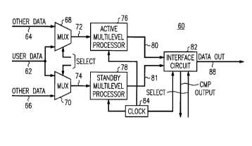
FIG. 5 illustrates a block diagram of a telecommunication
apparatus 60 in accordance with an emho~i t of the present
invention which generates sequential frames of data protected by
nested hierarchical parity bits. User data i8 received on
co~mication chAnnel 62. Other types of data may be received as
inputs on communication chAnn~ls 64 and 66. Selectors
~multiplexers) 68 and 70 select one of two inputs to feed via
communication chAnnels 72 and 74 to the active multilevel processor
76 and the standby multilevel processor 78, respectively. In the
illustrative embodiment it will be understood that the labels
"active~ and "standbyn refer to a given time of operation and that
the roles of the multilevel processors can alternate between active
and standby. The active label normally designates the multilevel
processor which is actively receiving user data, processing the data
and transmitting the user data on an output chAnnel to interface
circuit 82. The interface circuit receives clock inputs from clock
84 as does the active and standby processors. Interface circuit 82
selects whether to transmit output frames generated by the active or
standby processors on output channel 88 to receiving equipment
connected to output chAnnel 88.
~ 9 ~ 2171225
-
Each of the processors 76 and 78 may comprise an apparatus
such as shown in FIG. 1 which generates or builds frames based on
input data. Assume active multilevel processor 76 is receiving user
data from chAnne1 62 via selector 68 and rhAnnel 72, while standby
multilevel processor 78 receives other data from rhAnnel 66 by
selector 70 and input chAnnel 74. In this condition the processor
76 generates frames carrying the user data which are transmitted to
interface circuit 82 which then couples the frames to output 88 for
transmission to appropriate receiving apparatus. While this
activity proceeds, standby multilevel processor 78 may receive test
or maintenance data which is utilized to exercise or test the
functions of the processor 78. Processor 78 generates output frames
based on the test data and transmits these frames on output rhAnnel
81 to interface circuit 82. Interface circuit 82, which will be
described in more detail below, selects between one of its inputs to
process. In the illustrative example, input 80 is selected to be
processed by interface circuit 82 and a resulting output transmitted
on rhAnnel 88. Input on rhAnnel 81 representing the testing of
processor 78 is not transmitted by the interface circuit to chAnnel
88, but can be routed to other circuitry associated with such
testing (not shown).
Assuming that processor 78 is operating in the standby mode
and that it is desired to reverse the modes of the processors, that
is, have processor 78 assume the active role while processor 76
assumes the standby role, user data 62 will be selected by both
selectors 68 and 70 to provide concurrent inputs on rhAnnels 72 and
74 to both processor 76 and 78, respectively, prior to the desired
time of transition. In accordance with a preferred, but not
exclusive mode of operation of an embodiment of the present
invention, user data is routed to the standby processor 78 for a
sufficient number of frames before the actual switch over is made to
transmit data generated by standby processor 78. In the
illustrative example, at least one frame of user data will have been
forwarded to and processed by the standby processor 78 prior to the
desired frame at which the transition is to occur. This gives the
2171225
-- 10 --
interface circuit 82 time to implement the steps in accordance with
the present invention to achieve parity bit alignment so that
"correct" parity bits are always transmitted on chAnnel 88. That
is, there will be glitchless switching with agreement between data
and parity bits for all frames transmitted by interface circuit 82
regardless of the switch from active to passive processing from
processor 76 to processor 78.
FIG. 6 illustrates a block diagram of an interface circuit 82
in accordance with an embodiment of the present invention.
Registers 90 and 92 are associated with the active and standby
processors 76 and 78, respectively, and receive frames generated
from the processors on input chAnnels 80 and 81. Prior to a
transition to be made from the currently active processor 76 to the
passive processor 78, a first frame of data is generated by both of
the processors and transmitted to interface circuit 82 on lines 80
and 81, respectively. Inversion circuits 94 and 96 process these
frames stored in registers 90 and 92, respectively. The inversion
circuits are used to selectively invert or change the polarity
(state) of the lowest rank parity bit 26; the remainder of the frame
is unchanged. A comparison circuit 98 compares parity bit 26 of the
standby frame with the correspon~;ng parity bit 26 of the
correspon~ing active frame and provides control signals on output
lines 100 to the inversion circuits. Co~p~rison circuit 98 sends an
output signal on line 100 to inversion circuit 96 to control whether
parity bit 26 is to be inverted based upon whether it is equal to
the corresp~n~;ng parity bit in the active side of the same frame.
Once this decision has been made, the comparison circuit 98 also
transmits the comparison decision by path 101 to comparison circuit
106. In all succeeding frames the inversion circuit 96 will either
invert or not invert the parity bit 26 based on the decision made
during the current frame by comparison circuit 98. However, once
parity bit alignment is attained, the same decision for following
frames will continue to be made unless an actual parity error
exists. Inversion circuit 94 may have been inverting or not
inverting the active side parity bit 26 prior to the first frame
-11- 2171225
the inversion choice of circuit 94 (the active side) remains
unchanged during the active-to-standby changeover.
The explanation in accordance with FIG. 6 and the following
explanation of the method steps in accordance with FIG. 7 describe a
transition and comparisons with regard to a single parity bit as
opposed to the parity byte as discussed with regard to FIGs. 1-4.
It will be understood that with regard to each bit in the parity
byte the same correspo~i ng decisions will be made on a bit-by-bit
basis since each parity bit is calculated indep n~ent of the other
parity bits.
Inversion circuits 102 and 104 receive the frames as processed
by inversion circuits 94 and 96, respectively, and store
predetermined parity inversion patterns (sequences) which are
selected. The inversion circuits 102 and 104 invert or do not
invert parity bit 38 deppnAing upon the results of the comparison
made by comparison circuit 106 and the prior inversion decision made
by comparison circuit 98. The co~rArison circuit 106 determines
whether the parity bit of the second rank (parity bit 38) of the
standby frame is equal to the corresps~ing parity bit 38 in the
corresponding active frame. The decisions by circuits 106 and 98
are transmitted on path 107 to comparison circuit 114. The output
signals on control lines 108 from comparison circuit 106 are used to
control inversion circuits 102 and 104. In the illustrative
example, the inversion circuit 104 will receive and implement the
inversion or non-inversion sequence as determined by the signal on
line 108 from comparison circuit 106 during the current frame. This
permits the state of the lower rank parity bit 26 previously
determined by comparison circuit 98 and implemented by inversion
circuit 96 to be used as part of the inversion determination of each
bit in parity byte 38. The state of inversion or non-inversion of
bits of the byte 38 by the active side circuit 102 is not changed.
circuits 102 and 104 do not change data in the processed frame
except for the parity bits in the byte 38.
Inversion circuits 110 and 112 receive the frames from
circuits 102 and 104, respectively, and store predetermined
` - 12 - 2171225
sequences of inversions which are applied during the changeover from
the active to standby apparatus. The inversion decision implemented
by circuit 112 depends on whether comparison circuit 114 determines
if the corresp~n~ing standby parity bit 58 is equal to the
corresponding parity bit 5B in the active side during the same frame
and on prior inversion decisions made by circuits 98 and 106. In
accordance with the illustrative embodiment, this determination is
implemented by control signals on output lines 116 from comparison
circuit. This decision i8 made for each frame, but as explained
above, will not vary once parity bit alignment is achieved. The
state of inversion or non-inversion of active side bit 58 by circuit
110 is not changed.
The frame output from inversion circuits 110 and 112 are
received as inputs by shift registers 118 and 120 which each store a
frame of data. The frame output on lines 122 and 124 from registers
118 and 120, respectively, provide inputs to comparator 126 which
provides a bit-by-bit comparison of these frames. The true/false
result of the complete frame comparison is provided on output line
128 and provides a means by which a determination is made that the
standby side frame is in parity synchronization (alignment) with the
active side frame, i.e`. all parity bits in the standby side frame
are equal to correspon~ing parity bits in the active side frame
prior to making the transition. The frame output on lines 122 and
124 from the registers is also provided as inputs to selector 130
which selects either the active or standby frame of data to be
coupled to the data output line 88 from interface circuit 82. A
select control signal carried on line 132 determines which of the
frames are selected. A system controller (not shown) receives the
true/false signal from line 128 and is utilized to provide a control
signal on select line 132 which prevents a transition from the
active to the passive data stream until a true signal is received on
line 128.
Assuming a transition is desired from the active to the
passive processor, and assuming that the active processor has not
encountered an actual failure, a frame of data is processed by the
- 13 - 2171225
-
standby processor 78 in parallel with the active processor 76 in
order to enable the comparison circuits 98, 106, and 114 to make
decisions as to whether the corresponding standby inversion circuits
96, 104, and 112 are to implement an appropriate inversion sequence
5 of the parity bits 26, 38, and 58, respectively. Thus, in
- accordance with a preferred embodiment of the present invention, at
least one frame is processed prior to the actual transition of
transmitting frames processed by the standby processor 78. It will
be apparent to those skilled in the art that once a transition has
been made from the active processor 76 to passive processor 78, the
roles are reversed and the side then selected to provide output
frames of information becomes the active side, i.e. processor 76 is
then the standby side and processor 78 is the active eide. A
6ubsequent active to standby transition causes the decisions made by
comparison circuits 98, 106, 114 to result in correspo~ing
inversion decisions to be implemented by the then standby inversion
circuits 94, 102, and 110, respectively, while the decisions
implemented by circuits 96, 104, and 112 remain lmch~nged.
FIG. 7 illustrates a flow diagram in accordance with an
exemplary emho~iment of the present invention which illustrates
steps which may be implemented by the apparatus shown in FIG. 6.
Beg; nni n~ at START 150, a determination is made by step 152 of
whether the lowest ranked parity bit in the standby side is equal to
the correspo~ing parity bit in the active side, i.e. is B3A=B3s?
2s Where ~Bn represents a parity bit, ~3~' indicates rank, and the
subscripts specify A(ctive) or S(tandby) association. As previously
explained, the B3 parity bit inversion is first determined. A N0
determination by step 152 resultæ in the lowest ranked parity bit on
the standby side (B3s) being inverted as indicated in step 154. The
decision to invert or not invert the lowest parity bit is made
during each frame. In accordance with the exemplary embodiment, the
notations B3, B2, and B1 correspond to the lowest, intermediate, and
highest ranked parity bits 26, 38, and 58, as shown in FIGs. 2, 3,
and 4. It will also be appreciated that the steps described for
- 14 - 21 7 1225
-
Fig. 7 are made on a bit by bit basis for each corresponding parity
bit of the three parity bytes.
Regarding the correction of B2, a YES decision by
determination step 152 leads to a further determination by
5 determination step 156. The determination made by step 156 is
whether the parity bit 38 in the standby side is equal to the
corresponding parity bit 38 for the same frame in the active side,
that is, is B2A.B2s? A NO determination by step 156 results in step
158 causing an inversion decision for the parity bit 38 (B2S). This
lo decision is stored and implemented, i.e. B2s is to be inverted. A
YES determination by step 156 results in a decision not to invert
the second ranked parity bit.
With regard to the correction of B2, if the determination made
by step 152 was NO, then an inversion determination for the second
ranked parity bit proceeds as follows. Contin~ g from the
inversion of B3s in step 154, a determination is made in step 160 to
apply an inversion sequence to the second order parity bit, wherein
the sequence consists of inverting the second ranked parity bit
during frames of even n-~mher. That is, during frame numbers 2, 4,
6, ...., the second ranked parity bit 38 (B2s(N) ) is inverted; it is
not inverted during odd numbered frames. Following step 160, a
determination is made in 6tep 162 of whether the 6econd ranked
parity bit following the inversion provided in step 160 is equal to
the correspon~ing parity bit in the active side, i.e. is B2A=B2s? A
NO determination by 6tep 162 results in step 164 implementing an
inversion to be made of each second parity bit B2s.
With regard to the correction of Bl, it will be apparent from
FIG. 7 that inversion decisions for the highest ranking or first
parity bit 58 (Bls) will be made depen~i ng on which of the four
decision paths from the correction of B2 is taken. If step 164 was
executed, then the highest parity bit will be inverted in accordance
with the sequence determined in step 166 where Bls is inverted for
frame numbers 3, 4, 7, 8, 11, 12, .... That is, inversions will be
made in pairs of two with non-inversion being made in intermediate
- 15 - 217l~5
pairs of two. This indefinite sequence is continued in accordance
with step 166.
In the correction of B1, a YES determination by step will
result in the highest rank frame B1s being inverted in accordance
s with a frame sequence of 2, 3, 6, 7, 10, 11,.... , as indicated in
step 168. If step 158 was executed, the highest ranked parity bit
Bls will be inverted in accordance with even numbered frames as
indicated in step 170. That is, the highest order parity bit Bls
will be inverted during frames 2, 4, 6,....
If the determination step 156 resulted in a YES determination,
no preceding inversions of the third or second parity bits will have
been initiated. This, as well as steps 166, 168, and 170, leads to
a detenmination in step 172 to make a determination as to whether
the highest parity bit in the standby side is equal to the
correspon~;ng highest parity bit during the current frame in the
active side, i.e. does BlAsB1s? A NO determination by step 17
results in the highest order parity bit Bls being inverted in
accordance with step 174. A YES determination by step 172 results
in the termination of the alignment process at END 176. The
inversion decisions made for B3s, B2s, and B1s are made seguentially
and implemented for all frames until the next active-to-standby
transition.
In accordance with the illustrative embodiment of FIGs. 1-4 in
which 8-bit parity bytes were used, the above actions of FIG. 7 are
taken for each of the eight parity bits in each parity byte since
each parity bit provides an independent indication of parity for
corresp~n~ing bit positions in the other data as previously
discussed. Thus, for an 8-bit parity byte, the above inversion-
determ;ning process will be independently made for each of the 8
bits in the parity bytes.
As described in FIG. 7, steps 160, 166, 168, and 170 involve
the implementation of a predetermined bit inversion sequence based
on the frame number (position) relative to a first beginning frame
It is believed to be apparent to those skilled in the art that such
repeating sequences can be implemented in various ways including
- 16 - 2171225
`
state machines, logic circuits, and software processes. In
accordance with the preferred embodiment of the present invention,
in order to enhance the processing speed, it is preferred that
inversion decisions and bit inversions be implemented in hardware.
It is believed to be apparent to those skilled in the art that this
exemplary technigue explained with regard to three levels of
priority can be utilized to handle various levels of nested parity
bits including parity ranks of 2, 3, and greater than 3.
Inver~ion 8-gu-nc-
~
In the above description in accordance with FIGs. 6 and 7,
predetermined inversion sequences of the parity bits are utilized
depPn~ing upon the comparisons of the standby-to-active parity bits
and dep~n~i ng upon the prior history of inversion decisions made
with regard to lower ranked parity bits. This section provides an
explanation of why the particular inversion patterns defined in
steps 160, 166, 168, and 170 are used to achieve parity bit
alignment.
These relationships compare the parity calculated by the
active and standby apparatus. For these calculations, frame 1
corresponds to the first frame in which the active and standby
apparatus are processing equivalent data. The parity inserted in
frame 1 by the active and standby sides may be different since the
two sides were processing different data prior to frame 1.
In the following expressions the value in parentheses
indicates the frame in which the correspon~l ng data or parity bits
occur. B3(N+1) is the B3 parity bit 26 inserted in frame N+1, where
D3(N) includes all of the corresponding payload 22 and header 24
data bits in subframe 20 of frame N in FIG. 2, except the B3 parity
bit, which may be different between the active and standby sides and
is shown separately as B3(N). B2(N+1) is the B2 parity bit 38
inserted in frame N+l, where D2(N) includes all of the corresponding
payload 22 and header data bits 24 and 26 in subframe 34 of frame N
in FIG. 2, except the B3 and B2 parity bits 26 and 38, which may be
different between the active and standby sides and are shown
separately as B3(N) and B2(N), respectively. Similarly, Bl(N+1) is
- 17 - 2111225
-
the B1 parity bit 58 inserted in frame N+l, where D1 (N) includes all
of the correspon~ing payload 22 and header data bits 24, 36, and 56
in subframe 54 of frame N in FIG. 2, except the B3, B2, and B1
parity bits 26, 38, and 58, which may be different between the
active and standby sides and are shown separately as B3 (N), B2 (N),
and B1(N), respectively.
B3(N+1) = D3(N)+B3(N)
B2(N+1) = D2(N)+B3(N) +B2(N)
Bl (N+1) = D1(N)+83(N)+B2(N)+B1 (N)
In the following expressions, parity and data correspon~jng to
the active and standby sides are designated by the subscripts A and
s, respectively (e.g. B3A,B3S).
The following relationships compare the B3 parity calculated
and inserted by the active and standby apparatus.
ACTIV~ SInF B3A(N+l) = D3(N)+B3A(N)
SPAR~ ST~ B3s(N+l) = D3 (N)+B3s(N)
Note that the header and payload data represented by D3 (N) is
equivalent for the active and standby sides. Thus:
B3A (N+1) -B3s(N+l) = B3A(N) -B3s(N)
The above equation can be further re~Yce~ by iteratively
substituting for B3 in previous frames.
B3(N-1) = D3(N-2)+B3(N-2)
B3(N) = D3 (N-l)+B3 (N-l)
B3(N+1) = D3(N)+B3(N)
B3 (N+l) = D3 (N) +D3 (N-l) +D3(N-2)+...+D3(1)+B3(1)
- 18 - 21 7 1 ~25
B3A(~+1)-B3S(N+~ ,D3(n)+ B3A(1)
~, D3~n) + B3S(I)
_n-l
B3A(N + 1) - B35(N + 1) = B3A(1) - B3s(l)
The above calculation shows that the difference in the B3
parity for the active and standby sides is determined by the
relationship between the correspon~ing B3 values in the first frame,
i.e. B3A(1) and B3s(l). There are two conditions which can occur,
lS either B3A(1)~B3S(1) or B3A(1)-B35(1).
FOR B3A(1) = B3S(1): B3A(N + 1) - B35(N + 1) = O
B3A(N +l)= B3S(N +l)
FOR B3A(1) ~ B35(1) B3A(N + 1) - B3S(N + 1) = 1
B3A(N+l)= B3s(N+l)
Thus, for B3A(1)-B3S, the B3s and B3A parity bits will be equal
in all 6ubsequent frames. For B3A~ B35(1), B3s will be the
inverse Of B3A in all subsequent frames. B3s can be made equal to
B3A by comparing their values in correspnn~;ng frames and if not
equal introducing an inversion in the parity for the standby side as
shown in FIG. 7.
The following relationships compare the B2 parity calculated
and inserted by the active and standby apparatus.
ACTIVE SIDE B2A(N + I ) = D2(N) + B3A(N) + B2A(N)
SPARE SIDE: B2S(N + 1) = D2(N) + B3S(N) + B2S(N)
-19- 2171225
-
Iteratively substituting for B3 and B2 in previous frames:
B2(N -1) = D2(N - 2)+ B3(N - 2) + B2(N - 2)
B2(N) = D2(N -1) + B3(N -1) + B2(N -1)
B2(N + 1) = D2(N) + B3(N) + B2(N)
B2(N + 1) = [D2(N) + D2(N ,1)+...+D2(1)]
+[B3(N) + B3(N - 1)+. ..+B3(1)]+ B2(1)
N
B2A(N + 1) - B2S(N + 1) = ~ B3A(n) + B2A(1)
_ n-l _
N
- ~ B3s(n) + B2S(1)
_n-l
To solve for B2 in EQ 1, the cases must be considered for
which B3A=B3s and B3A~ B35.
FOR B3A = B3S: B2,,(N + 1) - B2s(N + 1) = B2A(1) - B2S(1)
FOR B2A(1) = B2s(l): B2A(N + 1) = B2s(N + 1)
FOR B2A(1) ~ B2s(l ): B2A(N + 1) = B2S(N + 1)
Thus, for B3A(1)=B3S(1), the relationship between B2s and B2A is
dependent on the relationship between B2A(1) and B2s(l). For
B2A(1)~B2S(1), the B2s(1) and B2A parity bits will be equal in all
subsequent frames. For B2A(1) ~ B2S(1), B2S will be the inverse of B2A
in all subsequent frames.
FOR B3A ~ B3S:
N N
FORN EVEN ~--B3A(N)_~B35(N)=
n~l n=l
N N
FOR N ODD ~ B3A(N)- ~ B35(N) = 1
n=l n=l
Substituting the above relationships into EQ 1:
- 20 - 2l 11225
`
FORN EVEN: B2A(N+l)-B2s(N+I)=B2A(l)-B2s(l)
Note that the above relationship is the same as for the case
S when B3AZB3s. Thus, for B3A.'B3S and N even, B2S will either equal
B2A or be the inverse, depe~ing on whether B2A(1)~B2S(1) or
B2A(1)~B2S(1), respectively.
10FOR N ODD B2A(N + 1) B2S(N + 1) = B2A(1) _ B25(1) + 1
= B2A(1)- B2S(1)
15FOR B2A(1) = B2s(1): B2A(N + 1) = B2s(N + 1)
FOR B2A(1) ~ B2s(1): B2A(N + 1) = B2s(N + 1)
The above relationship shows that for B3A~ B3s and N odd, B2s
will either be the inverse of B2A or equal to B2A, depending on
whether B2A(1).B2S(1) or B2A(1)~B2S(1), respectively. This
relationship taken together with the previous relationship for N
even shows that the relationship between B2s and B2A for B3A~B3S is
the opposite for odd and even frames. This difference can be
accounted for by inverting B2s in every other frame as shown in FIG.
7, after which B2s will either equal B2A or its inverse in every
frame.
The following relationships compare the B1 parity calculated
and inserted by the active and standby apparatus.
BI A(N + 1) = D1(N) + B3"(N) + B2A(N) + B1"(N)
Bls(N + 1) = Dl(N) + B3s(N) + B2S(N) + Bls(N)
Iteratively substituting for B3, B2, and B1 in previous frames:
B1(N-I)= D1(N-2)+B3(N-2)+B2(N-2)+B1(N-2)
40Bl(N) = Dl(N -1) + B3(N -1) + B2(N -1) + B1(N -1)
Bl(N + I ) = D1(N) + B3(N) + B2(N) + B1(N)
- 21 - 217l225
N N
Bl(N + 1) = Dl(n) + ~ B3(n)
n-l n-l
h'
+2~, B2(n) + Bl(l )
n-l
n-l n-l
B2(n) = ~, D2(m) + B3(m) + B2(1)
~-1 m-l
N N n-l n-l
~, B2(n) = ~ , D2(m) + 2~, B3(m) + B2(1))
n-l n-l m.l ~n-l
N N n-l N n-l
2~: B2(n) = ~ D2(m) + 2~: ~ B3(m) + (B2(1) x N)
n-l n-l m-l n-l ~-1
N N
2 o BIA(N + I ) = ~, Dl(n) + ~ B3A(n)
n-l n-l
N n-l H n-l
+~, 2~ D2(m) + ~, ~, B3A(m) + (B2A(I ) x N) +BI A(I )
n-l ~.1 n.l ~.1
N N
Bls(N + I) = Dl(n)+ ~B3S(n)
n-l n-l
N n-l N n-l
+~D2(m)+~B3s(m)+(B2s(l)x N)+BIS(I)
n-l m=l n-l /n~
-22- 2l71,2~25
N N n-l ~
BIA(N+I)-BIS(N+~ B3A(n)+ '.~ B3A(m)+(B2A(I) x N)+ Bl~(l)
_n.l n~
N N n-l
~ 2~;B3S(n)+ ~,B3s(m)+(B2s(l) x N)+ B1S(I)
_n.l n.l ~.1
BlA(N + I) - BlS~N + 1~ [B3A(n) ~ B3S(n)]+
n.l
BO 2
~ ~ [B3A(m) ~ B3S(m~j~ +(B2A(I)- B2S(I))X N + B1A(1)- B1S(1)
n.l
To solve for B1, the following cases must be considered:
Case 1: B3A=B3S and B2AB2S;
Case 2: B3A~B3S and B2A~B2S;
Case 3: B3A$B3S and B2A=B2S;
Case 4: 83A$B3S and B2A~B2S-
FOR B3A = B3s
B1A(N + 1)- B1S(N + 1) = (B2A(1)- B2S(1))X N + B1A(1)- B1S(1)
r~ qR 1
25 FOR B2A = B2S
BlA(N + 1) - Bls(N + 1) = B1A(1) - BlS(I)
Thus, If B1A~1)=B1S then B1A(N + 1) = B1S(N + I )
If B1A(1)~B1S~1) then B1A(N+1)= Bls(N+I)
Thus, for Case 1:
If B1A~1).B1S(1), the Bls and B1A parity bits will be
equal in all subsequent frames. If B1A~ B1S~1), Bls will be the
inverse of B1A in all subsequent frames.
- 23 - 2 1 7 1 225
~QR 2:
FOR B2,,, ~ B2S:
For N even: If B1A(1).B15(1) then Bl~(N+I)=Bls(N+I)
If B1A(1)~B1S(1) then Bl ~(N + I )= Bls(N + 1)
FOR N ODD Bl A(N + 1) - Bl s(N + 1) = 1 + EnA(l) - BlS(l)
If B1A ( 1 ) Bls ( 1 ) then B1"(N + 1) = Bls(N + 1)
If B1A(1) ~Bls(l) then Bl~(N+l)=Bls(N+l)
Thus, for caBe 2:
For N even, if B1A(1).B15(1), the BlS ~nd B1A parity bits
will be equal in subsequent frames. If B1A(1)~B1S(1), BlS will be
the inverse of B1A in subsequent frames.
For N odd, if B1A(1)-B15(1), B1S will be the inverse of
B1A in subseguent frames. If B1A(1)~B1S(1), the Bls and B1A parity
bits will be equal in subsequent frames.
FOR B3" ~ B3s
~[B3A(n)- B3s(n)]= 0 for N EVEN
"- t
~Q~
~, [B3~,(n) - B3s(n)]= 1 for N ODD
H r,-l N ~I-t
~ ~ [B3,t(m) _ B3s(m)]' = ~1
~1 , n-l ~/~t
N ~,_ I N
[B3~(m)-_ B3S(m)]' = ~ (n -1)
~-1 .1 , 11-1
- 24 - 2171225
-
~ ~ [B3~(m)~ B3S(m)]' = 2 = 0 for N = 1,4,5,8,9,12,13, . . .
n~
N '~
S ~ [B3A(m)--B3S(m)]' = 2 = 1 for N = 2,3,6,7,10,11,
n- l ~
Substituting the values for B3 given in Eqs 3 and 4 into EQ 2:
10Bl ~(N + 1) - Bls(N + 1) = [B2A(1) - B2s(1)]X N
+B1A(1)- BIS(I); for N = 3,4,7,8,...
15= [B2A(1)- B2s(l)]x N
+BIA(1)- BlS(l)+l; for N = 1~2,5,6,. . .
r. ~ 3:
FOR B2A = B2S
BIA(N + 1) - ~s(N + 1) = B1A(1) - BlS(l); for N = 3,4,7,8,. ..
= BlA(l)_ Bls(l); for N = 1~2,5,6,....
B1A(1) = B15(1) B1A(N + 1) = B15(N + 1); N = 3,4,7,8,.
BIA(N + 1) = BlS(N + 1) ; N = 1,2,5,6,. . .
B1A(1) ~ B1S(1): BlA(N + 1) = Bls(N + l); N = 3,4,7,8,. -
BIA(N +I)= Bls(N +l); N = 1,2,5,6,. . .
Thus, for Ca~e 3:
35For B1A(1).B1S(1), BlS will be equal to B1A in frames
4, 5, 8,9,...and the inverse of B1A in frames 2,3,6,7...
For B1A(1) ~BlS(l), Bls will be the inverse of B1A in frames
4,5,0,9,...and equal to B1A in frames 2,3,6,7,...
2171225
-- 25 --
-
~CR 4:
FOR B2A ~ B25:
FOR N E VEN: [B2A(I)- B2s(l)]X N = 0
B1A(N +1)- B1S(N +1)= B1A(1) - BlS(l); for N = 4,8,12,...
= B1A(1)- B1S(1); for N = 2,6,10,...
FOR N O DL~.[B2A(I)_ B2S(1)]X N =1
B1A(N +1)- B1S(N +1)= B1A(1)- B1S(1); for N = 3,7,11,
= B1A(1)- BlS(l); for N = l,S,9,...
2o B1A(1) = Bls(l): BlA(N + 1) = Bls(N + 1); N = 1,4,5,8,9,
B1A(N +1)= B1S(N +1); N = 2,3,6,7,10,11,.
B1A(1) ~ B1S(1) B1A(N +1)= B1S(N +1); N = 1,4,5,8,9,
B1A(N +1)= B1S(N +1); N = 2,3,6,7,10,11,. . .
Thus, for Case 4:
For B1A~1)=B15(1), B1s will be equal to B1A in frames
2,5,6,9,10,...and the inverse of B1A in frames 3,4,7,8,11,12...
For B1A(1) ~B1s(l), B1s will be the inverse of B1A in frames
2,5,6,9,10,... and equal to 81A in frames 3,4,7,8,11,12,
The differences between B1S and B1A as determined for Cases 1-4
can be accounted for by introducing the appropriate inversions in
Bls as shown in FIG. 7.
Although an embodiment of the present invention has been shown
in the drawings and described in the above description, the scope of
the invention is defined by the claims which follow.