Note: Descriptions are shown in the official language in which they were submitted.
r~ r ~
~ WO 95/10870 2 1 7 1 3 3 7 PCT/GB94/02239
OPTICAL PUIISE SEO~ ; GENERATOR
BACKGROUND TO THE INVENTION
The present invention relates to a method and
apparatus for generating a desired optical pulse sequence
in response to an input optical signal. The invention also
encompasses an all-optical switch based on such pulse
generation techniques. The present applicants~ earlier
International application PCT/GB93/00863 filed 26th April
~0 1993, and the paper by K. Smith and J.K. Lucek, Electronic
Letters,28,1814 (1992) disclose a system in which a pulse
sequence input to a modulator in the cavity of a mode-
locked laser results in the laser outputting a clock signal
corresponding to the timing waveform of the input data,
i.e. having an output pulse corresponding to each bit
position of the input pulse sequence, irrespective of
whether there is a one or a zero (a pulse or a null) in a
given bit position.
This clock may be used in producing a regenerated
signal but this requires a further stage in which the
recovered clock is modulated by the original signal.
SUMMARY OF THE INV~:NllON
According to a first aspect of the present invention,
there is provided a method of generating an optical pulse
sequence comprising applying a repetitive optical signal to
an optical modulator connected in the laser cavity of a
mode-locked laser, and outputting a pulse sequence from the
laser cavity, characterised in that the repeat period of
the repetitive optical signal is equal to, or an integer
multiple of, the cavity round-trip time, the laser thereby
being driven to output pulses in bit positions
corresponding to the non-zero pulses of the input
repetitive optical signal.
The first aspect of the present invention provides an
all-optical method for generating a desired pulse sequence.
The output pulse sequence is found to have superior pulse
SUBSTI~TESH~(RULE~
2t71337
WO9S/10870 PCT/GB94/02239 ~
characteristics with reduced noise and timing jitter, and
so is suitable to be used as a regenerated signal to
replace the input signal. As further described below, the
output pulse sequence may also be used, for example, in the
operation of an all-optical demultiplexer, or in other
signal processing or switching devices.
The present inventors have found that if a repetitive
signal, such as a repeated multi-bit word, or a sequence of
OTDM frames all having zeros in certain predetermined bit
positions, is used as the input data stream for a modulator
in a laser cavity, and if the repetition period is matched
to the round trip time of the cavity, or a multiple
thereof, then instead of outputting a clock signal, the
laser replicates the input pulse sequence. That is, the
output from the laser, although as before being locked to
the timing of the input pulse sequence, now has zeros where
there are zeros in the input pulse pattern, or, in the case
of an OTDM frame, zeros in those bit positions
corresponding to those channels in the programming data
stream which are set OFF .
Preferably the laser is arranged to continue to output
the pulse sequence after the input pulse sequence has been
removed or modified.
The method of this aspect of the invention may be used
to provide an optical memory which maintains the pulse
sequence at its output even after the original generating
sequence has been removed. To this end, the cavity may
include a pulse shaping element so that it functions as a
hybrid active/passive mode-locked device. Then, after
initial active mode-locking in response to the input pulse
stream, the laser remains passively mode-locked to sustain
the output pulse sequence. Appropriate pulse shaping
devices are discussed in the above-cited paper and
International application. Alternatively, the laser may be
actively mode-locked by an additional modulator driven by
an appropriate clocking signal.
SUBSTITUTE SH~FT (RU~E 2~;)
:`- 2~7~337
~ WOg~/10870 pcTlGBs4lo2239
According to a second aspect of the present invention,
there is provided a method of controlling an optical
switch,
characterised by a applying a repetitive optical
signal to a modulator connected in the cavity of a laser
thereby mode-locking the laser, the repeat period o~ the
repetitive optical signal being equal to or an integer
multiple of the cavity round-trip time,
outputting the pulse train generated in the cavity in
response to the applied repetitive optical signal, and
applying the pulse train or a signal derived therefrom
to the control input of an optical switch arranged to route
incoming data to different outputs depending on the state
of the signal at the control input.
15This aspect of the invention provides a method of
programming an optical switch such as an OTDM (optical time
division multiplexing) demultiplexer which can be
implemented using solely optical programming signals
thereby avoiding the limitations in switching or control
speeds which arise where electronic programming is used.
The repetitive optical signal may be a signal generated
locally for the specific purpose of programming the
demultiplexer, or may be the OTDM signal itself. In this
case the programming can be controlled remotely by
appropriate switching of the OTDM signals at the signal
source or sources followed by transmission of the signals
over a network to a switching node. When the programming
signal is an OTDM signal, then it is the zeros in the bit
positions corresponding to the non-selected channels which
are repeated. The other bit positions carry data pulses
and so may vary from repetition to repetition, provided
that on average the value of each of these bit positions is
non-zero.
Preferably signals from one of the different outputs
of the optical switch are applied to the modulator in the
optical cavity to provide the said repetitive optical
signal. Preferably the method includes setting the optical
S~BSTITUTE SH~Er (RU~E 2f;)
2 ~ 7 I 3 3 7
WO95/10870 pcTlGBs~lo2239 ~
switch to a state in at least part of each input pulse is
output at the said one output, irrespective of the state of
the control input, and in which the data stream at the
input is non-zero only in those bit positions corresponding
to the OTDM channels which are to be selected by the
demultiplexer.
In the preferred implementation of this aspect of the
invention, the output of the optical switch, comprising
signals in those bit-positions selected in response to the
control signal at the control input of the switch, is
applied to the modulator in the cavity of the mode-locked
laser. This then drives the mode-locked laser to output
further control pulses in those selected bit-positions
which are in turn applied to the control input of the
switch, and so on. The whole system then operates in a
self-sustaining loop.
Before the self-sustaining steady-state condition
described above is set-up, the system is initialised by a
start-up procedure. In this procedure, initially only the
channels to be selected are turned on in the data stream
supplied to the data input of the switch. But since there
is not yet an appropriate control sequence at the input to
the switch, the switch is, for the duration of this phase,
set in a state such that all the input data is transmitted
to the output connected to the mode-locked laser. For
example, in the preferred implementation using a loop
mirror, this is done by biasing the loop to be partially in
reflecting mode and partially in transmitting mode in the
linear regime. The data transmitted through the switch
then drives the modulator in the laser to produce the
required control pattern at its output. Once that control
output is set-up the switch can be returned to its normal
operating condition in which data is only switched to the
output connected to the laser when there is a coincident
control pulse at the control input. The method may include
inputting a first OTDM data stream and one or more
additional data channels to the switch and substituting the
SIJBSTITUTE SH~ET (RULE 2~;)
WO95/10870 i - 2 1 7 1 3 3 7 PCT/GB94/02239
.
additional data channel or channels in the data stream
output from the switch.
The switch may be used to carry out more complex
functions than simply dropping channels from an OTDM data
stream. In particular it can be used to add in channels
from a second source. This function can be extended to
provide full cross-switching of two or more input OTDM data
streams. In the case of a switch formed as a NOLM, this
may be done using circulators at the input and output of
the loop. Appropriate switching structures are described
in further detail below.
According to a third aspect of the present invention,
there is provided an optical switching system comprising
an optical switch having at least one signal input and
a plurality of signal outputs and a control input, and
an optical pulse sequence generator comprising a mode-
locked laser having a modulator connected in the laser
cavity and including an input for a repetitive optical
signal which in use is applied to the modulator, the cavity
having a round-trip time such that the repeat period of the
repetitive optical signal is equal to or an integer
multiple of the said round-trip time,
the output of the optical pulse sequence generator
being connected directly or indirectly to the control input
2S of the optical switch and the switch thereby routing
incoming data to different outputs depending on the state
of the signal at the control input.
BRIEF DESCRIPTION OF THE DRAWINGS
Embodiments of the different aspects of the present
invention will now be described, by way of example only,
with reference to the accompanying drawings in which:
Figure 1 is a diagram illustrating a first example of
a pulse generator circuit;
Figures 2a and 2b are schematics illustrating the
operation of the circuit of Figure 1;
~UBYITUTESH~ (RULE~
2 1 7 1 3 3 7 PCT/GBg4102239
WO9S/10870
Figures 3a to 3f are intensity/time plots illustrating
experimental data obtained using circuits embodying the
present invention;
Figure 4a is a circuit diagram showing a remotely
programmable OTDM network node, and Figures 4b and 4c are
schematics of a cascaded pair of nodes and a node
respectively;
Figure 5 is a diagram showing schematically an
alternative embodiment of a pulse generator circuit;
Figure 6 is a diagram showing schematically a further
alternative embodiment;
Figure 7 is a diagram showing a modified non-linear
loop mirror for use in the circuit of Figure 4a;
Figures 8a and 8b are diagrams illustrating the use of
the loop mirror of Figure 7;
Figure 9 is a schematic of an optical network having
a bus topology;
Figure 10 is a schematic of a switch
Figure 11 is a word-forming network for use in the
circuit of Figure 10;
Figures 12a and 12b are schematics of alternative
embodiments of a switch and;
Figure 13 is a further example of an OTDM switch.
DESCRIPTION OF EXAMPLES
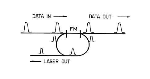
Figure 1 shows a first example of a circuit
implementing the present invention. A fibre laser 1 is
configured in a loop and incorporates a fibre modulator 2
in the optical cavity. A transmission fibre 3 is also
connected in common with the fibre modulator.
In this example, the fibre laser is based on an
erbium-doped fibre (operating range 1.52 - 1.66 nm) pumped
by a high power laser diode LD which may be a GRINSCH
InGaAsP device.
The modulator comprises a single-mode optical fibre
which, in the present example, has a length of 8.8km. A
suitable fibre is available commercially under the trade
SUBSTITUTE SHEET (RU~E 26)
=
WO 95tlO87~ 2 1 7 1 3 3 7 PCT/GB94/02239
.
name SMF/DS CPC3 from Corning Inc., a US corporation of
Corning, New York 14831. This is a dispersion-shifted
fibre designed to operate in the 1550nm region. It has a
mode field diameter of 8.1 microns, a cladding diameter of
125 microns and a coating outside diameter of 250 microns.
The effecti~e group index of refraction is 1.476 at 1550nm.
. ~ In the circuit of Figure 1, each of the couplers WDM1,
WDM2 is a bi-directional device incorporating an
interference filter formed as an evaporation-deposited
stacked dielectric. One wavelength passes straight through
the filter while another wavelength is reflected. An
appropriate device having these properties is available
commercially from the company JDS FITEL as WDM coupler
model no.WD1515Y-A1. A similarly constructed wavelength-
selective coupler WDM3 is used to couple a laser diode pump
to the fibre laser.
The circuit further comprises an optical filter F
which may be an interference filter, used to control the
frequency and width of the pulse in the laser cavity. An
intra-cavity fibre isolator I ensures that the cavity
function unidirectionally. A suitable isolator is model
no. OIC-1100-1550 from BT & D Technologies. The output
from the cavity is coupled by a fused fibre coupler, such
as model no. SMC0202-155-OC from BT & D.
In use, a pulse sequence carried on the transmission
fibre is input to the fibre modulator where it cross-phase
modulates light propagating in the laser cavity, thereby
mode-locking the laser. In systems embodying the present
invention, mode-locking is carried out using one of the
higher harmonics of the cavity, rather than the fundamental
mode. The laser cavity therefore contains a number of
independent pulse trains. In the example shown
schematically in Figures 2a and 2b, three data bits arrive
at the modulator for every round-trip of the laser and each
one of the three bits drives one of the three laser pulses
in the ring.
Sl IBSTI~UTE SHEET (RULE 26)
2 ~ 7 1 337
WO95/10870 PCTIGB94/02239
In the present examples, a repeated synchronized word
is supplied to the modulator on the transmission fibre
(Figure 2b). The arrangement is as in Figure 2a, the only
difference being that now the laser is presented with a
repetitive three bit sequence ("ll0" in this example).
Each bit in the three bit sequence modulates a particular
pulse in the ring laser. If the data bit is a "l" then a
laser pulse is generated. If the data bit is a "0" then
the laser is not modulated and no laser pulse arises in
that time-slot. The output of the laser is therefore
modulated with the same data sequence as the input data
stream. In general, a laser driven at the mth harmonic of
the mode-spacing can be mode-locked to a word that is m
bits long, or to a word that is an integer divisor of m
bits long.
In the example of Figure l, the erbium fibre ring
laser is mode-locked at around l.007GHz by a stream of
- 20ps pulses drived from a gain-switched DFB laser. The
continuous stream applied to the fibre modulator on the
transmission fibre was encoded using a LiNbO3 amplitude
modulator and a data generator. Since L, the
characteristic length of the cavity, is approximately equal
to 9km, giving c/nL of 23kHz, the driving frequency
corresponds approximately t o the 44000th harmonic of the
mode-spacing, i.e. n~44000 so that there are 44000 pulses
in the ring cavity at any one time. For the first example
shown in Figure 3a, the driving data stream is set to a
repetitive eight bit sequence "ll0l00l0". The repetition
rate is tuned to a mode of the ring cavity in order to
force laser mode-locking. By stepping the frequency up or
down in c/nL increments or decrements a pulse can be added
or subtracted from the ring cavity. At a particular ring
mode corresponding to 8n pulses in the cavity, where n is
an integer, the laser generates at its output the same
"ll0l00l0" repetitive sequence. As described previously,
the laser output is in the form of a low jitter stream of
SUBSTITUTE SHEET (RUI E 26)
WO9S/10870 2 ~ 7 1 3 3 7 PCT/GB94/02239
near transform-limited pulses with a duration of around
1 Ops .
Figure 3c shows the output of the laser when the data
repetition rate is stepped one mode-spacing up or down such
that there are 8n+1 or 8n-1 laser pulses respectively in
the ring cavity. This means that after each round-trip a
laser pulse has slipped one bit with respect to the eight
bit word in the driving data stream. Therefore, after
eight round-trips, each laser pulse has been modulated by
all the bits in the word. In this case, the resulting
laser output consists of a continuous stream of l's. This
mode of operation is then essentially equivalent to that
described in our above cited international application. If
alternatively the slip is set so that each laser pulse does
not see all of the modulating data bits, then the laser
output takes the form of a word where some of the bits are
either "1" or "0" depending on how many l's that bit was
modulated by on average, depending also on the exact laser
parameters and the data word.
The pulse generator may also be used to carry out
logic operations on the driving word. Figures 3(d) to 3(f)
show outputs obtained when the bit-rate is 8n+4 times the
cavity frequency. Counting from left to right in the
figures, the first and fifth bits see a ..111111.. pattern
of driving pulses; the second, third, sixth and seventh
bits see a ..101010.. pattern and the fourth and eighth
bits see a ..000000.. pattern. By altering the conditions
within the laser cavity, we can alter the generated
pattern. In (e) and to a greater extent in (f) pulses that
see a .. 111111... pattern are favoured over those that see
the a .. 101010... pattern. Thus if we regard the driving
word as a pair of four bit words, in (d) we see the result
of an OR operation between corresponding bits in the two
words and (f) we see the result of an AND operation.
The component indicated with dashed lines in Figure 1
is an optical pulse shaping element which may optionally be
included in the laser cavity. The inclusion of such an
STITUTE SH~ET (RULE 2~i)
WO 95/10870 r ~ 2 t 7 1 3 3 7 PCT/GBg~/02239
element changes the cavity from being entirely actively
mode-locked to being partially or entirely passively mode-
locked, that is a train of pulses once set up in the cavity
becomes self-sustaining. The inclusion of such a pulse
shaping element makes the circuit effective as an optical
memory. That is, the programming data stream input to the
modulator may be removed whilst still maintaining at the
output of the laser cavity a pulse stream reproducing the
pattern of the programming data. Such an optical memory
has applications in a number of fields including optical
processing or logic circuits.
The pulse shaping element may be provided by a further
fibre modulator chosen to be soliton supporting at the
optical powers at which the circuit operates, or
alternatively, may be formed, for example from a non-linear
semiconductor wave guide. In either case, the function of
the element is to sharpen the pulses in the cavity,
countering the tendency of the pulses to broaden in the
absence of a modulating signal in the fibre modulator.
Figure 4 shows a remotely optically programmable OTDM
(optical time-division multiplexing) network node based on
an optical sequence generator in accordance with the
invention.
The steady-state operation of the device is as
follows. The data enters a non-linear loop mirror (NOLM)
at A. Control pulses from a pulse generating circuit PG as
described above enter the loop through port E. If a
control pulse is present at the loop mirror at the same
time as a given data bit, then that bit is transmitted
through the loop and emerges at B. Otherwise, that data
bit is reflected and emerges at C. That is, the loop is in
the reflecting mode in the linear regime. The control
pulse pattern, e.g. 11001000, is repeatedly output from the
pulse generator PG in response to the repeated driving
signal and thus only bits in the first, second and fifth
channels are ever transmitted through the loop. This
demultiplexed data passes through the fibre laser and
SUBSTITUTE SHEET (RULE 2~)
~ 2 1 7 1 3 3 7 PCT/GBs4/02239
Wo95/10870
.
11
emerges at F. Delays within the circuit are controlled so
that the control word output from the pulse generator PG is
bit-synchronized with the input data at the loop mirror.
Then the first bit of the control pattern is coincident
with the first channel of the data stream and so on.
Prior to the steady-state condition described above
being established, the node goes through a start-up
procedure. Initially the loop mirror is biased to be
partially in reflecting mode and partially in transmitting
mode in the linear regime. This is done using a
polarisation controller within the loop to alter the
polarisation state of the light. Initially, only the
channels to be demultiplexed are turned on at the input to
the node. Each data pulse is partially transmitted through
the loop. Thus the pattern generator receives, in the
present example, a repeated ddOOdOOO pattern where d is a
data pulse which may be 1 or 0, and over several
repetitions has a non-zero time-average. A pattern of the
form 11001000 is generated at the output of the pulse
generator and is fed back to the control pulse input of the
loop. The non-linear phase shift imparted by the control
pulses on the data in the loop increases the proportion of
each pulse transmitted through the loop. The loop bias is
then changed so that it is completely in reflecting mode in
the linear regime. The data pulses are still transmitted
however as they are coincident with the control pulses,
hence the pattern generator still continues to produce the
11001.000 control pulse pattern. Now if the other channels
are switched on then since the loop is in reflecting mode
in the linear regime, and no control pulses are coincident
with the data in these other channels, those ch~nnels are
reflected from the loop. As shown schematically in Figure
4c, a number of such programmable network nodes may be
chained together. In use, the nodes can all be programmed
remotely in a cascade: that is the first (upstream) node is
programmed in the manner described above, and the channels
SU~STiTUTESH~ (RULE ~
r ~ 2 1 7 1 3 3 7
WO9S/10870 - PCT/GB9~/02239
12
not selected at that node are then used to program the next
node downstream, and so-on.
As an alternative to changing the loop mirror from a
partially transmitting state to a fully reflecting state
after the completion of the start-up phase, the loop-mirror
may be left permanently in a state in which it is, say, l~
transmitting in the linear regime. This means that a
portion of each channel that is switched on after the
start-up reaches the ring laser, however these channels do
not create pulses within the laser because the power
required to create pulses in the laser cavity is greater
when pulses already exist than when there are no pulses in
the cavity. The disadvantage of this arrangement is that
the extinction ratio is compromised: the demultiplexed data
streams contain a small amount of light in the empty
chAnnels .
Although the above examples are described using fibre
technology, the present invention is by no means limited in
this respect and other types of optical components and
circuits may be used. For example, the embodiment of
Figure 5 shows a pattern generator based on a hybrid
semiconductor/fibre circuit. The first element in the
circuit is a semiconductor gain medium and a saturable
absorber integrated with the gain medium and arranged to be
pumped by the incoming repetitive optical signal. The
output of the semiconductor is coupled to an external fibre
cavity incorporating a fibre grating end reflector.
Figure 6 shows a further alternative embodiment using
purely semiconductor components. In this case, the laser
cavity is defined between the end walls of the
semiconductor component. Again the semiconductor
incorporates a saturable absorber aligned with a gain
medium in a ch~nn~l formed in a semiconductor substrate.
A Bragg filter may be incorporated in the structure to tune
the device to a required wavelength.
Figure 7 shows a modified form of the loop mirror L
for use in the circuit of Figure 4a. In this modified
SUBSTITUTE SH~ET (RU~E 2~)
WOgS/10870 = 2 1 7 1 3 3 7 PCT/G~94/02239
13
loop, optical circulators Cl, C2 are provided on the input
and output branches of coupler 2. Appropriate circulators
are manufactured by Optics for Research as model number OC-
IR2-3 and available commercially in this country from
Lambda Photometrics Limited of Harpenden, Hertfordshire.
Such circulators in general use a crystal of the type known
as a Faraday rotator. This has the property that the plane
of polarisation of incident light is rotated in the sa~e
direction irrespective of the direction of travel through
the crystal. The crystal is arranged with polarisers on
its input and output such that the circulator functions as
a three port device. Light entering the device at port 1
emerges from port 2, light entering at 2 emerges from 3,
and light entering at port 3 emerges from 1.
Using the circulators, it becomes possible to add
channels at the node, as well as dropping channels. The
optical control pulses applied to the loop determine the
port from which a given data bit emerges. In the example
shown schematically in Figure 8a the loop is used to drop
or demultiplex one channel from an OTDM pipe and add
another channel in its place. The data stream to be added
is introduced at port PD in such a way that the pulses
within that channel arrive at the same time as pulses
within the channel to be dropped. A data pulse at port PD
will emerge from port PB and hence is merged with the non-
dropped part of the OTDM data stream. Such a function has
been carried out, for example, in a system in which a
10Gbit/s channel was dropped from a 40Gbit/s data stream
and another channel added in its place. This function can
be extended to a full cross-connect function (Figure 8b),
in which fully populated OTDM data streams arrive at both
ports PA and PD. In this case, the presence of a control
pulse results in the exchange of a bit between the two data
streams. An array of such devices can be used in an OTDM
node, allowing data channels from several incoming pipes to
be switched onto outgoing pipes.
SUBSTITUTE SHF~ (RULE~
WO95/10870 ~ 2 1 7 1 3 3 7 PCT/GBg~/02239
14
As an alternative to the use of a fibre modulator to
provide the non-linearity for the loop, other devices may
be used. For example, a semiconductor amplifier may be
used as the non-linear material. Also, high numerical
aperture (NA) optical fibres may be used.
The network of nodes described above with respect to
Figure 4b can be extended to include an ADD function as
described above. Tributary data streams may be included
in the added channels. The nodes are started-up in a
sequence which proceeds from the first upstream node to the
following downstream nodes.
Figure 9 shows a network having a bus-type topology.
In the Figure circles denote remotely programmable nodes as
described above, and squares denote data sources or
terminations. In the sequence described below, once a data
channel has been switched on, it is left switched on. The
appropriate start up sequence for such a bus network is
then as follows:
switch on chAnnels at D to be dropped at C, start
up node C
switch on channels at A to be dropped at B, start
up node B
switch on channels at A, D, E to be dropped at G,
start up node G
switch on channels to be sent from F and
r~mA; n ing chAnnels at A, D and E - these all
arrive at H.
Figure 10 shows a further example of an OTDM switching
node embodying the present invention. In this example the
pattern generator is used in a clock recovery and division
stage, and its output, rather than being applied directly
to control the switch, is processed by a gating pattern
generator.
The demultiplexer of this example comprises an optical
routing switch 101, providing a cross-connection between
two optical inputs lA, lD, and two optical outputs lB, lC.
The switch has a further input lG for gating pulses which
SUBSTITUTE SHET (RULE 26)
7 ~ 3 3 7
WO9~/10870 PCT/GB94/02239
.
determine the setting of the switch. In the absence of a
pulse at the input lG then an optical pulse input at lA is
fed straight-through to lB. In the presence of a pulse at
input lG a pulse input at lA, is cross-connected to output
lC.
The appropriate control sequence for the input G is
generated by splitting one of the input optical data
streams using, for example, a 50:50 fibre coupler. The
signal is then applied to a clock recovery and division
circuit 102 which generates a clock signal at, e.g., 1/n of
the bit-rate of the n-channel OTDM frames. The resulting
optical clock pulse train is passed through a gating pulse
pattern generator 103 to provide the pulse sequence which
is applied to the control input G.
The clock recovery division circuit in this example is
provided by a fibre-loop mirror demultiplexer as described
above with reference to Figure 4a. This device is started
up in the usual way with only one of the n channels being
transmitted during the start-up sequence. As a result the
output from the device is locked to the clock of the input
data stream but has a repetition rate of 1/n of the
original line rate.
The gating pattern generator is shown in more detail
in Figure 11. It contains a splitter/delay line/combiner
arrangement 105. The different paths provide different
respective delays for the split input optical pulse. The
delays are such that each input pulse results in n output
pulses, the pulse spacing being equal to the OTDM bit
spacing. Each arm of the network contains a shutter 106
that passes or blocks light. Thus the pattern of clock
pulses required to gate the routing switch can be generated
by controlling the status of each shutter. The shutters do
not have to have an ultra-fast switching time so they can
be electrically controlled and linked, for example, to a
remote control centre responsible for configuring the
network paths. A simple implementation of the device may
use commercially available fibre couplers and solenoid-
.
SUBSTITUTE SH~ET (RU~E ~6)
,
2 1 7 1 3 3 7 PCT/GBg~/02239
WO95/10870
16
controlled moving-fibre switches. An appropriate switch is
model no. SWllS manufactured by JDS Inc. of Canada and
commercially available in the U.K. from AG Electro-optics
of Tarporley, Cheshire. This switch functions by
mechanically inserting an element into the path of an
optical beam. Alternatively and preferably the gating
network may be an integrated device using planar silica
waveguide technology. The shutters in such an integrated
network may be semiconductor laser amplifiers SLAs. The
SLAs when turned ON can be used to provide gain, as well as
carrying out the shutter function. Appropriate planar
silica technology is disclosed in the paper by Cassidy et
al, BT Technology Journal, Volume ll, Page 1377 (1993). As
a further alternative, the optical pathways and splitters
can be formed from passive semiconductor waveguides with
active overlays to define SLAs to act as shutters.
Figure 12a shows an alternative embodiment in which
instead of a single routing switch, a 2x2 array of cross-
connect routing switches is used. This example allows four
input OTDM pipes to be connected to four output pipes. The
example shown is a blocking array. That is to say not all
combinations of cross-connections are possible. For
example, a channel from A cannot be routed to E at the same
time that B is routed to F. A non-blocking array could be
constructed although this would require additional cross-
connect routing switches. For example, the corresponding
non-blocking array shown in Figure 12b, known as a Benes
array, requires six cross-connect routing switches. In
either case, only one shared clock recovery device is
required. If each cross-connect switch is to have a gating
pattern independent of the others, then one gating-pulse
pattern-generator is required per switch. In the example
shown in the Figure, there are four input pipes and four
output pipes, each carrying six time-multiplexed channels.
The diagram shows where each input channel ends up e.g.
"A3" means channel 3 from pipe A. Each switch is driven by
SUBSTITUTE SHEET (RULE 2~;)
r
WO95/1~870 2 ~ 7 1 3 3 7 PCT/~B94/02239
.
17
a repeated six-bit pattern of control pulses. In the
example shown the control pulse patterns are:
w 001110
x 000101
y 110100
z 010110
where the irst bit of each sequence coincides with
the arrival of bits from channel 1 at the corresponding
switch, and so on. The figure shows the state of the array
when the channel 3s are being switched. It will be
understood that it is not a true "snap-shot" at one instant
of time, since in reality the control pulses at x and z for
a given channel should arrive later than the control pulses
at w and y for that channel to take account of the time for
the data to propagate between switches. The data path-
lengths between w and x, w and z, y and z, y and x must be
equal.
Figure 13 shows a further example of an OTDM switching
node which, as in the example described immediately above,
uses a gating pattern generator. In this example, the data
being processed has in each frame a he~er bit which is
always set to zero. Then when such frames are applied to
a first optically mode-locked laser 131 as described above
with reference to Figure 1, the resulting pattern generated
by the laser provides a frame synchronisation signal. The
use of the present applicant's optical pattern generator to
produce a frame synchronisation signal in this manner is
proposed in the paper by M. Obro, P. Thorsen and S.B.
Andreasen published at PP 1243-1244 Electronics Letters
21st July 1994, volume 30, number 15.
Having generated in this manner a frame
synchronisation pattern of the form .. 111110, the pattern
is inverted. This is done by using the pattern to control
a delayed version of itself input to a first optical gate
132 via a delay (e.g. a fibre loop of appropriate length)
135. The delay is set to be any integer number of bit
periods such that the zeros within the pattern and the
SUBSTITUTE Slt~ET (RULE 2~)
WO95/10870 2 1 7 1 3 3 7 PCT/GBg4102239
18
delayed version of the pattern are not aligned in time at
the gate 132. Then a bit arriving at the signal input of
the gate 132 is routed to output port 1 only from the one
bit position in which there is a zero at the control input.
For all other bit positions, where there is a 1 at the
control input, the signal is output to port 2. The output
from port 1 is then an inverted form of the fra~me
synchronisation signal and this signal is fed to a gating
pattern generator 133 which functions in the manner
described with respect to the embodiment of Figure 10.
This results in an appropriate gating pattern which is
applied to a second optical gate 134, again in the fashion
described above.
The optical gates 132 and 134 may both be formed from
non-linear loop mirrors in which the two pulse trains
involved are distinguished by having orthogonal
polarisations. In the case of the gate 132, the two pulse
streams involved are at the same wavelength, by contrast
with the previous examples in which signals were
distinguished by different wavelengths, and the different
polarisation states are therefore needed to separate the
different pulse streams.
In the example shown, in order to separate the first,
second and fourth channels from the remaining channels, the
pattern of gating pulses produced by the pattern generator
133 is 110100.
SUBSTITUTE SH~T (RULE 2~)