Note: Descriptions are shown in the official language in which they were submitted.
2171375
MANUFACT~KING ~ OF A SILICON WAFER HAVING A CONT~QT.T.~n
BMD CON~.~ATION IN THE BULK AND A GOOD DZ LAY~K
BACRGROUND OF TH~ lNV ~:N'l'lON
1. Field of the Invention
The present invention relates to a silicon wafer for a
semiconductor device and its manufacturing method. The
invention also relates to a high-quality silicon wafer for such
a semiconductor device as a VLSI.
2. DescriPtion of the Related Art
Silicon wafers are cut out of a single crystal silicon
ingot. A silicon single crystal can be manufactured ~y the
-10 Czochralski method, in which material polysilicon is placed in
a crucible of quarts glass (SiO2), and while it is melted ~y
heating, a silicon single crystal is pulled up and grown ~y
using a seed crystal.
In general, oxygen is dissolved in a silicon single
crystal produced ~y the Czochralski method. This is due to a
phenomenon that oxygen is dissolved into a molten silicon
liquid from the quartz cruci~le. In a cooling process after
the pulling of a single crystal, it is caused to have a
temperature history (cooling history) from the solidifying
temperature (1,420C) to the room temperature, so that defects
are formed therein at respective temperatures.
Among several types of defects is an ultra-small oxygen
deposit (embryo) of 0.6-0.9 nm in size in a temperature
217137~
decreasing process of 500-450C. In a heat treatment process,
such as a device forming process, after the pulling of a single
crystal, an embryo becomes a deposition nucleus and grows into
an oxygen deposit (BMD). Deposition of BMDs in a wafer surface
S layer (which is to become device active layers) is undesirable
because they may cause failures (e.g., leakage of electricity)
in resulting devices.
On the other hand, BMDs occurring inside a wafer are
useful defects because they trap contaminated metals. This is
called an intrinsic gettering (IG) effect.
HI wafer (trade name) is a high-quality wafer in
which BMDs are positively introduced inside the wafer before a
device forming process. More specifically, a BMD layer is
formed in the inside and the surface is formed with a DZ
(denuded zone) layer by treating a mirror-polished, sliced
wafer in a hydrogen atmosphere of 1,100-1,300C for 0.1 to
several hours. The DZ layer means a non-defect layer in which
the concentration of oxygen deposits not smaller than 20 nm is
not higher than 1 o3 cm~3.
The concentration and size of embryos (ultra-small
oxygen deposits), which will become deposition nuclei, strongly
depend on the heat application history during pulling of a
single crystal and the state of a molten silicon liquid.
Therefore, the concentration and size of BMDs, which grow from
embryo nuclei in a hydrogen treatment, considerably vary
2171~7S
depending on the above conditions, resulting in variations in
the quality of silicon wafer products.
However, it is technically very difficult to strictly
control the single crystal pulling conditions. Therefore, it
was considered difficult to improve the quality of silicon
wafers by accurately controlling the concentration and size of
BMDs, which grow from embryo nuclei.
The following measures are generally taken to eliminate
BMDs from a layer to become device active layers: causing
- 10 oxygen in the surface layer to diffuse outward and escape
therefrom ~y subjecting a wafer to a high-temperature heat
treatment in an inert gas atmosphere of hydrogen, argon, or the
like; and forming an epitaxial layer on the wafer surface by
reducing a silane-type gas in a hydrogen atmosphere. Usually,
these heat treatments are conducted at a temperature as high as
1,100-1,300C, because the diffusion speed of oxygen in a
silicon crystal is very low.
However, at a temperature higher than l,000C, the
silicon crystal is liable to be deformed plastically.
Therefore, when a temperature difference that is larger than a
certain level in a wafer plane during high-temperature heating
may cause a plastic deformation, resulting in slip defects.
For example, when the average temperature of a wafer is
1,200C, slip defects possi~ly occur even if the center-to-
periphery temperature difference of a wafer is as small asseveral degrees.
217137~
In general, a horizontal furnace is used for a heat
treatment of wafers smaller than 150 mm (6 in.) in diameter,
while a vertical furnace is used for a heat treatment of wafers
of 150 mm and wafers not smaller than 200 mm (8 in.). In these
furnaces, a metallic heater is used to heat the whole inside
space of the furnace.
On the other hand, in a process in which a high-
temperature treatment of higher than several hundred degrees
centigrade lasts only a short period, it is convenient to use
a single-type (wafer-by-wafer type) apparatus, which accurately
controls the temperature of a single wafer with a lamp or the
like, and min;mi zes the heat capacity of the inside of the
furnace so as to increase and decrease the temperature at a
high rate.
The temperature difference in a wafer plane is m~Ximum
when the wafer temperature is decreased or, particularly,
increased. One heating method for preventing slip defects is
to increase the temperature at so low a rate that an
equilibrium state is almost maintained. Although this slow
temperature increase method is suitable for a large-sized
furnace that accommodates a num~er of wafers, it cannot provide
higher productivity than a certain level because of an
increased process time.
On the other hand, although the single-type apparatus
can prevent slip defects by optimizing the temperature
distribution in a wafer plane by supplying an optimum amount of
2171375
heat to a single wafer, it cannot improve the productivity
sufficiently because of a small number of wafers processed.
As described above, in general, BMDs are removed from
a layer to become device active layers by causing oxygen in the
surface layer to diffuse outward and escape therefrom by
subjecting a wafer to a high-temperature heat treatment in an
inert gas atmosphere of hydrogen, argon, or the like, or
forming an epitaxial layer on the wafer surface by reducing a
silane-type gas in a hydrogen atmosphere.
Particularly in the case of a high-quality wafer to be
used for such a semiconductor device as a VLSI, the device
characteristics and the reliability are lowered if a wafer is
cont~in~ted with even a very small amount of metal impurities
or even a small amount of minute defects exist in a wafer layer
to become active layers (surface layer to a depth of 10 ~m).
Thus, it is difficult for the above conventional methods to
produce high-quality wafers for highly integrated devices at a
high yield.
To solve this problem, the present applicant has
proposed several methods for producing high-quality silicon
wafers, which methods are based on an intrinsic gettering (IG)
method (see Japanese Unex~ined Patent Publication Nos. Hei. 6-
295912 and Hei. 6-295913 and Japanese Patent Application Nos.
Hei. 6-229765 and Hei. 6-229766).
The IG method can form a DZ layer having only a small
number of defects in a layer to become device active layers by
217137S
diffusing oxygen outward by subjecting the wafer to a high-
temperature heat treatment. Further, in the IG method, BMDs
created in the bulk may cause strain in the silicon matrix to
induce secondary dislocations and stacking faults, which can
getter metal impurities.
In the methods proposed by the present applicant, a
pre-stage heat treatment is performed to initialize the heat
history of an ingot and to accommodate wafers of a wide oxygen
concentration range. Thus, the pre-stage heat treatment is
intended to uniformize the concentration and size of BMDs.
However, in practice, it is difficult to completely diffuse
outward minute oxygen deposits in a layer to become device
active layers. On the other hand, these methods have a
disadvantage of an increased number of heat treatment steps,
which increases the cost.
Detailed considerations will now be made of technical
problems associated with the manufacture of high-quality
wafers. By performing the above-mentioned high-temperature
heat treatment in an atmosphere of a 100% reducing gas or a
100% inert gas, the wafer surface is formed with a DZ layer and
a BMD layer is formed in the bulk, to provide a certain degree
of IG effect.
A heat treatment process consists of a temperature
increasing process, a temperature holding process, and a
temperature decreasing process. For example, the temperature
increase rate is 10C/min from the room temperature to 1,000C,
217137~
and 3C/min from 1,000C to 1,200C. The temperature is held
at 1,200C for more than 1 hour, and then reduced at a rate of
3C from 1,200C to 800C.
In the temperature increasing process, the temperature
increase rate is set very low to prevent slip dislocations and
due to furnace-related limitations. During this gradual
temperature increase, BMDs grow in the bulk and outward
diffusion of oxygen occurs in the surface layer to lower the
oxygen concentration there. After the holding temperature is
reached, the outward diffusion of oxygen and resulting
disappearance of BMDs are accelerated in the surface layer. In
the bulk, oxygen diffuses in the wafer and BMDs shrink, but
they do not disappear because the amount of oxygen does not
decrease much.
In the temperature decreasing process, due to its low
rate, theoretically BMDs should grow even in the surface layer.
However, in practice, since the amount of oxygen has decreased
due to the outward diffusion, BMDs do not grow to allow
formation of a DZ layer. On the other hand, BMDs further
deposit and grow in the bulk.
According to experiments by the present inventors, in
the above heat treatment process, the BMD concentration after
the heat treatment depends on the initial oxygen concentration
of a wafer. As indicated ~y mark "e in Fig. 6, the BMD
concentration increases as the initial oxygen concentration
increases.
2171375
As seen from Fig. 6, in the case of wafers having 2n
initial oxygen concentration of more than 1.6 x 10l8 atoms/cm3,
BMDs of more than 10l9 cm~3 are formed by the above heat
treatment. Wafers having that many BMDs are superior in the
metal impurity gettering effect. But the existence of BMDs in
a layer to become device active layers and its neighborhood is
disadvantageous in device characteristics. Further, excessive
BMDs lower the mechanical strength of a wafer.
In wafers for the latest, highly integrated memor-y
devices, it is more important to make the layer to become
active layers closer to the non-defect layer (literal meaning)
than to getter metal impurities that are introduced in a device
forming process. As such, in spite of the need for wafers
having a close-to-non-defect layer and a low BMD concentration,
it is difficult for the above-described methods to produce such
wafers at a low cost.
SUM~RY OF THE INVENTION
In view of the above problems in the art, an object of
the present invention is to produce silicon wafers stable in
quality by adjusting the BMD concentration.
Another object of the invention is to produce,
efficiently and at a low cost, silicon wafers that have a DZ
layer (non-defect layer) and are substantially free of sliD
defects.
A further object of the invention is to produce high-
quality silicon wafers having a low BMD concentration in the
217137~
bulk and a high degree of non-defectiveness in the layer to
become device active layers even starting from wafers having a
high oxygen concentration.
According to a first aspect of the invention, there is
provided a manufacturing method of a silicon wafer, comprising
the steps of:
initializing a heat history of a wafer produced from a
single crystal silicon ingot, to thereby control a
concentration of ultra-small oxygen deposits; and
causing re-deposition nuclei to grow while controlling
those.
According to a second aspect of the invention, there is
provided a manufacturing method of a silicon wafer, comprising
the steps of:
placing a wafer produced from a single crystal silicon
ingot into a furnace;
increasing a wafer temperature in a range of 800C to
l,000C at a first rate of 15 to l,000C/min; and
increasing the wafer temperature in a range of 1,000C
to 1,300C at a second, low rate; and
keeping the wafer temperature constant in a range of
1,100C to 1,300C for not less than 5 minutes.
According to a third aspect of the invention, there is
provided a manufacturing method of a silicon wafer, comprising
the steps of:
2171375
preparing a silicon wafer having an interstitial oxygen
concentration of 1.4-1.8 x 10l8 atoms/cm3;
placing the silicon wafer in a furnace;
filling the furnace with an atmosphere including at
least one of hydrogen and an inert gas;
increasing a wafer temperature at a first rate of 15 to
100C/min in a range of a room temperature to 900C and at a
second rate of 1 to 15C/min in a range of 900C to a holding
temperature; and
keeping the wafer temperature at the holding
temperature that is in a range of 1,100C to 1,300C for 1
minute to 48 hours.
BRIEF DESCRIPTION OF THE D~AWINGS
Fig. 1 is a temperature diagram showing a manufacturing
method according to a first embodiment of the present
invention;
Fig. 2 is a sectional view schematically showing a
silicon wafer produced by the first embodiment of the
invention;
Fig. 3 is a graph showing a range of conditions for
occurrence of slips;
Fig. 4 is a temperature diagram showing a manufacturing
method according to a second embodiment of the invention;
Fig. 5 is a temperature diagram showing a manufacturing
method according to a third embodiment of the invention and a
conventional manufacturing method; and
- 10 -
2171~7~
Fig. 6 is a graph showing a relationship between the
initial oxygen concentration and the BMD concentration.
DESCRIPTION OF T~E P~EFER~ED EMBODIMENTS
Embodiment 1
A silicon wafer manufacturing method according to this
embodiment uses wafers obtained by slicing a single crystal
silicon ingot, and includes a heat history initializing step
for controlling the concentration of ultra-small oxygen
deposits (embryos) and a controlled nuclei growing step for
causing deposition nuclei to grow again while controlling
those. With these steps, the size of embryos can also be
controlled.
A BMD concentration adjusted layer in which the
concentration of oxygen deposits (BMDs) has been adjusted to
106 to 10l cm~3 is formed in the inside of each wafer by the
heat history initializing step and the controlled nuclei
growing step. An even preferable range of the oxygen deposit
concentration is 107 to 109 cm~3. The IG effect is insufficient
if the oxygen deposit concentration is lower than 106 cm~3,
whereas slips are liable to occur in a wafer because of its
insufficient mechanical strength if the oxygen deposit
concentration is higher than 10l cm~3.
It is desirable that the interstitial oxygen
concentration O, of wafers produced by slicing a single crystal
silicon ingot be 1.2-1.8 x 10l8 atoms/cm3. Where the
interstitial oxygen concentration is out of this range, it is
21 7I37~
difficult, even with the heat history initializing step and the
controlled nuclei growing step, to sufficiently increase the
BMD concentration, i.e., to attain a sufficient degree of IG
effect.
The heat history initializing step is a heat treatment
step in which wafers are heated in an atmosphere prefera~ly
including at least one of hydrogen, helium, and argon while the
temperature is increased in a range of 700C to 1,000C at a
rate of 15-1,000C/min. If the temperature increase rate is
out of this range, it is not assured that the concentration and
size of embryos are completely initialized, i.e., some
variations remain. That is, the heat history cannot be
initialized by rendering embryos in a dissolved state.
The controlled nuclei growing step is a heat treatment
step performed in an atmosphere preferably including at least
one of hydrogen, helium, and argon in which the temperature is
kept constant in a range of 850C to 980C for 0.5-60 minutes.
By causing deposit nuclei to grow again while controlling those
in the controlled nuclei growing step in the above manner,
stable deposition of BMDs is attained.
After the heat history initializing step and the
controlled nuclei growing step, there may be performed, in an
atmosphere including at least one of hydrogen, helium, and
argon, a heat treatment in which the wafers are heated while
the temperature is increased in a range of 1,000C to 1,300C
at a rate of 0.5-5C/min, and a heat treatment in which the
2171375
temperature is kept constant in a range of 1,100C to 1,300C
for not less than 5 minutes. This enables stable deposition
(growth) of BMDs in the inside of each wafer as well as allows
the wafer surface to be formed with a DZ layer.
The DZ layer means a non-defect layer in which the
concentration of oxygen deposits (BMDs) not smaller than 20 nm
is not higher than 103 cm~3. It is desirable that the DZ layer
be formed at a thickness of at least 3 ~m from the wafer
surface. If the DZ layer is thinner than 3 ~m, there may occur
failures such as leakage in a device forming step, disabling
production of high-quality silicon wafers.
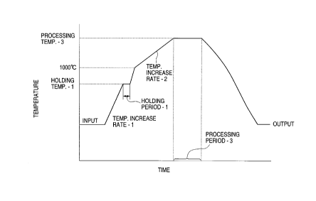
Fig. 1 shows a temperature application schedule of the
heat treatment steps of this embodiment. In Fig. 1,
~temperature increase rate-l" and "holding temperature-1l~
("holding period-1"3 correspond to the heat history
initializing step and the controller nuclei growing step,
respectively. In the steps corresponding to ~'temperature
increase rate-2" and "processing temperature-3~ ("processing
period-3~'), BMDs deposit (grow) stably in the inside of each
wafer and the wafer surface is formed with a DZ layer.
Fig. 2 is a sectional view schematically showing a
silicon wafer produced by this embodiment. A silicon wafer 11
includes an inside BMD concentration adjusted layer 13 and a DZ
layer 12. An intermediate layer (not shown) is usually formed
between the layers 12 and 13.
- 13 -
2171375
Silicon wafers were actually produced according to the
method of this embodiment and a conventional method, and those
wafers were compared with each other.
First, single crystal silicon ingots were produced by
pulling under several different conditions, and sliced into
wafers. Table 1 shows results of oxygen concentration values
measured.
Those wafers were subjected to heat treatments under
processing conditions shown in Table 2. Five wafers were
prepared for each condition and heat-treated together. In the
conventional method, no holding step at 850-980C was performed
in the midst of increasing the temperature.
After the heat treatments, resulting silicon wafers
were subjected to a BMD concentration measurement, results of
which are shown in Table 3.
Table l
Pulling Oxygen concentration O
condition (atoms /cm3 )
A 1.35 x 10!8
B 1.3S x 10l8
C 1.55 x 10'8
D 1.55 x 10l8
E 1.60 x 10!8
F 1.60 x 10~8
- 14 -
Table 2
Condi- ~tmosphere Input Increase llolding llolding Increase Processing Processing
tion temp. rate-l temp. period rate-2 temp.-3 period-3
No. (C) (C/min) (C) (min) (C/min) (C) (hr)
1 H2-100% 700 20 900 20 2 1,200 60
2 H2-100% 800 20 900 20 2 1,200 60
3 H2-100% 700 15 900 20 2 1,200 60
4 H2-100% 700 30 900 20 2 1,200 60
H2-100% 700 20 850 20 2 1,200 60
6 H2-100% 700 20 980 20 2 1,200 60
7 H2-100% 700 20 900 1 2 1,200 60
H2-100% 700 20 900 60 2 1,200 60
9 H2-100% 700 20 900 20 3 1,200 60
H2-100% 700 20 900 20 2 1,100 60
11 H2-100% 700 20 900 20 2 1,250 60
12 H2-100% 700 20 900 20 2 1,200 10
13 H2-100% 700 20 900 20 2 1,200 180
14 Ar-100% 700 20 900 20 2 1,200 60
He-100% 700 20 900 20 2 1,200 60
16 H2-50% 700 20 900 20 2 1,200 60 l~
Ar-50%
CJ~
~able 3
Experi- Wafer Condition ~verage BMD Mnximum BMD Minimum BMD DZ nemarks
ment No. concell~r.~tio concentrntion concentration thickness
No. n (xlOfi cm-l) (xlOC cm~3) (~m)
(xlOC clll-3)
Pl A 1 4.~ 5.0 4.1 9 Invention
P2 B 1 4.6 4.~ 4.2 9 Invention
lll ~1 (No D.0 2.0 13 9 Conv.
holding)
~2 ~1 (No 12 2.0 16 9 Conv.
holdinc3)
P3 C 7 7D 75 79 9 Invention
P4 D 7 75 70 7~ 9 Invention
3 C7 (No 100 55 165 9 Conv.
olding )
n~ D7 (No lD0 100 250 9 Conv.
holding)
PS F1~ 530 500 590 9 Invention
P6 F1~ 570 510 5D0 9 Invention
n5 ~1~ (No 790 2501050 9 Conv.
holding)
nG F1~ (No 570 2501100 9 Conv.
holdinc3 )
P7 C16 D5 7D D9 9 Invention
PD D16 90 ~ 96 9 Invention
n7 ClG (No 15() ~() 220 9 Conv.
llolding ) ~~
IID DlG (No 27() 15()390 9 Conv. C~
llolding )
.
217137~
As seen from Table 3, in the conventional heat
treatments, even with wafers having the same oxygen
concentration at the time of slicing ingots, the BMD
concentration varies by more than 50% and more than several
S times in extreme cases.
In contrast, in the heat treatments of this embodiment,
with wafers having the same oxygen concentration, the BMD
concentration varies by only less than 15%. According to the
embodiment, the variation of the oxygen concentration can be
made as low as 40% in the worst case.
It is expected that this embodiment allows BMDs to be
distributed generally uniformly in the inside of a wafer, that
is, this embodiment can make a variation of the BMD
concentration in the same wafer very small.
According to this embodiment, the BMD concentration in
the inside of a wafer is adjusted by the heat history
initializing step and the controlled nuclei growing step.
Therefore, it becomes possible to produce silicon wafers
exhibiting a superior IG effect and being stable in quality.
Embodiment 2
Fig. 3 is a graph showing a range of conditions for
occurrence of slip defects in a case where a temperature
difference exists in a silicon wafer, in which the horizontal
axis represents the average temperature of a wafer. The part
of the graph above the curve is a slip occurrence range. The
present inventors have found that slips occur at a high
21 7I375
possibility when the temperature distribution in a wafer is
located in the slip occurrence range.
As seen from Fig. 3, as the temperature exceeds
1,000C, the possibility of occurrence of slip defects steeply
increases, that is, slip defects come to appear even with a
small temperature difference in a wafer. Therefore, at a
temperature higher than l,000C, it is necessary to manage the
wafer temperature more strictly.
In view of the above nature of the occurrence of slip
defects, this embodiment employs the following heat treatments
to form a non-defect layer (DZ layer) in a layer to become
device active layers of a silicon wafer. An initial
temperature increase step is performed in which the temperature
is increased in a range of 800C to 1,000C at a rate of 15-
100C/min, then a gradual temperature increase step isperformed in which the temperature is increased at a low rate
in a range of l,000C to 1,300C, and finally a temperature
holding step is performed in which the temperature is kept
constant in a range of 1,100C to 1,300C for not less than 5
minutes.
It is preferable that in the gradual temperature
increase the temperature increase rate be 0.5-10C/min. It is
even preferable that in that step the temperature increase rate
be 1-5C/min.
If the temperature increase rate is lower than 0.5C,
the heat treatment takes so long time that the manufacturing
- 18 -
2171375
cost becomes unduly high. If it is higher than 10C/min, the
temperature difference in a wafer becomes too large to
positively prevent occurrence of slip defects.
If the initial temperature increase step is performed
S at a rate lower than 15C/min, minute nuclei (embryos), which
may cause crystal defects in the inside of a wafer, grow to
enhance the generation of BMDs, disabling formation of a good
non-defect layer. A temperature increase rate higher than
100C/min is not practical because of large heat stress
imparted to a wafer.
As for the temperature holding step, if the holding
temperature is lower than l,000C, the efficiency of outward
oxygen diffusion is too low to allow formation of a good non-
defect layer. If it is higher than 1,300C, B~Ds grow
lS excessively in the inside of a wafer, lowering its mechanical
strength.
It is preferred that the above heat treatments be
performed in an atmosphere including at least one of hydrogen,
helium, and argon.
By performing the above heat treatments, the wafer
surface is formed with a non-defect layer (DZ layer) which is
not thinner than 3 ~m and in which the concentration of oxygen
deposits (BMDs ) is not higher than 103 cm^3. If the DZ layer is
thinner than 3 ~m, a high-quality silicon wafer cannot be
25 obtained because of such problems as leakage in a device
forming step.
-- 1~ --
2171375
The upper limit of the thickness of the DZ layer is set
at about 30 ~m, because if the DZ layer is thicker than about
30 ~m, there occur such problems as lowering of the gettering
effect on the DZ layer of a BMD layer formed in the inside of
a wafer.
It is possible for the above heat treatments to form a
BMD layer in the inside of a silicon wafer. The BMD layer is
a layer that contains oxygen deposits and exhibits the
intrinsic gettering (IG) effect. To form such a BMD layer, it
is desirable that wafers obtained by slicing a single crystal
silicon ingot have an interstitial oxygen concentration Oi of
1.2-1.8 x 10~8 atoms/cm3.
Fig. 4 shows an example of heat treatment steps
according to this embodiment. In Fig. 4, a temperature
increasing step from a furnace input temperature TlC to
1,000C is indicated by "temperature increase rate-1," a
temperature increasing step from 1,000C to 1,200C is
indicated by "temperature increase rate-2," and a temperature
holding step that is performed after those temperature
increasing steps is indicated by "heat treatment.~
Silicon wafers were actually produced by the method of
this embodiment. As comparative examples, silicon wafers were
also produced by changing part of the heat treatment
conditions.
First, silicon wafers having average oxygen contents of
1.3 x 10l3, 1.5 x 10l8 and 1.7 x 10~8 atoms/cm3 (respectively
- 20 -
2171375
denoted by W-A, W-B and W-C) were formed by pulling up single
crystal silicon ingots under different pulling conditions and
slicing those ingots.
Those wafers were subjected to heat treatments shown in
Table 4, in which HT01-HT10 are comparative examples and HTll-
HT38 are examples of this em~odiment.
HT01-HT05 are comparative examples in which the
temperature increase rate was kept constant in a range of 2-
30C/min. HT06 and HT07 are comparative examples in which
temperature increase rate-1 after the wafer inputting was set
at 30C/min and subsequent temperature increase rate-2 was
decreased to 20 or 15C/min. HT08 is a comparative example in
which the processing atmosphere gas was argon rather than
hydrogen. HT09 and HT10 are comparative examples in which
temperature increase rate-l was increased to 40 or 50C/min.
HTll-HT13 are examples of the embodiment in which the
furnace input temperature was set at 600C, 700C and 800C,
respectively. HT14-HT18 are examples of the embodiment which
are the same as HT12 except that temperature increase rate-2
20was set at 0.5, l, 5, 10 and 15C/min, respectively. HT19-HT22
are examples of the embodiment which are the same as HT12
except that temperature increase rate-1 was set at 20, 50, 60
and 80C/min, respectively. HT23-HT26 are examples of the
embodiment which are the same as HT12 except that the
25processing temperature~ was set at 1,100C, l,150C, l,250C
and 1,290C, respectively. HT27 and HT28 are examples of the
2~71375
embodiment which are the same as HT12 except that the process
atmosphere gas was argon and helium, respectively, rather than
hydrogen. HT29-HT33 are examples of the embodiment in which
the heat treatments were conducted in a 2-component or 3-
component gas atmosphere of hydrogen, argon, and helium.
- 22 -
21 7137~
x c
c
Q. a
a) o c~
t~ U H
rr~
l C
C,
-~ OOOOOOOOOO OOOOOOOOOOOO
U` OOOOOOOOOO OOOOOOOOOOOO
U` N N C'~ `1 C'`l N ~ N C~l N N N t'`l N t~ t'~l N N
-I a, o
U~ C
O ~ O ~) Ltl Ll-) U-) t~ N C'`l ~I
~) ~ U
C, ~o
a1 H ~
E~ c~ oooooooooo oooooooooooo
-1 0000000000 000000000000
C~ OOOOOOOOOO OOOOOOOOOOOO
~a s ~ o
ul cl
~
U ~ ~l
C, ~o
H S-l ~
~_ OOOOOOOOOO OOOOOOOOOOOO
H ~ _
O O O O O O O O O ~ ~ ~1
21 7137~
c
~q .,
s~ ~
H
O O O O O O O O O O O Lr~ O
C
1, ~, _
ooooooo o o o o ooooo
7 0 ~ U~ ~ O O O O o o O o o o O o
~ ~V
~ a) o
a)
U~ C
a) I
c ~, a
C ~0
o H ~1 --
V
d~ C ooooooo o o o o ooooo
~-1 0 0 0 0 0 0 0 0 0 o o O O O O O
~D t' ooooooo o o o o ooooo
a) c Q,--
~ t~ r C~ O
a) _
u~ C
a) I ~ O O O O O O O O O O O O O O O O
~ ~ U
C ~o
H S-l --
~Q~_ OOOOOOO O O O O OOOOO
~
H ~) _
S~ +++++.
O o o o O o O O
¢ I X :C ~ X ~
Z ~ ~ ~ X X _ X ~ _ X
-- 24 --
21~137~
Results of the experiments for the wafers W-A, W-B and
W-C are shown in Tables 5-7, respectively. As seen from Tables
5-7, even if the oxygen concentration of wafers is varied, the
DZ layer thickness and the degree of occurrence of slips have
almost no variations. Further, in any of the examples, the DZ
layer was not thinner than 3 ~m.
Even when the furnace input temperature was varied
between 600C to 800C, no slip occurred (HT11-HT13).
Even when temperature increase rate-1 (to 1,000C) is
as high as 30C/min, the occurrence of slip defects was
prevented by lowering subsequent temperature increase rate-2
(HT14-HT18).
Further, even when temperature increase rate-1 (to
1,000C) was increased from 20C/min to 80C/min, no slip
defect occurred or slip defects occurred only slightly (HT19-
HT22).
In Tables 5-7, the "scale of slips" was judged
according to JIS H0609-1994, "Method of Observing Crystal
Defects of Silicon Due to Selective Etching." Specifically,
"small" means that slips occur at only one location on a wafer
observed and the number of slips is not greater than 10.
"Medium" means that slips occur at only one location and the
number of slips is greater than 10, or slips occur at a
plurality of locations and the total number of slips is not
greater than 50. ~Large~ means that slips occur at a plurality
of locations and the total number of slips exceeds 50.
21.7137~
When the "processing temperature" was varied between
1,100C and 1,290C, the DZ layer became thicker as the
temperature increased. Although slips became more liable to
occur as the temperature increased, their scale was very small
(HT23-HT26).
Even with an atmosphere of helium or argon, or an
atmosphere in which hydrogen was mixed with helium and/or
argon, a DZ layer was formed in the same manner as with an
atmosphere consisting only of hydrogen and no slips occurred
(HT27-HT33).
When the "processing period" was increased from 5 to
240 minutes, the DZ layer thickness merely increased without
occurrence of slips (HT34-HT38).
- 26 -
21 71375
Table 5
Wafer Conditions DZ layer Scale o~
type thickness slips
(~m)
W-A HTO1 9 Large
HT02 9 Large
HT03 9 Medium
HT04 lO Small - -
HT05 10 None
HT06 9 Large
HT07 9 Medium
HT08 9 Medium
HTO9 9 Medium
HT10 9 Large
~-A HT11 10 None
HT12 10 None
HT13 10 None
HT14 12 None
HT15 11 None
HT16 10 None
HT17 10 None
HT18 9 Small
HT19 10 None
HT20 10 None
HT21 10 Small
HT22 10 Small
HT23 6 None
HT24 8 None
HT25 18 None
HT26 27 Small
HT27 9 None
HT28 9 None
HT29 9 None
HT30 10 None
HT31 10 None
HT32 10 None
HT33 10 None
HT34 3 None
HT35 5 None
HT36 7 None
HT37 15 None
HT38 21 None
- 27 -
21 7I37~
Table 6
Wafer Conditions DZ layer Scale of
type thickness slips
(~m)
W-B HTO1 9 Large
HT02 9 Large
HT03 9 Medium
HT04 9 None
HT05 . 10 None
HT06 9 Large
HT07 9 Medium
HT08 9 Medium
HTO9 9 Medium
HT10 9 Large
.
r- W-B HT11 10 None
HT12 10 None
HT13 10 None
.HT14 11 None
HT15 10 None
HT16 10 None
HT17 10 None
HT18 g None
HT19 10 None
HT20 10 None
HT21 10 None
HT22 10 Small
HT23 6 None
HT24 8 None
HT25 18 Small
HT26 26 Small
HT27 g None
HT28 9 None
HT29 9 None
HT30 10 None
HT31 10 None
HT32 10 None
HT33 10 None
HT34 3 None
HT35 5 None
HT36 7 None
HT37 15 None
HT38 21 None
- 28 -
217137S
Table 7
~afer Conditions DZ layer Scale of
type thickness slips
(~m)
W-C HT01 8 Large
HT02 9 Medium
HT03 9 Medium
HT04 9 None
HT05 10 None
HT06 9 Large
HT07 9 Small
HT08 9 Small
HT09 8 Medium
HT10 8 Large
W-C HT11 9 None
HT12 9 None
HT13 9 None
HT14 10 None
HT15 10 None
HT16 9 None
HT17 9 None
HT18 9 None
HT19 10 None
HT20 10 None
HT21 9 None
HT22 9 Small
HT23 5 None
HT24 7 None
HT25 17 Small
HT26 25 Small
HT27 9 None
HT28 9 None
HT29 9 None
HT30 10 None
HT31 10 None
HT32 10 None
HT33 10 None
HT34 3 None
HT35 5 None
HT36 7 None
HT37 14 None
HT38 19 None
- 29 -
217137~
As is apparent from the above experiments, this
embodiment can produce, efficiently and at a low cost, a high-
quality silicon wafer whose surface is formed with a DZ layer
of more than 3 ~m in thickness and is substantially free of
slip defects.
It is noted that this embodiment is applicable to
silicon wafers which have been produced by the FZ (float zone)
method and have a relatively small oxygen content. Also in
such a case, the embodiment can modify the wafer surface by
forming a DZ layer while further reducing the oxygen
concentration in the surface layer.
Embodiment 3
It is noted that oxygen concentration values that will
appear in this embodiment are ones according to the conversion
coefficients of Old ASTM.
First, a description will be made of general behavior
of BMDs in heat-treating a wafer. According to the classical
nuclei formation theory, a BMD grows or shrinks such that
supersaturated oxygen is attached to or removed from a an
oxygen cluster serving as a homogeneous nucleus. Whether a BMD
grows or shrinks/disappears depends on the critical nucleus
radius at a time point concerned. The critical nucleus radius
is determined by the size of a BMD, the temperature, and the
oxygen concentration. The critical nucleus radius is larger
for a higher temperature. Where a wafer is kept at a certain
temperature, a BMD larger than its critical nucleus radius at
- 30 -
21 71375
that temperature continues to grow while a BMD smaller than its
critical nucleus radius shrinks/disappears.
By applying the above knowledge to the wafer
manufacture, the present inventors have found that wafers
suitable for manufacture of highly integrated devices can be
produced by properly controlling the BMD behavior, and
completed this aspect of the invention.
This embodiment is characterized in that a silicon
wafer having an interstitial oxygen concentration Oi of 1.4-1.8
x 10l8 atoms/cm3 is subjected to a temperature holding step
which is performed at a temperature between 1,100C and 1,300C
for 1 minute to 48 hours in an atmosphere including at least
hydrogen and an inert gas, and that a temperature increase rate
in a range of the room temperature to 900C is set at 15-
100C/min and a temperature increase rate in a range of 900Cto the holding temperature is set at 1-15C/min.
As for the temperature holding step, if the holding
temperature is lower than 1,100C, the BMD concentration cannot
be made low. If it exceeds 1,300C, the safety and the
reliability of the manufacturing apparatus may not be assured.
If the duration of the temperature holding step is
shorter than 1 minute, the BMD concentration cannot be made low
enough to ensure the intended effects of the invention. Even
if the temperature holding step continues for more than 48
hours, no added effects can be attained.
- 31 -
2l7l37~
As for the temperature increasing step (room
temperature to 900C), by setting the temperature increase rate
at not less than 15C/min, the effective increase rate of the
critical nucleus radius can be made higher than the effective
S growth rate of BMDs. As a result, the critical nucleus radius
can be larger than radii of a considerable part of existing
BMDs, which therefore shrink. However, since the temperature
increase rate is relatively high and the temperature increasing
step lasts for only a short period, the number of BMDs that
completely disappear during this step is not large (almost no
BMDs disappear under certain conditions). Naturally the number
of BMDs large enough to be detected is decreased to some
extent.
It is preferable that the temperature increase rate in
the range of the room temperature to 900C be set not lower
than 20C/min. It is even preferable that the above
temperature increase rate be set not lower than 30C/min. By
employing such a high temperature increase rate, the
concentration of large (or detectable) BMDs can further be
reduced.
In the range of 900C to the holding temperature, if
the temperature increase rate exceeds 15C/min, the BMD
concentration becomes so low that the gettering effect becomes
insufficient and slips become liable to occur, which will cause
problems in a device forming step. If the temperature increase
rate is lower than 1C/min, the BMD concentration becomes too
2l 7I 375
high to ensure the intended effects of the invention.
Resulting wafers will not ~e suitable for formation of highly
integrated devices.
It is preferable that the temperature increase rate in
the range of 900C to the holding temperature be set at 5-
10C/min. In this case, the above-described advantage of the
invention can be enhanced.
Referring to Fig. S, solid line a indicates an example
of a heat treatment process of this embodiment and chain line
b indicates an example of a conventional heat treatment
process.
By performing the above heat treatments, this
embodiment can form a DZ layer which is not thinner than 10 llm
(as measured from the surface) and in which the concentration
of BMDs not smaller than 20 nm in diameter is not more than 103
cm~3, and a bulk portion having an oxygen deposit concentration
of 1 x 103 cm~3 to exp(9.21 x 10-l3 x Oi + 3.224) cm~3. Such
silicon wafers correspond to a region A + B + C in the graph of
Fig. 6.
It is preferable that the ~3MD concentration be from 1
x 103 cm~3 to the smaller one of 1 x 108 cm~3 and exp(9.210 x 10-l8
x Oi + 3.224) cm~3 (region A + B in Fig. 6). It is even
preferable that the BMD concentration be not higher than
exp(5.757 x 10-l3 x Oi + 3.224) cm~3 (region A in Fig. 6).
A wafer having a BMD concentration within the above
range exhibits the gettering function. Further, a superior DZ
21 7I37~
layer (non-defect layer) is formed in a surface layer to become
device active layers, and sufficient mechanical strength is
assured.
It is preferred that substantially no BMDs exist in a
surface DZ layer. The reasons why the BMD concentration range
in a DZ layer is specified in the above manner are that the
m;nimllm detectable BMD size of the currently available
measuring devices is 20 nm, and that it is inappropriate to
call a state with a BMD concentration higher than 103 cm~3 "non-
defective"; that is, such a wafer adversely affects thecharacteristics of devices formed thereon.
A description will now be made o Examples 1-5
according to this embodiment and Comparative Examples 1-4.
Wafers used in Examples 1-5 and Comparative Examples 1-4 are
ones that were cut out of silicon ingots produced by the
Czochralski method and subjected to ordinary mirror-polishing.
The wafers were of the N-type, and had surface orientation of
(100) and a resistivity of 1-1,000 Q-cm. The initial
interstitial oxygen concentration O, was 1.4-1.74 x 10l8
atoms/cm3. A vertical heat treatment furnace was used in which
the heat insulation was improved and the amount of heat
generated by a heating source was increased.
Example 1
Among the above-mentioned wafers, wafers having a
concentration O of 1.7 x 10l8 atoms/cm3 were subjected to a heat
treatment (holding step) of 1,200C and l hour in a lO0
- 34 -
21 7I375
hydrogen atmosphere. The temperature increase rate was set at
30C/min between 700C and 900C and at 10C/min between 900C
and 1,200C. The temperature decrease rate was set at 3C/min.
Example 2
Wafers having Oi of 1.61 x 10l8 atoms/cm3 were subjected
to heat treatments in the same manner as in Example 1.
Example 3
Wafers having Oi of 1.51 x 10l8 atoms/cm3 were subjected
to heat treatments in the same manner as in Example 1.
Example 4
Heat treatments were conducted under the same
conditions as in Example 1 except that the temperature increase
rate was set at 20C/min between 700C and 1,000C and at 10C
between l,000C and 1,200C.
Example 5
Wafers having O. of 1.43 x 10l8 atoms/cm3 were subjected
to heat treatments in the same manner as in Example 1.
Comparative Example 1
Among the above-mentioned wafers, wafers having a
concentration Oi of 1.7 x 10l8 atoms/cm3 were subjected to a heat
treatment (holding step) of 1,200C and 1 hour in a 100%
hydrogen atmosphere. The temperature increase rate was set at
10C/min both between 700C and 1,000C and between 1,000C and
1,200C. The temperature decrease rate was set at 3C/min.
Comparative ExamDle 2
2171~75
Wafers having Oi of 1.61 x 10l8 atoms/cm3 were subjected
to heat treatments in the same manner as in Comparative Example
1.
Comparative Example 3
Wafers having Oi of 1.51 x 10l8 atoms/cm3 were subjected
to heat treatments in the same manner as in Comparative Example
1. . :
Comparative Example 4
Wafers having OL Of 1.43 x 10l8 atoms/cm3 were subjected
to heat treatments in the same manner as in Comparative Example
1.
The concentration of BMDS occurring in the respective
wafer ((110) cross-section) that had been subjected to the heat
treatments of Examples 1-5 and Comparative Examples of 1-4 was
measured by infrared tomography. The minimum detectable B~D
size of the infrared tomography method employed was 20 nm. The
detection limit of the BMD concentration depends on measurement
regions. In the measurements concerned, the measurement regibn
was a rectangular parallelepiped region which includes a wafer
surface area of 4 ~m x 200 ~m and has a depth of 185 ~m. In
this case, the detection limit of the BMD concentration was 6.8
x 106 cm~3. Under these conditions, the thickness of a DZ layer
as defined in the invention (a layer in which the concentration
of BMDS not smaller than 20 nm is not more than 103 cm~3)
corresponds to a depth at which a BMD is first detected in a
217137~
classical field of view when the detection is started from the
surface.
Measurement results and heat treatment conditions are
shown in Tables 8 and 9. Fig. 6 is a graph showing a
relationship between the initial oxygen concentration and the
BMD concentration. The "DZ layer thickness" in the tables
means a depth at which a BMD not smaller than 20 nm is first
detected when the detection is started from the wafer surface
(A DZ layer does not contain a BMD that is not smaller than 20
nm).
As seen from Tables 8 and 9 and Fig. 6, this embodiment
can form a good DZ layer even with wafers in which the initial
oxygen concentration O. is high. Further, the B~D
concentration in a bulk portion can be reduced.
That is, this embodiment can form a DZ layer (non-
defect layer) which is not thinner than 10 ~m (as measured from
the wafer surface) and in which the concentration of B~Ds not
smaller than 20 nm in diameter is not more than 103 cm~3, and a
bulk portion having an oxygen deposit concentration of 1 x 10³
cm~3 to exp(9.21 x 10-l8 x l + 3.224) cm~3.
Thus, according to this embodiment, a layer to become
device active layers can be rendered non-defective and the
concentration of BMDs in the vicinity of such a layer can be
reduced, so that it becomes possible to produce devices having
superior characteristics at a high yield.
- 37 _
~17137~
In contrast, in the wafers of Comparative Examples 1-4
which were subjected to the heat treatments under the
conditions that are out of the ranges of the embodiment, the
BMD concentration is higher for a higher initial oxygen
concentration. Although a DZ layer is formed even in
Comparative Examples 1-4, BMDs are formed in the inside of a
wafer at a high concentration, which means that a large number
of BMDs exist in the vicinity of a DZ layer. A large number of
BMDs existing in the vicinity of a wafer surface layer to
become device active layers will proba~ly deteriorate the
device characteristics. In addition, the mechanical strength
of a wafer is lowered.
Table 8
Ex. 1 Ex. 2 Ex. 3 Ex. 4 Ex. 5
Marking in Fig. 6 o o o o o
tXlol8 atoms/cm3) 1.70 1.61 1.51 1.70 1.43
Atmosphere 100% hydrogen gas
Processing temp. l,200C
Processing period l hour
Increase rate 30 30 30 20 30
(C/min)
Decrease rate 3 3 3 3 3
(C/min)
DZ layer thickness (~m) 80 90 130 70 150
Bulk BMD concentration 1.7 1.7 1.7 1.7 1.3
(x107 cm~3)
- 38 -
2t71375
Table 9
Comp. Comp. Comp. Comp.
Ex. 1 Ex. 2 Ex. 3 Ex. 4
Marking in Fig. 6 o o o o
Oi (x10l8 atoms/cm3) 1.70 1.61 1.51 1.43
Atmosphere 100% hydrogen gas
Processing temp. 1,200C
Processing period 1 hour
Increase rate (C/min) 10 10 10 10
Decrease rate (C/min) 3 3 3 3
DZ layer thickness (~m) 10 10 10 15
Bulk BMD concentration 170 1~0 75 50
(x107 cm~3)
According to this embodiment, even with a wafer having
a high initial oxygen concentration, a good non-defect surface
layer can be formed and the BMD concentration in a bulk portion
can be made low. Therefore, it becomes possible to produce
high-quality silicon wafers for highly integrated devices at a
high yield.
Further, by using silicon wafers produced according to
this embodiment, highly integrated devices having superior
characteristics can be produced at a high yield.