Note: Descriptions are shown in the official language in which they were submitted.
W095/07559 PCT~S94/09812
~ ~1 714~4
GANG MODULAR JAC~
FIELD OF THE INVENTION
The present invention generally relates to electrical
connectors, and more particularly to improved configurations of
5 modular jacks which are used for connecting a telephone set to
a telephone line.
BACKGROUND OF THE INVENTION
Conventionally, modularjacks having fundamental parts
thereof standardized in conformance with the FCC standard or
the like are used to connect telephone sets to telephone lines.
The modular jack of this kind generally has a box-shaped
housing with a plug inserting opening on the front surface of
the housing. When the telephone set is connected to the
telephone line, a plug which is provided on an end of the
telephone line is inserted into the plug inserting opening. A
plurality of contact pins are held in the housing so that one
end of each of the contact pins projects from the bottom of the
housing to constitute a terminal part and the other end of each
of the contact pins projects within the plug inserting opening
of the housing to constitute a contact part. The modular jack
is placed on a printed circuit board which is secured to a main
telephone body, in such a manner that the plug inserting
opening is exposed to the outside of the telephone body. The
terminal part constituted by the contact pins projecting from
the bottom of the housing is soldered to respective circuit
W095/07~59 PCT~S9~/098~2
2 -
patterns on the printed circuit board within the telephone
body.
Because of the dimen.sional variation of the jack
caused by plastic shrinkage, the resultant position of the
terminal part of a conventional modular jack is somewhat
different from the nominal po.sition as designed. For this
reason, it is difficult and time-consuming to solder the
terminal part of the modular jack to the printed circuit board.
In addition, owing to the wicking strength induced in the
contact area between the plastic housing and the contact pin,
the flux migrates up along the contact pin to the contact part
during fluxing and soldering processes so that the conductivity
of the contact part is lowered. Furthermore, since sockets of
conventional telephone sets are separate from the modular jacks
15 where the sockets may be used as a DC power socket, antenna
socket or an interface socket for another device, it is time-
consuming to assemble the sockets and the modular jacks onto
the telephone sets. Consequently, there is a need for
practical and economical configurations of modular jacks which
can overcome the disadvantages described above.
SUMMARY OF THE INVENTION
Accordingly, it is the general object of the present
invention to provide a novel and useful configurations of
modular jacks in which the problems described heretofore are
25 eliminated.
A specific object of the present invention is to
provide an electrical connector in which the terminal part of
a contact pin is more precisely positioned.
According to a first aspect of the present invention,
a plurality of recesses are located close to terminal slots at
both sides to rectify dimensional variation caused by plastic
shrinkage.
According to a further aspect of this invention, a
terminal slot is constructed by two V-shape protrusions at its
35 neck area so that the round terminal part of the contact pin is
more precisely positioned in the housing.
217l4~4
W095/07559 PCT~S9~/098~2
_ - 3 -
Another specific object of the present: inVentiOIl is
to eliminate the wicking of the flux.
According to a second aspect of the invention, a flux
trap is provided at the contact area between the plastic
housing to eliminate the wicking of the flux.
According to a third aspect of the present invention,
a modular jack is integrated with a socket.
These and other objects, advantages and features of
the present invention will be more fully understood and
appreciated by reference to the following detailed description
when read in conjunction with the accompanying drawings.
BRIEF DESCRIPTION OF THE DRAWINGS
Fig. 1 is a perspective view showing an embodiment of
a modular jack in accordance with the present invention;
Fig. 2 is a cross section of the modular jack shown
in Figure 1 along a line II-II;
Fig. 3 is a bottom view of the modular jack of the
present invention;
Fig. 4 is an enlarged view of a terminal slot shown
20 in Fig. 3; and
Fig. 5 is a cross section of the modular jack shown
in Figure 1 along a line V-V.
DETAILED DESCRIPTION OF THE PREFERRED EMBODIMENTS
Figure 1 depicts an embodiment of a modular jack
25 in accordance with the present invention. A preferred
embodiment of a modular jack of the present invention mainly
comprises a housing 1, a socket 2, at least one plug inserting
opening 3, two mounting legs 4 (Figure 2), and two mounting
ears 7. The housing 1 in the preferred embodiment is made of
30 formed plastics and i5 provided with a plug inserting opening
3 on the front surface thereof to receive a plug provided at
rthe one end of a telephone line. A plurality of slots 6 are
formed on the upper surface and the bottom surface of the
housing 1. T~ese slots 6 are disposed in parallel relationship
35 to each other for accommodating contact pins 5.
~==:
WO95/07S~9 ~ PCT~S9~/098~2
-- 4
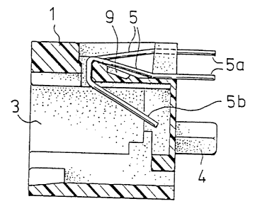
Figure 2 is a cross section of the modular jack along
a line II-II in Figure 1, showing ~he structure of the plug
inserting opening 3 and the contact pins 5. The modular jack
is provided with several contact pins 5, each of which runs
5 within a channel in the housing 1. Each contact pin 5 is held
firmly within the channel and the slot 6. One end of a contact
pin 5 projects from the bottom of the housing 1 to constitute
a terminal part 5a for electrically conducting with a printed
circuit board and the other end of a contact pin 5 projects
10 within the plug inserting opening 3 of the housing 1 to
constitute a contact part 5b for electrically conducting with
the plug provided at one end of the telephone line. When the
modular jack is mounted onto the printed circuit board by
soldering, the flux, owing to the wicking strength induced in
the contact area between the plastic housing and the contact
pin, migrates up along the contact pin 5 to the contact part 5b
during fluxing and soldering processes so as to lower the
conductivity of the contact part 5b.
According to an embodiment of a modular jack of the
20 present invention, the a cavity 9 is defined in the contact
area between the plastic housing and the contact pin to
function as a flux trap. The cohesion force of the wicked flux
will be eliminated when the wicked flux migrates up to the
cavity 9. Therefore, the problem of flux wicking is overcome,
and the conductivity of this embodiment of the modular jack in
accordance the present invention is much improved.
Referring to Figures 3 and 4, in an embodiment of a
modular jack of the present invention, the housing 1 is
provided with two diamond shaped mounting legs 4 at the bottom
and two mounting ears 7 at the side walls. These diamond
shaped mounting legs 4 are oriented so that the major axis of
the first leg is oriented perpendicular to the axis of the
second leg and these legs are adapted to be inserted into
corresponding holes in the printed circuit board. The mounting
35 ears 7 engage with the corresponding slits in the telephone set
when the modular jack is secured to the telephone.
WO9~/07559 Z 7 ~1 4~ PCT~S9~/09842
- 5
According to an embodiment of a modular jack of tLle
present invention, a plurality of recesses 8 are located close
to terminal slots 6 at both sides to rectify dimensional
variation caused by plastic shrinkage. The terminal slots 6
5 with the rectifying recesses 8 result in more precise
positioning of the terminal part 5a of the contact pins 5 than
the conventional art. The resultant position of the terminal
part 5a of the contact pins 5 is closer to the nominal position
as designed. As a consequence, the modular jack can be more
easily and precisely mounted onto and soldered to the printed
circuit board.
According to an embodiment of a modular jack of the
present invention, terminal slots 6 are constructed by two V-
shape protrusions 6a at their neck area so that the round
terminal part 5a of a contact pin 5 is more precisely
positioned in the housing 1. The unique two V-shape
protrusions 6a along with the rectifying recesses 8 also result
in more precise positioning of the terminal part 5a of contact
pins 5 than the conventional art.
~s shown in Figure 1, an embodiment of a modular jack
in accordance with the present invention is integrated with a
socket 2. The socket may be configured to be suitable for a
number of different functions, for example, as a DC power
socket, antenna socket or interface socket for another device.
In an embodiment of a modular jack in accordance with the
present invention, the socket is configured for use as a DC
power socket. Figure 5 is a cross section of the modular jack
along a line V-V in Figure 1, showing this configuration of
socket 2, i.e., as a DC power socket in accordance with the
30 present invention. With the integrated socket 2, a telephone
set can be assembled faster.
While only particular embodiments of the present
invention have been shown and described herein, it will be
appreciated that modifications thereof may be readily made
thereto by those skilled in the art. We, therefore, intend by
the appended claims to cover the modifications which fall
within the true spirit and scope of the invention.