Note: Descriptions are shown in the official language in which they were submitted.
2172 21~ 95-152 CA
SPECIFICATION
HIGH PERFORMANCE CARD EDGE CONNECTOR
Field of the Invention
The present invention relates to electrical
connectors for printed circuits and more particularly to a
high density, low impedance card edge connector useful in
high frequency circuits.
Description of the Prior Art
Card edge connectors are widely used for
connecting printed circuit cards, called daughtercards, to
printed circuit boards or motherboards. A typical card
edge connector includes an insulating housing with a card
edge receiving slot and numerous cavities receiving
electrical terminals. The terminals include board contacts
extending downward from the housing and card contacts that
engage conductive pads on the edge of a card inserted into
the slot. The housing is mounted on the motherboard with
the board contacts soldered to conductive regions of the
motherboard. The card edge connector removably receives
the daughtercard and the terminals provide conductive paths
between conductive pads on the card and conductive regions
of the board.
In order to achieve improved performance, faster
operating speeds and increased circuit density are
important trends in digital electronic circuits using
printed circuits. For example, microprocessors operate at
ever increasing frequencies and communicate with ancillary
devices such as memory, display drivers and the like over
wide channels with increasing numbers of parallel
connections. These trends result in problems in the design
of connectors used with such circuits.
The goal of high circuit density may be met with
2172219
95-152 C~
closely spaced terminals having relatively small cross
sectional areas. The requirement for high frequency
operation results in the need for low impedance in order to
accommodate fast digital pulse rise times and wide
bandwidth. But close circuit spacing can result in
increased crosstalk due to capacitive coupling and can
result in increased impedance due to long and/or narrow
signal paths. In addition, at high frequencies, shielding
from external interference may be desirable. Known card
edge connector designs have not been entirely effective in
meeting these several and sometimes conflicting goals
without high cost and undesirable complexity.
Summary of the Invention
A principal object of the present invention is to
provide an improved high performance card edge connector.
Other and more specific objects are to provide a connector
with high circuit density and low impedance; to provide a
connector suitable for use with high frequency digital
signals; to provide a connector in which crosstalk is
minimized; to provide a connector having interference
shielding characteristics; and to provide an improved
connector overcoming disadvantages of card edge connectors
used in the past.
In brief, in accordance with the present
invention there is provided a card edge connector for a
removable printed circuit card having a mating edge with a
plurality of conductive pads. The connector includes an
insulating housing with elongated top and bottom walls and
elongated spaced apart side walls. A plurality of
transverse cavities extend between the side walls. An
elongated slot in the top wall receives the mating edge of
the circuit card. The slot intersects the cavities and
divides them into similar, aligned cavity portions at
opposite sides of the slot. A plurality of ground and
signal terminals are received in the cavity portions, and
each of the terminals includes a mounting portion for
. 217221~
-
95-152 CA
holding the terminal in one of the cavity portions and a
contact portion for engaging one of the contact pads upon
insertion of the mating edge into the slot. The card edge
connector is characterized by a single one of the ground
terminals being disposed in each of a group of spaced apart
first cavity portions, and a plurality of the signal
terminals being disposed in each of a group of second
cavity portions, each of the second cavity portions being
adjacent one of the first cavity portions.
2172219
-
95-152 C~
Brief DescriPtion of the Drawings
The present invention together with the above and
other objects and advantages may best be understood from
the following detailed description of the preferred
embodiments of the invention illustrated in the drawings,
wherein:
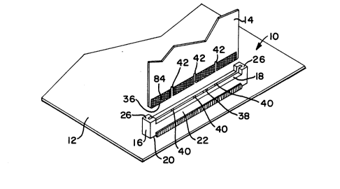
FIG. 1 is an isometric view of a high performance
card edge connector constructed in accordance with the
present invention used for interconnecting a printed
circuit motherboard and a printed circuit daughtercard;
FIG. 2 is an enlarged fragmentary horizontal
sectional view of the connector taken along the line 2-2 of
FIG. 3;
FIG. 3 is a sectional view of the connector taken
along the line 3-3 of FIG. 2;
FIG. 4 is a sectional view of the connector taken
along the line 4-4 of FIG. 2;
FIG. 5 is a fragmentary enlarged elevational view
of part of the daughtercard of FIG. 1;
FIG. 6 is a fragmentary enlarged plan view of
part of the motherboard of FIG. 1;
FIG. 7 is a view like FIG. 3 illustrating another
embodiment of the invention, and is a sectional view taken
along the line 7-7 of FIG. 9;
FIG. 8 is a sectional view of the connector of
FIG. 7, taken along the line 8-8 of FIG. 9;
FIG. 9 is an enlarged fragmentary horizontal
sectional view of the connector taken along the line 9-9 of
FIG. 7;
FIG. 10 is a fragmentary enlarged elevational
view of part of a daughtercard used with the connector of
FIG. 7; and
FIG. 11 is a fragmentary enlarged plan view of
part of a motherboard used with the connector of FIG. 7.
~ 217221~
._
95-152 CA
Detailed Description of the Preferred Embodiments
Having reference now to the drawings, FIG. 1
illustrates a card edge connector 10 constructed in
accordance with the principles of the present invention
together with a printed circuit motherboard 12 and a
printed circuit daughtercard 14. In a typical application
for example, the board 12 may be a motherboard of a
computer or other electronic device incorporating digital
electronics, and card 14 may be a smaller printed circuit
board or daughterboard having electronic devices such as
memory or the like. Connector 10 is mounted on the board
12 and the card 14 is releasably inserted into the
connector 10 in order to establish electrical connections
between the board 12 and card 14.
The structure of the connector 10 is seen in
FIGS. 1-4. It includes an insulating housing 16 formed of
molded plastic including an elongated top wall 18, a bottom
surface 20, and elongated, opposed side walls 22 and 24.
The ends of the housing 16 are provided with raised guide
portions 26. The housing may be provided with standoffs
and mounting pegs (not shown) extending down from the
bottom wall 20 to hold the housing 16 on the board 12 until
it is permanently attached in a soldering operation with
bottom wall 20 parallel to the board surface. These
features are disclosed for example in U.S. patent
5,259,768.
An array of numerous terminal receiving cavities
28 extend transversely between the side walls 22 and 24.
The cavities are separated by barrier walls 30 of the
housing 16. The upper portions of the cavities 28 are
closed by the top wall 18 and the lower portions of the
cavities open through the bottom surface 20. The housing
16 includes an elongated, central internal mounting rail
32. Terminal spacer projections 34 extend outwardly from
the side walls 22 near the bottom of the housing 16.
The daughtercard 14 includes a mating edge 36.
The housing 16 includes an elongated slot 38 formed along
2172219
-
95-152 CA
the center of the top wall 18 for receiving the mating edge
36. The guide portions 26 aid in inserting the mating edge
36 into the slot 38. The housing 16 includes keys or
transverse webs 40 extending across the slot 38 and
received in keyways or channels 42 in the mating edge 36 to
provide a positioning or keying function. The slot 38
intersects the cavities 28 and the walls 30, and the
cavities are divided into opposed, transversely aligned
cavity portions 28A and 28B on opposite sides of the slot
38. All of the cavities 28 are identical to one another,
and all of the portions 28A and 28B are also identical
except for orientation with respect to the slot 38. A
bottom wall 39 of the slot 38 is defined by portions of the
barrier walls 30.
Electrical connections are made between the
motherboard 12 and the daughtercard 14 by signal terminals
44 and 46 and by ground terminals 48 received in the
cavities 28. The terminals 44, 46 and 48 are formed from
conductive sheet metal, for example by blanking, stamping
and forming, and in the illustrated arrangement are loaded
into the cavities 28 through the bottom surface 20.
Each ground terminal 48 includes a base portion
50 that generally coincides with bottom surface 20 when the
terminal is in place. A board contact or tail portion 52
extends down from the base portion 50 for connection to a
conductive region of the board 12. A large area panel
portion 54 extends up from the base portion 50, and a
flexible resilient spring arm portion 56 extends from the
panel portion 54. The spring arm portion 56 terminates in
a card contact portion 58 that is located within the slot
38 in the path of an inserted mating edge 36 of card 14.
A mounting portion or arm 60 secures the ground terminal 48
in place by frictionally receiving the side wall 22 or 24
between the arm 60 and the panel portion 54. Arm 60 is
received between a pair of the lugs 34.
Each "inner" signal terminal 44 includes a base
portion 62 that generally coincides with bottom surface 20
~ 2172219
95-152 CA
when the terminal is in place. A board contact or tail
portion 64 extends down from the base portion 62 for
connection to a conductive region of the board 12. A
flexible resilient spring arm portion 66 extends from the
base portion 62. The spring arm portion 66 terminates in
a card contact portion 68 that is located within the slot
38 in the path of the inserted mating edge 38 of card 14.
A mounting portion or finger 70 is frictionally received in
an aperture in the rail 32 in order to secure the signal
terminal 44 in place.
Each "outer" signal terminal 46 includes a base
portion 72 that generally coincides with bottom surface 20
when the terminal is in place. A board contact or tail
portion 74 extends down from the base portion 50 for
connection to a conductive region of the board 12. A leg
portion 76 extends up from the base portion 72, and a
flexible resilient spring arm portion 78 extends from the
leg portion 76. The spring arm portion 78 terminates in a
card contact portion 80 that is located within the slot 38
in the path of an inserted mating edge 36 of card 14. A
mounting portion or arm 82 secures the signal terminal 46
in place by frictionally receiving the side wall 22 or 24
between the arm 82 and the leg portion 76. Arm 82 is
received between a pair of the lugs 34.
High contact density is achieved with the
connector 10 by mounting more than a single signal contact
in the cavity portions 28A or 28B. As seen in FIGS. 3 and
4, a signal contact 44 and a signal contact 46 are mounted
side by side in a single cavity portion. The terminals 44
and 46 are electrically independent from one another
because they are spaced apart and not in contact with one
another. As a result, two independent electrical signals
may be conducted through a single cavity portion 28A or
28B.
Impedance control, signal isolation and crosstalk
reduction are achieved by interspersing the ground
terminals 48 among the signal terminals 44 and 46. Every
2172219
95-152 CA
other cavity portion 28A and every other cavity portion 28B
is provided with a ground terminal 48. The remaining
alternate cavity portions 28A and 28B are each provided
with a pair of signal terminals 44 and 46. On both sides
S of the slot 38 there is a pattern of alternating ground and
signal terminals. A part of this continuing pattern is
seen in FIG. 2. Preferably the patterns are offset on
opposed sides of the slot 38 so that in each cavity 28 a
pair of signal terminals 44 and 46 are directly opposite a
single ground terminal 48.
Within the pattern of terminals of the connector
10, each signal terminal pair 44, 46 is sandwiched between
a flanking pair of ground terminals 48 and is also aligned
with an opposed ground terminal 48 on the opposite side of
the slot 38. This geometry provides some of the advantages
of a coaxial transmission path where a signal conductor is
surrounded by a ground conductor, but with significantly
greater density and significantly lower material and
assembly costs.
One factor in limiting the cost of the connector
10 is the modularity of the design. Each identical cavity
portion 28A or 28B of each identical cavity 28 can
accommodate either a single ground terminal 48 or a pair of
signal terminals 44 and 46 without any modification of the
housing structure. All of the signal terminals 44 are
disposed near the longitudinal center of the housing 16 and
can be mounted on either side of the slot 38 in either a
cavity portion 28A or a cavity portion 28B by insertion of
the finger portion 70 into the central mounting rail 32.
Either a signal terminal 46 or a ground terminal 48 can be
mounted in any cavity portion 28A or 28B by engagement of
the arm portion 60 or the arm portion 82 with a side wall
22 or 24.
The ground terminals 48 and signal terminals 44
and 46 are configured to reduce crosstalk by creating
preferential couplets between the signal terminals 44 and
46 and the ground terminals 48 rather than directly between
2172219
95-152 CA
signal terminals 44 and 46. As seen in FIGS. 3 and 4, the
large area, continuous panel portions 54 of the ground
terminals 48 have peripheries or silhouettes that surround
or overlie the spring arm portions 66 of signal terminals
44 as well as the leg portions 76 and the spring arm
portions 78 of the signal terminals 46. Base portions 50
also overlie base portions 62 and 72.
Substantially the entire signal current paths
through the signal terminals 44 and 46 are aligned between
large area portions of the immediately adjacent ground
terminals 48. The relatively large area and mass of the
ground terminals 48 achieves a ground plane effect and
reduced ground inductance. In addition, the ground
terminals 48 are separated from the pairs of signal
terminals 44 and 46 by barrier walls 30. These walls are
part of the housing 16 and are a molded, dielectric plastic
material. In contrast the terminals 44 and 46 of each pair
of signal terminals are separated by air. The dielectric
housing material increases the coupling of each signal
terminal 44 and 46 to the adjacent ground terminal, while
the air separation between signal terminals minimizes the
cross coupling between signal terminals 44 and 46.
Card contact portions 68 of the signal terminals
44 are arranged in two lines at opposite sides of the slot
38 and parallel to the bottom wall 20. These lines are
equidistant from the bottom wall 20 and are relatively
close to the bottom 39 of the slot 38. Card contact
portions 80 of the signal terminals 46 are also arranged in
two lines at opposite sides of the slot 38 and parallel to
the bottom wall 20. These lines are equidistant from the
bottom wall 20 and are located above the lines of card
contact portions 68. Card contact portions 58 of the
ground terminals 46 are also arranged in two lines at
opposite sides of the slot 38 and parallel to the bottom
wall 20. These lines are equidistant from the bottom wall
20 and are located above the lines of card contact portions
68 and 80.
21722~19
95-152 CA
The ground terminals 48 provide an interference
shielding effect because the ground card contact portions
58 are more elevated than the signal card contact portions
68 and 80. The ground paths are arrayed like a canopy or
5umbrella around the signal current paths and act to shield
the signal current paths from electromagnetic interference.
The card contact portions of the terminals 44, 46
and 48 are arrayed in a high density configuration. The
card contact portions 68 and 80 of each pair of signal
10terminals 44 and 46 are vertically spaced apart and are
aligned in the same vertical plane. The card contact
portion 58 of the transversely opposed ground terminal 48
lies in the same vertical plane. The card contact portions
48 of the two flanking ground terminals 48 are
15longitudinally spaced from this vertical plane by a
distance equal to the pitch of the terminals within the
housing 10, i.e. the distance between centerlines of
cavities 28.
As seen in FIG. 5, the card 14 includes a contact
20pad array 84 configured to mate with the card contact
portions 58, 68 and 80. A first line of signal contact
pads 86 lies along the mating edge 36. Pads 86 are
contacted by the card contact portions 68 of signal
terminals 44 when the card 14 is inserted into slot 38. A
25second line of signal contact pads 88 lies above pads 86.
Pads 88 are contacted by the card contact portions 80 of
signal terminals 44 when the card 14 is inserted into slot
38. A third line of ground contact pads 90 lies above pads
86 and 88. Pads 90 are contacted by the card contact
30portions 58 of ground terminals 48 when the card 14 is
inserted into slot 38. One of the two surfaces of the card
14 is seen in FIG. 5. The opposite side is similar except
that the pads are displaced longitudinally by a distance
equal to the connector pitch with signal pads 86 and 88 on
35one surface of the card aligned with a ground pad 90 on the
opposite surface.
The board contact or tail portions 52, 64 and 74
21 72219
95-152 CA
of the terminals 48, 44 and 46 are arrayed to maximize
circuit density not only within the connector 10 but also
at the interface with the motherboard 10. The board
contact portions 74 of signal terminals 46 are in two
parallel longitudinal lines at the opposite sides of the
housing 16. The board contact portions 64 of signal
terminals 48 are in two parallel longitudinal lines located
near the center of the housing 16. The board contact
portions 52 of the ground terminals 48 are in two parallel
lines between the board contact portions 74 and 64. The
lines of the board contact portions are equally spaced
apart across the width of the connector 10, and preferably
the spacing is equal to the connector pitch.
A matching array 92 of conductive regions on the
board 12 is seen in FIG. 6. Central lines of conductive
regions 94 are engaged by board contact portions 64 of
signal terminals 44. Outer lines of conductive regions 96
are engaged by board contact portions 74 of signal
terminals 46. Intermediate lines of conductive regions 98
are engaged by board contact portions 52 of ground
terminals 48. The uniform transverse spacing equal to the
connector pitch produces the uniformly staggered array 92
seen in FIG. 6 and permits high signal density.
In the illustrated arrangement, the conductive
regions 94, 96 and 98 are plated-through holes in the board
12, and the board contact portions 52, 64 and 74 are solder
tail or pin contacts suitable for insertion into the holes
where they are soldered in place by a known flow soldering
process. Alternatively, other contacts such as surface
mount foot contacts could be used and the conductive
regions 94, 96 and 98 could be plated areas on the board
surface to which the contacts are soldered by known surface
mount soldering techniques.
FIGS. 7-11 illustrate an alternative embodiment
of the invention in the form of an electrical connector
110. Similar reference characters used with connectors 10
and 110 identify similar structural features.
11
217221~
95-152 CA
In connector 10, alternate cavity portions 28A
and 28B contain ground terminals 48 or signal contacts 44
and 46. Thus, as seen in FIG. 2, the ground and signal
current paths alternate and each signal terminal pair 44,
46 is sandwiched between a pair of ground terminals 48. In
the connector 110 (FIG. 9), two adjacent cavity portions
28A or 28B receive signal terminal pairs 44, 46, and the
pair of signal terminal cavities is sandwiched between
cavities 28A or 28B containing ground terminals. The
coupling of signal terminals to ground is not as effective
as with the arrangement of connector 10, but the signal
capacity or circuit density is increased. Every pair of
signal terminals 44 and 46 is immediately adjacent to a
ground terminal 48 and effective coupling to ground is
achieved for every signal path.
The pattern of board contact portions 52, 64 and
74 of connector 110 differs from that of the connector 10.
Thus, as seen in FIG. 11, the pattern of conductive regions
or plated through holes 94, 96 and 98 in the motherboard 10
is altered. In addition, due to the differences in the way
the terminals are arrayed, the arrangement of signal
contact pads 86 and 88 and of ground contact pads 90 on the
daughtercard 12 is also altered.
As best seen in FIGS. 7 and 8, the ground
terminals 48 of the connector 110 have mounting portions or
arms 60' that are longer than the portions or arms 82 of
the signal terminals 46. Arms 60' extend toward the top
wall 18 beyond the arms 82 and beyond the spacers 34.
Connector 110 includes a conductive metal shield 112 having
a top wall 114 and side walls 116 terminating in an
enlarged skirt 118. The skirt 118 engages the ends of the
arms 60' so that the shield is electrically connected to
ground through numerous electrically parallel paths
providing extremely low resistance and inductive impedance.
An alternative configuration for retaining the
terminals in the housing is shown in FIGS. 7 and 8. The
housing is slightly modified and is particularly useful for
2172219
-
95-152 CA
applications in which the terminals are loaded into the
cavity portions 28A, 28B by hand rather than with
automation equipment. - Rail 32 of the connector 110 has
downwardly extending portions 32A located at each cavity
portion 28A or 28B where a ground terminal 48 is mounted.
These portion block access of the mounting portions 70 of
terminals 44 to the aperture in the mounting rail 32. The
resulting keying effect prevents inadvertent mounting of
signal terminals in a cavity portion intended for a ground
terminal 48.
While the present invention has been described
with reference to the details of the embodiments of the
invention shown in the drawing, these details are not
intended to limit the scope of the invention as claimed in
the appended claims.