Note: Descriptions are shown in the official language in which they were submitted.
.. 2172563
1
SUBSCRIBER LINE INTERFACE AND POWER CIRCUIT
FIELD OF THE INVENTION
The invention relates to telephone Subscriber Loop Interface Circuits (SLIC)
providing so-called BORSCHT functions.
BACKGROUND OF THE INVENTION
A subscriber line interface circuit (or SLIC) serves as an interface between a
subscriber telephone line and a digital switching system. A SLIC provides what
is
commonly referred to as BORSCHT functions as well as a digital to analog
conversion
between the digital switching system and telephone line. The BORSCHT functions
include Battery feed, Overvoltage protection, Ringing, Supervision, Codec,
Hybrid and
Testing. It appears, however, that the present technology is directed to
moving the
BORSCHT functions to the serving terminal of the outside loop plant which
provides
the connections between the telephone lines extending to a customer's
telephone station
sets and a local or central switching system. That is, the serving terminal is
the
apparatus which connects the telephone "drop" line extending to a telephone
subscriber's premises and the local or central office switching system.
We have recognized, however, that prior art SLIC circuits do not actually
provide all BORSCHT functions. For example, such circuits are not capable of
generating the ringing voltage (R) and, therefore, have to rely on an external
(e.g.,
central office) ringing generator to supply the ringing voltage to a
subscriber's line.
Accordingly, if a SLIC circuit supposedly providing all BORSCHT functions were
moved to a serving terminal of the outside plant, then a ringing generator
would also
have to be moved to the serving terminal to provide the ringing voltage, when
needed,
to the telephone drop lines connecting to the serving terminal. It can be
appreciated
then that prior art SLIC circuits are indeed limited.
2172563
2
SUMMARY OF THE INVENTION
Accordingly, an object of the present invention is to provide a subscriber
line circuit
which truly provides all of the BORSCHT functions and does not rely on an
external ringing
generator to do so. We achieve this result and advance the relevant art by
recognizing that
supervisory and ringing signals occur in some sort of sequence and, therefore,
do not have to
be generated simultaneously. Based on this recognition, we have developed, in
accord with
the invention, a circuit which truly implements all of the BORSCHT functions
and includes a
power section that generates each of the supervisory signals, e.g., -48 volts
and -24 volts, and
alerting signal, e.g., ringing signal, in turn and as required.
In accordance with one aspect of the present invention there is provided
apparatus for
interfacing a telephone station set with transmission facilities comprising:
means for
outputting different sequences of first, second and third control signals
respectively indicative
of when said station set is on-hook, off hook and when an associated telephone
switch has
received an incoming call for said station set; and means for independently
generating first
and second supervisory signals and a ringing signal in an order corresponding
to the
sequential order of a current one of said sequences of said control signals,
in which the levels
of said first, second and third control signals are respectively indicative of
the levels of the
first and second signals and the ringing signal.
In accordance with another aspect of the present invention there is provided
apparatus
comprising: means for generating in sequence first, second and third control
signals; and
means, responsive to receipt in turn of a current one of said first, second
and third control
signals, for independently generating as a function of said one of said first,
second and third
control signals a corresponding signal selected from a group of signals
including an off hook,
ringing and on-hook signals, in which the level of said one of said first,
second and third
control signals is indicative of the level of the independently generated
signal.
BRIEF DESCRIPTION OF THE DRAWINGS
FIG. 1 is a block diagram of a subscriber line interface circuit in which the
principles
of the invention may be practised; and
FIG. 2 illustrates a sequence of signals that the subscriber line interface
circuit
generates in accord with an aspect of the invention.
A
2a 2 1 7 2 5 6 3
DETAILED DESCRIPTION
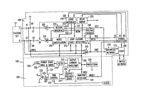
Turning to FIG. l, Subscriber Line Interface and Power (SLIP) circuit 100
includes
power section 300 and telephony section 200 for providing each of the BORSCHT
functions.
Power section 300, more particularly, includes power stage 305 which generates
each of the
supervisory signals, e.g., -48 volts and -24 volts, and alerting signal, e.g.,
ringing signal,
responsive to the type of control signal that it receives from Pulse Width
Modulation Control
(PWMC) circuit 330 via lead 331. Power stage 305 supplies the generated signal
(designated
VREG in the FIG.) to conventional high-frequency filter 310. Filter 310
"smoothes out"
VREG by removing a high-frequency noise component from VREG and supplies the
result to
a conventional current sense/limit circuit 315. Current sense/limit circuit
315, in a
conventional manner, monitors the level of current on bus 350 to "sense" the
presence of an
A
2172563
3
inadvertent error condition, e.g., a ground fault. That is, circuit 315
compares a
predetermined error level with the level of current that VREG is supplying to
bus 350.
If the latter level meets or exceeds the former level, then circuit 315
concludes that a
ground fault is present on bus 350 and supplies an inhibit signal to PWMC
circuit 330.
Circuit 330, responsive to the inhibit, supplies a "shut down" signal to power
stage 305
via lead 331. Power stage 305, in turn, stops generating VREG.
Output voltage sense circuit 340, on the other hand, divides the level of VREG
appearing on bus 350 by a predetermined factor, e.g., a value of 100, and
supplies the
result to PWMC circuit 330 via lead 341. For example, if VREG is, e.g., -48V (-
24V),
then circuit 340 supplies a -480 millivolt (-240 mv) signal to circuit 330.
Circuit 330, in
turn, compares the level of the signal that it is receiving via lead 341 with
the level of
the reference signal (VAR REF) that it is receiving from voltage follower
circuit 335 via
lead 326. Circuit 330 then adapts the signal that it is outputting to lead 331
to account
for the difference, thereby providing a regulating function to adapt VREG to a
level
specified by the level of VAR REF. The path from bus 350 to output voltage
sense 340
and thence to PWMC circuit 330 via lead 341 thus constitutes a linear feedback
arrangement for regulating the level of VREG. (It is noted that PWMC circuit
330 may
be similar to the teaching set forth in the publication Studies in Electrical
a_nd lectro is
~n_gin ring 45 - Pulse Width Modulared (per r ~~ Rp~~ by V. Quercioli,
published by Elsevier, 1993, pp. 5-10, which is incorporated herein by
reference; and
power stage 305 may be similar to the teaching set forth in the Unitrode
A,Rplications
Handbook 1985-1986, Application N U-76 - Flyback and Boost Switching regulator
Design Guide, published by Unitrode Corporation, 5 Forties Road, Lexiton, Ma.
02173,
pp. 86-94, which is also incorporated herein by reference.)
Briefly referring to telephony section 200, loop closure detector circuit 235
monitors the dc. loop resistance across the Tip (T) and Ring (R) leads
extending to
telephone station set S 1. As is well-known, the resistance of such a loop is
typically
very large (thousands of ohms) or relatively small (possibly several hundred
ohms or
less) when station set S 1 is respectively on-hook or off hook. When station
set S 1 is
2172563
4
on-hook (also referred to herein as a steady state), loop closure detector
circuit 235 thus
detects a very large resistance across the T and R leads. In that case,
circuit 235 outputs,
for example, -480 millivolts dc. to lead A extending to one input of follower
circuit
335. Follower 335 supplies that voltage level to PWMC circuit 330 as VAR REF.
Circuit 330, in turn, supplies to lead 331 a signal having, in accord with an
aspect of the
invention, a duty cycle corresponding to the level of VAR REF, e.g., when VAR
REF is
-480 millivolts dc., then PWMC circuit 330 outputs a signal having an
appropriate duty
cycle to lead 331. That is, a duty cycle selected in accord with the teachings
disclosed
in the aforementioned references. Power stage 305, in turn, converts the
voltage level
that it receives via lead 304 into a signal having a level controlled by the
duty cycle of
the signal that it receives via lead 331. That is, power stage 305 converts
the supply
voltage level, e.g., +12 V, supplied via lead 304 into a -48V do signal. Power
stage 305
then outputs the result to filter 310 as VREG, as mentioned above.
When station S 1 goes from an on-hook state to an off hook state, loop-closure
detector circuit 235 then detects a relatively low resistance across the T and
R leads and
changes the level of the signal that it is outputting to lead A. For example,
circuit 235
outputs -240 millivolts dc. to lead A. PWMC circuit 330, responsive to the
change in
VAR REF, outputs a signal to lead 331 having a duty cycle corresponding to the
new
VAR REF, as mentioned above. Power stage 305, in turn, converts the voltage
level, or
signal, supplied to lead 304 to -24 Vdc and outputs that signal as VREG.
Power stage 305 also generates a ringing signal that is supplied as VREG to
ring
lead R via resistor RR. Specifically, when the telephone switch (not shown)
forwards
an incoming call to station set S1, it also transmits a signaling message
indicative
thereof. The signaling message includes information identifying (a) the
channel that is
assigned to the call, (b) calling telephone number, (c) called telephone
number, etc. In
response to receipt of the message via codec 275, channel processor 280
directs logic
interface circuit 220 via logic leads BO and B 1 to transmit a ringing signal
to station S 1
to alert the user thereat to the incoming call. Processor 280 does this by
setting the d.c.
signals on leads BO and B1 to represent one of four states (codes), e.g., 00,
O1, 10 or 11.
2112563
It is assumed herein that state 00 represents a steady state (e.g., a low
power scan state)
and 11 represents the ringing state. Accordingly, processor 280 applies a
logic one (e.g.,
+5 vdc) to lead BO and to lead B 1. Logic interface circuit 220, responsive to
that logic
state, notifies circuit 235 via lead 231 to transmit a ringing signal to
station S 1. Circuit
5 235, in turn, reshapes the clock signal, e.g., +5V clock signal, that it
receives from
processor 280 via lead RCLK into a -1.7 V peak trapezoidal signal varying at a
20 Hz
rate and supplies that signal to PWM control circuit 330 via follower circuit
335. PWM
control circuit 330 then supplies a signal having a duty cycle varying
according to the
new VAR REF to lead 331. Logic interface circuit 220 also causes contact SR to
operate to isolate amplifier 210 from the ring lead. (It is noted that contact
SR is
representative of an electronic device capable of effecting a switching
function, e.g., a
FET device.)
Power stage 305, in response to the signal supplied via lead 331, converts the
supply voltage from lead 304 into a -170V peak trapezoidal signal varying at a
20 Hz
rate (ringing signal) and outputs the signal to filter 310 as VREG, which is
supplied to
ring lead R via circuit 315 and resistor RR. When the user at station S 1
answers the eall
by causing station S 1 to go off hook, the level of current in the T and R
loop circuit
increases as a result of the decrease in the resistance of the loop. This
increase in
current is detected by Ring Trip Detector 345, which then changes the logic
state of the
NRDET lead extending to processor 280.
Processor 280, responsive to the signal on lead NRDET being at a logic state
of
one, changes the logic state of leads BO and B 1 to O1 (indicative of station
S 1 being in
an off hook state), which, in turn, causes logic interface circuit 220 to
rescind its request
for a ringing signal and allow contact SR to resume a normally closed state.
In addition,
loop closure circuit 235 outputs a -240 my signal to lead A, thereby
indirectly causing
power stage 305 to output a -24V signal as VREG, as discussed above.
It is seen from FIG. 1 that telephony section 200 of SLIP 100 also includes
conventional amplifiers 205 and 210 for supplying analog signals, e.g., voice
signals,
etc., to the T and R leads. More specifically, codec 275 receives digital
versions of such
- 2112563
6
analog signals from the telephone network, converts the digital signals to
analog signals
and then supplies the resulting analog signals to receive interface circuit
215 via
balanced network 270. Receive interface circuit 215 then transmits the signals
over the
T and R leads via amplifiers 205 and 210, respectively, which are a.c. coupled
to the T
and R leads via capacitors CT and CR, respectively. Receive interface circuit
215, more
particularly, comprises a differential pair that provides a do voltage level
translation
between the codec signal and the TIP and RING signal. Circuit 215 supplies the
resulting analog signal to the T and R for transmission to station S 1 .
Circuit 215 also
provides a gain adjustment between the codec and the T and R leads based on
system
requirements.
Ax amplifier 245, on the other hand, detects analog signals traveling in the
opposite direction, i.e., speech signals originating at station S1, and
supplies such
signals to codec 275 via balanced network 270 and transmission path XMT. AX
amplifier 245, more particularly, is a differential amplifier which senses the
differential
voltage level across the T and R leads, scales the differential voltage by a
predetermined
factor of, for example, a value of three (3), and outputs the result to
transmit path XMT
for transmission to codec 275. Codec 275 includes an analog-to-digital
converter
circuit, which converts analog signals (e.g., speech signals) that are
received via path
XMT into digital signals for transmission to the public switched network. The
signal
that amplifier 245 outputs to path XMT is also supplied to voltage divider
circuit 240.
Voltage divider circuit 240 essentially controls the gain of the feedback path
including
receive interface circuit 215 such that the gain of the feedback path
synthesizes the
equivalent output impedance presented to station S 1. That is, the feedback
loop
synthesizes the expected loop impedance, e.g., either 600 or 900 ohms. To say
it
another way, we create a positive feedback path having a gain of less than one
such that
the equivalent differential impedance may be multiplied (by the gain of the Ax
Amp
245, voltage divider 240 and RCV interface circuit 215) to match the expected
impedance.
2112563
Telephony section further includes noise cancellation circuit 230 which is
designed in a conventional manner to sense any noise signal of a relatively
small voltage
that is a component of VREG and generate a model of the noise component so
that it
can be subtracted from the analog signal (voice signal) that receive interface
circuit 220
supplies to AR amplifier 210. Basically, noise cancellation circuit 230
synthesizes a
current source (i.e., a Norton equivalent circuit equal to the VREG noise
signal divided
by RR and 180 degrees out of phase with the noise signal) that generates a
signal that is
somewhat equal to the level of the noise signal but 180 degrees out of phase
with that
signal. Accordingly, the signal generated by circuit 230 cancels the noise
signal "riding"
on VREG.
Loop closure circuit 235 includes a differential voltage level comparator
circuit
to monitor the d.c. resistance across the T and R leads so as to detect when
station S 1 is
either in an on-hook and off hook state, as discussed above. In addition to
controlling
the level of the signal that it outputs to lead A to signify a Station S 1 on-
hook or off
hook state, circuit 235 also outputs a logic one (+5 vdc) or logic zero
(ground) to lead
NLC to notify processor 280 of the state of station S1. Circuit 235 thus
notifies
processor 280 whenever station S 1 goes from an on-hook to an off hook state
and vice-
versa. Processor 280, responsive thereto, sends a signaling message requesting
service
to the telephone network via codec 275. The telephone network, in turn,
returns dial
tone, as is done conventionally. Processor 280 also sends a signaling message
to the
telephone network when station S 1 goes from off hook to an on-hook state as
tracked by
the logic state on lead NLC. The telephone network may then respond to the
latter
signaling message by terminating any existing telephone connection extending
to station
S1.
The fault detection section of circuit 235 includes two differential voltage
level
comparators designed to detect a predetermined voltage drop, e.g., 36 Vdc,
across
resistors RR and RT, respectively. The voltage drop is indicative of a fault
condition
and its presence causes circuit 235 to activate conventional relay driver
circuit 225.
That is, the output of each differential voltage level comparator is supplied
to an OR
2172563
s
circuit whose output activates driver circuit 225. When activated, relay
driver 225
operates an associated relay (not shown), which, in turn, operates normally
closed
contacts X1 and X2 to disengage SLIP 100 from the loop extending to station
Sl.
Channel processor 280 may operate relay driver circuit 225 via lead B2 to
isolate SLIP
100 from station S 1 so that maintenance tests may be performed on SLIP 100.
Logic interface 220 provides an interface between SLIP 100 and processor 280.
Specifically, logic interface circuit 220 is a conventional combinatorial
circuit which
converts a logic state to one of n functions supplied at the output. In the
instant case,
processor 280 controls the binary input via leads B 1 and B2, which may assume
one of
four logic states, namely 00, O1, 10 and 1 l, as mentioned above. State 00 is
the steady
state when station set S 1 is on-hook as also mentioned above. During state
00, circuits
215 and 230 are "powered down" via leads 221 and 222 to conserve power. The
power
up state is O 1 and occurs when station S 1 is in the off hook state. State 10
is not used
and state 11 is the ringing state, which causes circuit 220 to call for a
ringing signal via
lead 231 and operate contact SR as mentioned above.
FIG. 2 is one example of a sequence of signals (voltage levels) that power
section 300 generates in response to respective control signals received from
telephony
section 200, in which the sequence illustrates an on-hook signal level 'a'
that is supplied
to station S 1 as a result of telephony section 200 detecting that station S 1
is on-hook.
Telephony section 200 may also direct power stage 300 to independently
generate a
ringing signal illustrated at 'f in response to receipt of an indicator
indicating that the
network has an incoming call for station S 1. Section 200 may also direct
power stage
300 to generate an off signal 'c' instead of the ringing signal in response to
station S 1
going off hook. The FIG. also shows that power stage 300 generates a on-hook
signal
'f as a result of telephony section 200 detecting that station S 1 has
returned to the on-
hook state. Although the FIG. does not indicate so, the next signal in the
sequence
could be an off hook signal 'f that is generated as a result of station S 1
going off hook
to request service, e.g., placing a telephone call. It is noted that the
signals shown in
2172563
9
FIG. 2 would also be illustrative of the control signals generated by
telephony section
200 at lead 'A' as long as such signal levels were decreased accordingly.
The foregoing is merely illustrative of the principles of the invention. Those
skilled in the art will be able to devise numerous arrangements, which,
although not
explicitly shown or described herein, nevertheless embody those principles
that are
within the spirit and scope of the invention.