Note: Descriptions are shown in the official language in which they were submitted.
2172761
Pc 664 1
OPTICAL TELECOMMUNICATION METHOD PROVIDING A TRANSMITTING AND
RECEIVING SERVICE CHANNEL
D e s c r i p t i o n
The invention relates to an optical telecommunication system. More
particularly it refers to a telecommuncation 'system having an
optical-fibre transmitting line in which an independent channel for
service communications comprising a data-transmitting unit and a
data-receiving unit for transmission/reception over said service
channel is provided.
Optical-fibre telecommunication systems adapted to enable signal
transmission for communication over long distances usually provide, in
addition to channels intended for communication signals and put at the
users' disposal, also an independent channel adapted to enable
transmission of service signals.
Such service signals can be of various types, for example command or
control signals for apparatus disposed along the line, such as
repeaters or amplifiers, or communication signals between the
maintenance staff acting at a line point and an intermediate station
or terminal of the line itself.
For service signals a restricted transmission band as compared with
the band of the communication channels is usually sufficient. An
overall transmission speed of 300 Kbit/s, in,the case in which service
signals are coded on a single digital channel is deemed sufficient,
for example.
In an optical-fibre telecommunication system a remedy for signal
attenuation along the fibres is necessarily provided by periodically
amplifying the signals. The use of optical amplifiers disposed at
regular intervals along the transmission line has proved to be
convenient.
2172761
Pc 664 2
Such amplifiers, that can be made of optical fibres doped with a
fluorescent substance and submitted to optical pumping, are capable of
amplyfing the signals without converting them to an electric form.
In these lines it is impossible to insert and extract signals into and
from the fibre along which they are transmitted by means of known
electronic apparatus, because signals are available in the optical
form even close to the amplifiers.
US Patent 5,113,459 in the name of the same applicant describes an
optical telecommunication system optionally provided with optical
amplifiers along the line, in which insertion and extraction of the
service channel takes place by dichroic couplers.
Also provided in this system are receiving and emitting units
connected to the dichroic couplers, adapted to receive optical service
signals from the line, convert them to electric signals and
electronically amplify them, and to receive the amplified electric
signals, convert them to optical signals at the wavelength of the
service channel and send them to the line, respectively.
In order to carry out separation between the signals by means of
dichroic couplers, the wavelength of the service channel has been
selected considerably different from that of the communication
channels. In addition, for minimizing attenuation for the service
channel, this wavelength has been selected substantially coincident
with or to a small distance from a minimum of the spectral attenuation
curve of light in the optical fibre.
In the case in which the telecommunication signal wavelength is
substantially included between 1500 and 1600 nm (the so-called "third
window" for silica-based optical fibres) and the service channel
wavelength is included in the so-called "second window", for
silica-based optical fibres located in the vicinity of the relative
attenuation minimum at about 1300 nm, the attenuation to which the
service signals are submitted is much greater than that relating to
i ..
2172761
Pc 664 3
the communication channels.
In fact, at the second window wavelengths, the attenuation coefficient
for silica-glass optical fibres usually in use has a value typically
included between 0.37 and 0.41 dB/km, against a typical value of about
0.2 dB/km for wavelengths within the third window.
The length of the line portion included between two amplifiers or
between one of the end stations and one of the amplifiers is given by
the maximum acceptable attenuation at the wavelengths of the
communication channels, in turn linked to the maximum available gain
at those wavelengths.
With the optical amplifiers presently in use this maximum gain is
about 25-30 dB.
The overall attenuation value at the wavelength of the service channel
along the portion between two amplifiers may therefore reach values
higher than 50 dB, for example.
In order to generate the radiation to be used for transmission of the
service channel, the use of semiconductor lasers is provided.
Semiconductor lasers with emission at the wavelength of the second
window have a typical output power of about 1 mW (0 dBm). Lasers
having a greater output power are undesirable due to their high costs.
Taking into account the reduction of the laser output power in time
and aging of the passive optical components along the transmission
line, a further power reduction at the receiver of about 8 dB can be
expected.
The problem exists therefore of transmitting digital signals, in
particular service signals, along an optical communication line and
receiving them with a sufficiently low error rate, in the presence of
a limited power at the receiver.
2172761
Pc 664 4
The present invention in one aspect consists of a digital optical
telecommunication method comprising the steps of:
- receiving a first electric signal carrying a piece of information at
an optical transmission station and generating a digital modulated
optical signal at a predetermined wavelength, corresponding to said
electric signal;
- feeding said modulated optical signal to an optical-fibre line
having a predetermined unitary-attenuation value at said wavelength;
- receiving said modulated optical signal transmitted from said
optical-fibre line to a given optical-power level, at an optical
receiving station, converting it to an electric form and thereat
generating a second digital electric signal;
characterized in that:
- said step of generating a modulated optical signal comprises coding
said piece of information of said first electric signal in a sequence
of elementary information units univocally associated with said piece
of information, said units following one after the other according to
a first predetermined cyclic time rate, and
- said step of generating a second digital electric signal comprising
detecting in said converted signal, an electric signal having a second
cyclic time rate higher than said first cyclic time rate and
recognizing in the detected signal, the phase of an electric signal at
said first time rate by comparing a received sequence of elementary
information units with at least one reference sequence and verifying
the correspondence of result in said comparison at a given condition.
Preferably said second time rate is a multiple of said first time
rate.
In a preferential version, said step of generating a modulated optical
signal comprises generating a third digital electric signal having
said second time rate, starting from said sequence of elementary
information units following one after the other according to a
predetermined first time rate. Said modulated optical signal can be
generated to advantage by modulating the emission of a
coherent-radiation source, by means of said third digital electric
217.?761
PC 664 5
signal. Advantageously, said third digital electric signal can be
generated by phase- modulating a carrier having said second time rate.
Preferably said step of converting said received optical signal to an
electric form comprises detecting said received optical signal,
converting it to an electric signal, filtering said electric signal
and amplifying said filtered signal.
Preferably said reference sequence has said first time rate.
In a particular embodiment, said step of recognizing in the detected
signal, the phase of an electric signal at said first time rate
comprises:
- generating a timing signal at said first time rate and with a random
phase;
- determining, within each period of said timing signal at said first
time rate, the leading edges of said electric signal with said second
time rate that are not simultaneous with the leading edge of the
timing signal;
- counting the leading edges determined in the first and second halves
of said period, using opposite signs respectively;
- adding up the results of the above counting over several consecutive
periods;
- comparing said sum with at least one predetermined value;
= adjusting the phase of said timing signal to said first time rate on
exceeding of said value.
Preferably, said step of generating a second electric signal comprises
recognizing, during each period of said first time rate, an
information unit in a sequence of elementary information units of the
detected electric signal.
In a particular embodiment, said step of receiving said first electric
signal comprises receiving a predetermined number of tributary digital
electric signals with a third time rate lower than said first time
rate and multiplexing them to form a digital electric signal at said
2 17~7~1
Pc 664 6
first time rate.
Advantageously, said particular embodiment comprises the steps of
extracting timing signals at said third time rate from said second
digital electric signal and reconstructing digital electric signals of
same number as said tributary electric signals, starting from said
second digital electric signal and based on said timing signals at
said third time rate.
In a particular embodiment said predetermined wavelength is included
between 1200 nm and 1400 nm.
In a particular solution, said predetermined unitary-attenuation value
is included between 0.37 dB/km and 0.41 dB/km.
The present invention in a second aspect consists of a digital optical
telecommunication method comprising the following steps:
- coding in a differential form, one digital electric signal at a
first time rate from an input port;
- modulating, by said coded signal, the phase of a carrier at a second
time rate which is a multiple of the first time rate;
- modulating by said carrier, the emission of a laser at a
predetermined wavelength;
- feeding the signal emitted from the laser to one end of an
optical-fibre line; ,
- receiving said optical signal at the other end of said optical-fibre
line;
- detecting said optical signal by converting it to an electric
signal;
- amplifying said electric signal;
- filtering said amplified electric signal so as to remove the
spectral components external of a band centered on said second time
rate;
- converting said filtered signal to a digital form;
- generating a timing signal at said second time rate, in timed
relation with said digitalized signal;
21727'61
Pc 664 7
- sampling said signal in a digital form based on said timing signal
at said second time rate;
- operating a differential demodulation of said sampled signal;
- generating a reconstructed digital signal at said first time rate;
- feeding said reconstructed digital signal to an output port;
characterized in that said operation of generating a reconstructed
digital signal at said first time rate comprises the following steps:
- generating a timing signal at said first time rate and with a random
phase;
- determining, within each period of said timing signal at said first
time rate, the leading edges of said demodulated signal that are not
simultaneous with a leading edge of said timing signal;
- counting the leading edges determined in the first and second halves
of said period, using opposite signs respectively;
- adding up the results of the above counting over several consecutive
periods;
- comparing said sum with at least one predetermined value;
- adjusting the phase of said timing signal to said first time rate on
exceeding of said value.
The present invention in a third aspect consists of an optical
telecommunication system comprising:
- an optical transmitting station, adapted to receive a first electric
signal at a first frequency and generate a modulated optical signal
corresponding to said first electric signal, said optical signal
having a predetermined wavelength;
an optical receiving station, adapted to receive said modulated
optical signal and thereat generate a second electric signal at said
first frequency, comprising means for converting said optical signal
to an electric form;
- an optical-fibre line joining said transmitting station and said
receiving station, by transmission of said optical signal;
characterized in that:
- said transmitting station comprises modulation means for said first
electric signal at a second frequency greater than said first
frequency,
2172761
PC 664 8
- said receiving station comprises:
a detection circuit comprising an optical detector of predetermined
sensitivity, adapted to generate a third electric signal at said
optical signal;
a demodulation circuit, comprising:
* a recognition circuit for recognizing the phase of said third
electric signal, and
* a decision circuit, controlled by said recognition circuit, adapted
to generate said second electric signal at said first frequency,
wherein the Bit Error Rate (BER) is better than 10-5, the power of the
optical signal entering said receiving station being lower than a
predetermined optical power smaller than said predetermined
sensitivity.
In a particular embodiment said predetermined wavelength is included
between 1200 and 1400 nm.
In a preferential solution said predetermined optical power is at
least 6 dBm lower than said predetermined sensitivity.
In a preferential embodiment, said first frequency is not less than
200 KHz.
Preferably said second frequency is a multiple of said first
frequency.
The present invention in a fourth aspect consists of an optical
telecommunication system comprising at least one telecommunication
signal-emitting station and one telecommunication signal-receiving
station, one optical-fibre line joining said transmitting and
receiving stations and at least one optical amplifier, means for
admitting optical service signals and means for extracting optical
service signals to and from the optical fibre of the line
respectively, which means comprises at least one emitting and/or
receiving unit for optical service signals, which unit is adapted to
receive from the optical line and/or emit towards the same, service
I i ...
2172761
PC 664
9
signals consisting of communication or control signals electrically
supplied to or extracted from the unit itself, in the form of optical
signals having a service wavelength remarkably different from the
wavelength of the telecommunication signals, which unit is associated
with a related optical coupler connected along the line, adapted to
couple the optical service signals at the inside of the line fibre
and/or extract said signals from the latter, at least one means for
admitting or extracting optical service signals being associated with
at least one optical amplifier,
characterized in that this optical-signal emitting and/or receiving
unit comprises:
- an optical emitting station, adapted to receive said communication
or control signals, generate a modulated optical signal including said
communication or control signals and having said service wavelength,
and senfl said optical signal into a respective associated optical
coupler;
- an optical receiving station, adapted to receive an optical signal
at said service wavelength from a respective associated optical
coupler and thereat generate said electric communication or control
signals, which station comprises means for converting said received
optical signal to an electric form;
wherein said optical emitting station comprises:
- means for generating a first electric signal at a first frequency,
including said communication or control signals,
and wherein said optical receiving station comprises:
- a detection circuit comprising an optical detector adapted to
generate a second electric signal at said received optical signal;
- a demodulation circuit, comprising:
* a recognition circuit for recognizing a phase in said second
electric signal;
* a decision circuit, controlled by said recognition circuit, adapted
to generate a third electric signal at said first frequency,
comprising said communication or control signals supplied to the
emitting and/or receiving unit;
* a separation circuit, adapted to generate said electric
communication or control signals supplied to the emitting and/or
2172761
''- PC 664 10
receiving unit, starting from said third electric signal.
More details will be apparent from the following description, with
reference to the accompanying drawings, in which:
- Fig. 1 is a diagram showing an optical transmitting unit according
to the invention;
- Fig. 2 is a diagram of a frame used in the device of the invention;
- Fig. 3 is a diagram of the first section of the optical receiving
unit according to the invention;
- Fig. 4 is a diagram of the second section of the optical receiving
unit according to the invention;
- Fig. 5 is a diagram of a phase-locked loop used in the device of
Fig. 4;
- Fig. 6 is a diagram of a line terminal according to the invention;
- Fig. 7 is a diagram of an optical telecommunication system according
to the present invention;
- Fig. 8 is a diagram of the configuration adopted during an
experiment;
- Fig. 9 is an eye diagram relating to the optical signal received
during the experiment;
- Figs. 10A to 1OF are eye diagrams relating to the optical signal
received during the experiment for different optical powers at the
receiver;
- Fig. 11 is a diagram of the BER depending on the optical power at
the receiver.
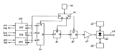
An optical digital-signal-transmitting unit according to the present
invenzion will be now described with reference to Fig. 1.
In a block diagram, an input interface for a given number of electric
signals in a digital form, all of same frequency f1 has been
identified by reference numeral 210. In the figure three digital
signals 201 202, 203 referred to as tributary signals, are shown at
the input of the synchronizing circuits 207, 208, 208 forming the
interface 210 respectively, and in the following of the description
reference will be made to the case in which three tributary signals
PC 664 G 1 71~ 76,1
are transmitted. The device however can be intended for any other
number of independent tributary signals, a person skilled in the art
being capable of executing the necessary adaptations.
The voltage values corresponding to condition "0" and condition "1"
are the same for all tributary signals and preferably are values
dictated by one of the known standards.
The synchronizing circuits 207, 208, 209 perform the function of
synchronizing the tributary signals. The outputs 11, 12, 13 each
reproduce the respective input signal which is such delayed that the
leading edge is in alignment with a common timing signal, consisting
of a square wave at an input frequence fl at the respective terminals
14, 15, 16, and coming from a timing circuit 30.
The timing signal at frequency f1 is also sent (204, 205, 206) to the
unit generating the tributary digital signals 201, 202, 203 so as to
synchronize these units at a common frequency.
As the synchronizing circuits 207, 208, 209, devices available on the
market may be used, such as for example interfaces following CCITT
standard, named Vii, or EIA standard, named RS 422, in the version
providing counter-directional timing to signals.
The synchronized digital signals from the input interface 210 are sent
to the input ports 21, 22, 23 of a multiplexer 20.
By multiplexer it is intended a digital circuit capable of accepting a
certain number of digital input signals and combining them to form a
single signal to be identified as aggregate signal, of frequency f2,
which is a multiple of fl, containing all information relating to the
input signals in addition to synchronism information sufficient to
enable signals to be separated again from each other.
Multiplexer 20 used in the device of the present invention is such
made as to combine the input signals from terminals 21, 22, 23
2172761
PC 664 12
according to a fixed temporal configuration, referred to as frame, to
form an aggregate signal at a frequency f2, which is the frequency of
a synchronizing signal consisting of an input square wave to terminal
24 coming from terminal 32 of the timing circuit 30.
Frequency f2 is selected such as to verify the relation:
f2 = (n + m) * f1,
wherein n is the number of input signals to multiplexer 20,
corresponding to the number of tributary signals, and m is an integer
greater than zero, linked to the density of synchronism present in the
frame with respect to the combined signals.
The multiplexer temporally divides each of the n input signals into n
words of a given number p of bits and copies each bit of each word at
a given position of a word.of p'(n+m) bits, called aggregate word.
In the aggregate word m words of p synchronism bits are inserted,
which are necessary to reconstruct the position of the bits
corresponding to the different tributary signals, during the receiving
step. The aggregate word is then serially transmitted at a frequency
f2 to the output terminal 25 of the multiplexer. This process of
multiplexing the words of the input signals into aggregate words is
repeated cyclically, so as to achieve an aggregate digital signal of
frequency f2 from terminal 25. The time necessary to the transmission
of one bit of the aggregate digital signal, that is the reversal of
frequency f2, is referred to as symbol interval.
In a device made by the Applicant n = 3 tributary channels were
combined and a value m = 1 was selected. Then f2 = 4' f1 was
selected. The number of bits of each word was fixed to p = 8.
The frame used in the device, such determined as to simplify the
subsequent decoding process, is shown in Fig. 2.
In said frame, the corresponding bits of words of the three input
signals were denoted by AO...A7, BO...B7, CO...C7 and the bits of the
synchronism word by SO...S7.
2172761
Pc 664 13
Said frame can be easily extended to the case of a number of signals
to be combined different from three.
The aggregate output signal from terminal 25 of multiplexer 20 is sent
to a terminal 37 of a differential coding circuit 36 also receiving a
synchronizing input signal at a frequency f2, from terminal 33 of the
timing circuit 30.
The differential coding circuit 36, starting from the aggregate signal
generates a coded digital signal of same frequency which changes its
logic level (that is involves a bit of logic level opposite to the
preceding bit) for each bit at a logic level "1" of the aggregate
signal and stays at the same logic level (that is involves a bit of
same value as the preceding bit) for each "0" of the aggregate signal.
This coded digital signal comes out of terminal 39 of circuit 36.
The differential coding circuit 36 can be made by a T-type flip-flop.
The timing circuit 30 also generates, in addition to the already
mentioned timing signals, a timing signal consisting of a square wave
at a frequency
f3=q f2,
wherein q is an integer greater than or equal to 2. Preferably q Z 4.
In a device made by the Applicant q was selected equal to 16. This
signal is made available at terminal 34.
All timing signals are generated in the timing circuit 30 starting
from a signal at a frequency 2' f3 generated by an oscillator 35.
A modulation circuit 40, made following known techniques, receives at
the input port 41, the coded signal from terminal 39 of the coding
circuit 36 and therewith modulates the phase of the timing signal at
frequency f3, entering the input port 42. The phase-modulated signal
is emitted from terminal 43 of the modulation circuit 40.
The ratio value q between frequencies f3 and f2 establishes the
2172761
~.. Pc 664 14
redundancy degree introduced into the signal by the modulation.
The phase-modulated signal corresponds to a succession of square wave
portions at frequency f3, each comprising q periods of the square
wave, the phase of each portion varying at each bit "1" of the
aggregate signal and staying unchanged at each "0" of the aggregate
signal.
This modulation technique, currently referred to as DPSK (Differential
Phase Shift Keying), is conventionally used for transmission of
digital signals through modems operating on telephone lines of the
traditional type or for transmission via satellites.
The multiplexer 20, differential coding circuit 36 and modulation
circuit 40 can consist of a singleprogrammable logic component, model
XC3030 for example, produced by XILINX Inc., 2100 Logic Drive, San
Jose, CA (US).
The phase-modulated signal is used for modulating the emission
intensity of a coherent-radiation source 46, a semiconductor laser for
example, thraugh a piloting circuit 45 made following a known
technique, which generates the necessary current levels to bring the
laser to an emission condition or under-threshold condition at logic
levels "1" or "0" of the phase-modulated signal.
The radiation emitted from the laser is coupled with an optical fibre
49.
The coherent-radiation source 46 may consist of a semiconductor laser
having an emission in the band at about 1300 nm, of GaInAsP for
example, such as model QLM-3S-86 1-002, produced by LASERTRON Inc., 37
North Avenue, Burlington, MA (US).
This model comprising a Peltier cell for cooling the laser, a
thermistor for temperature measurement and a photodiode for monitoring
the output power, is characterized by an emission wavelength included
2172761
Pc 664 15
between 1290 and 1330 nm and a maximum output power of 2.5 nW.
The optical transmission unit also comprises a circuit 47 for
automatic control of the output power of laser 46 and a device 48 for
automatic control of the temperature thereof, which circuit and device
can optionally make use of power or temperature sensors integrated
into the laser container, as in the case of the cited model.
In a device made by the Applicant, the power control circuit 47 has
been set so that the optical power sent along an optical fibre line
connected to the laser by fibre 49 and a fused-fibre dichroic couper
is about 0 dBm. The laser temperature has been kept at about 25 C by
means of circuit 48.
An optical unit for reception of digital signals according to the
present invention, adapted to receive and decode the signals
transmitted by the disclosed transmitting unit will be now described
with reference to Figs. 3 and 4.
In particular, shown in Fig. 3 is the first section of the optical
receiving unit comprising parts for detection of the optical signal,
amplification and demodulation of same.
In a block diagram, an optical detector identified by reference
numeral 60 consists of a photodiode 50 and a pre-amplifier 51,
preferably integrated with the photodiode, adapted ;to detect an
optical signal at a given wavelength, at the input of an optical fibre
59 coupled with the photodiode, and convert it to an electric signal,
carrying out a first amplification of said electric signal.
The photodiode 50 and pre-amplifier 51 can consist of a PIN - FET
detector with FET of GaAs, model QDFBO10 - 001 for example, available
from the already mentioned LASERTRON. This detector is comprised of a
PIN-type photodiode integrated on a common substrate with a FET of
GaAs used as the pre-amplifier.
2172761
Pc 664 16
Its nominal sensitivity can reach - 50 dBm, although worse values are
not excluded in commercially available products. The nominal
sensitivity is calculated as the optical input power necessary to keep
the BER lower than 10-9 in case of a transmission in a baseband,
wherein by error rate or BER it is intended the probability to receive
an erroneous bit during communication.
The Applicant has noted that it is possible to use a PIN - FET
detector in the device, with FET of GaAs (the reception noise being in
inverse ratio to the frequency and therefore high at low frequencies),
in place for example of a detector with FET of silica (the lower noise
of which is known, although it is of difficult availability on the
market), by virtue of the employed modulation technique moving
transmission from the low-frequency band of the aggregate digital
signal to the carrier band approximately centered at frequency f3, and
by virtue of the introduced redundancy by selecting a frequency f3
which is a multiple of frequency f2. In the carrier band the detector
noise is sufficiently reduced to enable detection, with a reduced BER,
of optical signals having a power lower than the nominal sensitivity
of the detector. Due to redundancy, the aggregate digital signal can
be reconstructed at a frequency f2 even in the presence of residual
noise for the digital signal at a frequency f3, and therefore a
reception with a sufficiently reduced BER can be achieved even in the
presence of an optical power at a reception lower than the detector
sensitivity.
In case of use of detectors of best sensitivity, therefore, the
invention enables the use of transmission lines having a greater
attenuation (longer lines for example, or lines of different
transmission wavelength) or laser sources of lower power.
Block 61 in Fig. 3 represents an amplification and
conversion-to-digital-form stage. It comprises a band-pass filter, a
high-gain amplifier, a threshold circuit and an automatic gain control
circuit.
2172761
PC 664 17
Denoted by 52 is a band-pass filter adapted to remove the noise at
frequencies different from the carrier modulation band, with a
passband centered at frequency f3 of the transmission unit and wider
than the carrier modulation band imparted in the transmission unit.
The passband width of filter 52 can be selected in the order of
4 = f2.
A high-gain amplifier 53, associated with an automatic gain-control
circuit 55 therefore amplifies the filtered signal at a sufficient
voltage level for conversion to digital form. A threshold circuit 54
operates this conversion, generating a logic level "1" each time the
amplified signal exceeds a predetermined threshold and a level "0"
under said threshold.
The band-pass filter 52, high-gain amplifier 53, threshold circuit 54
and automatic gain-control circuit 55 are of the conventional type and
can be made following known circuit techniques, in particular by
application of the necessary measures to avoid in the circuits,
coupling of electric noise from the surrounding environment and other
circuits located in the neighbourhood, in particular the circuits of
the transmission unit in the case in which a transmitting unit and a
receiving unit are made on a single printed circuit to form a line
terminal, as explained in the following.
The requested gain for amplifier 5.3 is linked to the gain of the
optical detector employed. In case of use of the detector of the cited
model, the overall gain of pre-amplifier 51, filter 52 and'amplifier
53 must be close to or higher than 100 dB. The signal amplified and
put to digital form is then sent to the demodulation stage, identified
by 62 in the block diagram of Fig. 3.
This stage comprises a timing-reconstruction circuit, a synchronizing
circuit and a circuit for differential phase demodulation.
The timing-reconstruction circuit 56 generates a timing signal 63
PC664 21l28 61
consisting of a square wave at frequency 2' f3, the phase of which is
periodically locked to the digital signal phase from the amplification
stage 61.
As the timing-reconstruction circuit 56, a phase locked loop (known as
PLL) can be used.
The digital signal from the amplification stage is sampled in a
synchronous manner with this timing signal 63, by a sampling circuit
57.
The sampling circuit 57 can be made by a flip-flop of type D.
Denoted by 58 is a circuit for a differential phase demodulation
receiving at the input, the sampled signal in a digital form from the
sampling circuit 57, and the timing signal 63 at frequency 2' f3 from
the timing-reconstruction circuit 56. Circuit 58 serially processes
the sampled-signal bits, comparing them with a version of same delayed
by a symbol interval (that is 2' q bit) and providing a logic signal
"1" at the output in case of bit variation, and a logic signal "0" in
case of bit permanency. The output signal from circuit a 58 for
differential phase demodulation is indicated as digital signal
received 64.
Circuit 58 can be made by a shift register controlled by the timing
signal 63, acting as a delay line, a gate of XOR function.;'The shift
register contains 2' q bits, that is the number of bits corresponding
to a symbol interval of the aggregate digital signal. The sampled
signal in a digital form from the sampling circuit 57 is
simultaneously sent to the shift register input port and to one of the
input ports of a gate XOR. The gate carries out comparison of the
signal with the version of same signal delayed by a symbol interval
and coming from the output of the shift register. In case of
difference between the two inputs of gate XOR, that is in case of
variation of one of the bits of the synchronized digital signal with
respect to the preceding bit by a symbol interval, there is a logic
PC 664 Z 17 27 61
signal "1" at the gate output, whereas there is a logic signal "0" in
case of likeness between the signals entering the gate, that is in
case of permanency in the logic value of bits located at a
symbol-interval distance.
The gate XOR therefore causes one "1" to correspond to each variation
and one "0" to correspond to each permanency, according to the
reciprocal diagram of the diagram used for differential coding in the
transmitting unit.
By utilizing the differential coding/decoding technique of the
aggregate digital signal in the transmitting/receiving unit, the
receiver structure is greatly simplified as compared with the
traditional art in which reconstruction of the absolute phase of the
signal is provided and the presence of local oscillators having a very
stable phase is required.
Shown in Fig. 4 is a block diagram representing the second section of
the optical receiving unit according to the present invention. This
section is comprised of a digital phase-locked loop, a decision loop,
a demultiplexing stage of the tributary signals and an output unit.
If no noise should be present during transmission, the received
digital signal 64 at the output port of the first section of the
receiving unit should be a signal of frequency f2 reproducing.the
aggregate digital signal present in the transmitting unit.
At the input port of the receiver there is, instead, a high noise, due
in particular to the high attenuation of the optical signals along the
optical fibre line employed for transmission, which reduces the
optical signal power at the detector input to a lower level than the
nominal sensitivity of said detector.
Due to noise, the received signal 64 has a spurious signal at
frequency f3 overlapped with the aggregate signal at frequency f2.
2 ~ ~Z76 1
PC 664 20
Since during the transmission phase the aggregate signal has been made
redundant by modulation at a frequency multiple by a factor q, that is
using q bits for transmission of a bit of the aggregate signal, the
Applicant has noted that it is possible to reconstruct the aggregate
digital signal if the received digital signal 64 is processed so as to
find the digital signal at frequency f2 having the maximum overlapping
with the received signal.
In particular, it has been noted that this processing can be made in
two phases:
- reconstruction of the timing signal at frequency f2 showing the
maximum overlapping with the received digital signal;
- based on the logic values of the 2' q bits of the received digital
signal 64 during a reconstructed symbol interval (that is during a
period of the reconstructed timing signal at frequency f2),
determination of the logic value present the greatest number of times
during that interval.
The logic value thus reconstructed corresponds to the most likely
logic value of the aggregate digital signal during that interval.
The process comprising these two steps can be carried out directly in
a sequential electronic circuit.
Phase-reconstruction of the timing signal at frequency f2 having the
maximum overlapping with the received digital signal is obtained by a
digital phase-locked loop 70 receiving the timing signal 63 at a
frequency 2' f3 at the input port 71 and the received digital signal
64 at the input port 72, and generating the timing signal 74 at
frequency f2, made available at the output port 73.
The phase-locked loop 70 can be made, according to the diagram of Fig.
5, by a frequency-division circuit 65 and a phase-comparison circuit
75.
The frequency-division circuit 65 receives the timing signal 63 at a
~172T6r
Pc 664 21
frequency 2' f3 at the input port 171, carries out a frequency
division according to a factor 2' q and sends a timing signal 74 at
frequency f2 to the output 173. The timing signal 74 transmitted to
the input port 174 of the phase comparator 75, is compared in circuit
75 with the received digital signal 64. If the phases of the two
signals do not show the greatest overlapping, the circuit 75 emits
from output 175 or 176, a signal towards the input 177 or 178 of the
divider 65, in order to delay or advance the phase of the timing
signal 74, respectively.
The phase-comparator circuit 75 comprises a counter of the up/down
type. The counter receives counting pulses from the leading edges of
the received digital signal 64. If the timing signal 74 at frequency
f2, at the terminal input 174 shows a logic level "1", the counter
increases by one unit the counted total amount at each leading edge of
the received signal 64; reciprocally, if the timing signal at
frequency f2 inputted to the terminal 174 shows a logic level "0", the
counter decreases by one unit the counted total amount at each leading
edge of the received signal 64.
Counting of the up/down counter is disabled when the leading edge of
the received signal 64 is at the leading edge of the timing signal 74.
In this manner it is counted the number of times in which, during each
half cycle of the square wave 74, there are bits of the digital signal
64 of a logic level different from that of the square wave 74 and the
difference between the two sums is made. Statistically the two sums
are expected to be the same, because the erroneous bits must be
distributed evenly in time. The counted sum therefore does not greatly
diverge from zero, even in the presence of erroneous bits, in the case
of a "locked" phase, and the threshold of tq is not exceeded. If the
phase of the timing signal 74 is different from that assigned to the
received signal 64, on the contrary, the leading edge of the received
signal 64 is not excluded from counting, as it is no longer at the
leading edge of the timing signal 74; the up/down counter counts the
leading edge of the received signal 64 among the erroneous bits and,
, = 217.,M I 6'#
Pc 664 22
after a certain number of periods of the timing signal 74, the
threshold of tq is exceeded in one of the two counting directions and
a threshold-exceeding signal is generated.
Simultaneously the up/down counter is set to zero.
If exceeding of the threshold takes place in the negative-counting
direction, a signal is sent from the output port 175 of circuit 75 to
the input port 177 of circuit 65, which signal disables counting of
the divider circuit 65 for a period of the timing signal 63 and
therefore delays the phase of the timing signal 75 by the same period.
If exceeding of the threshold takes place in the positive-counting
direction, a signal is sent from the output port 176 of circuit 75 to
the input port 178 of circuit 65, which signal activates a two-unit
counting by the divider circuit 65 during a single period of the
timing signal 63 and therefore advances the phase of the timing signal
74 by the same period.
After a certain number of initial cycles therefore, the timing signal
74 locks the phase of the received digital signal 64, even if the
latter suffers from noise.
Determination of the logic value which is present the greatest number
of times within each reconstructed-symbol interval is made by a
decision circuit, denoted by 80 in the diagram of Fig. 4. This circuit
receives the received digital signal 64 at the input port 81, the
timing signal 74 at frequency f2 at the input port 82, the timing
signal 63 at frequency 2' f3 at the input port 83 and emits the
reconstructed aggregate digital signal at the output port 84.
Circuit 80 can consist of a counter which is set to zero at the
beginning of each symbol interval, that is at each leading edge of the
timing signal 74. This counter counts bit occurrences at a logic level
"1" in the received digital signal 64 at each period of the timing
signal 63. If counting exceeds the q value corresponding to half the
2172761
Pc 664 23
periods of the timing signal 63 during a given symbol interval, the
logic value of the reconstructed aggregate signal emitted from the
output port 84 is put to "1" for that symbol interval. If the
threshold of q countings is not exceeded, a logic value of "0" is
assigned to the reconstructed aggregate signal for that symbol
interval.
The reconstructed aggregate signal according to this technique is the
signal which is most likely to reproduce the aggregate digital signal
present in the transmitting unit.
The multiplexing stage of the tributary signals 90, accomplished by
known techniques, divides the reconstructed aggregate signal entering
terminal 91 into n tributary signals. This stage involves: a
frame-synchronization circuit capable of finding the synchronization
word within the data flow of the reconstructed aggregate signal; a
reconstruction circuit for reconstruction of the timing signals at
frequency f1 relating to each of the tributary channels starting from
the timing signal 74 entering the terminal 92, by division of signal
74 and alignment based on the frame structure; and a demultiplexer
capable of recognizing, within the frame structure, the bits
corresponding to the various tributary channels and separating them
towards the output ports.
The frame synchronizing circuit can be made by a finite-state machine.
The ~timing-signal reconstruction circuit can be formed of an n-d.ivider
controlled by the frame synchronization circuit.
The demultiplexer can be made of a programmable logic component, model
XC3030 for example, available from the already mentioned XILINX.
The outputs from the tributary digital signals (93, 94, 95 in the
figure referring to the case of n = 3 tributary signals) and the
respective timing signals at frequency f1 (96, 97, 98) are sent to the
input ports 111, 112, 113 and 114, 115, 116 respectively of an
2172761
PC 664 24
interface 100 made up of circuits 107, 108, 109.
As the circuits 107, 108, 109, devices available on the market may be
used, such as for example interfaces constructed following the already
mentioned standards V11 or RS 422, in the version providing a
co-directional timer to the signals.
The outputs from the interface 100 contain the tributary signals 101,
102, 103 and related timing signals 104, 105, 106.
A receiving unit and a transmitting unit of the type described can be
disposed to form a line terminal adapted for use as receiving and
transmitting station along an optical transmission line. Referring to
Fig. 6 reproducing a diagram of this line terminal, the first and
second sections of an optical receiving unit according to the present
invention, made as described with reference to Figs. 3 and 4, have
been denoted by 120 and 130. The reconstructed tributary signals (101,
102, 103 in the case n = 3 as provided in the figure) are sent both to
the output ports and the change-over switches (141, 142, 143). Through
the change-over switches the input signals to the transmitting unit
150 (made as described with reference to Fig. 1 and the timing signals
of which 161, 162 are directly picked up from units 120, 130) can be
selected from signals 101, 102, 103 coming from the receiving unit and
a series of independent tributary signals 201, 202, 203. In this
manner the "stepping-over" function controlled from the outside can be
accomplised, according to the "Data Terminal Ready" modalites provided
by standard ISO' 2110, to which data interfaces refer: this means that
the terminal can be controlled so as to operate as a repeater towards
fibre 49 of the optical signals received from fibre 59, or as a
receiver of the optical signals from fibre 59 and transmitter to fibre
49 of the locally-generated digital signals 201, 202, 203.
The described line terminal can be used for amplification and
regeneration of optical signals along a high-attenuation optical
communication line.
2172761
~-- PC 664 25
In particular, it can be employed for bidirectional transmission of
service signals along an optical-fibre communication line, according
to the general diagram shown in the above mentioned US Patent
5,113,459.
An optical telecommunication system according to the present invention
is depicted in Fig. 7. In said system the bidirectional transmission
of service signals is provided, over a channel of a wavelength
different from that of the communication signals, along the same
optical fibre-communication line 3 employed for transmission of the
communication channels.
As shown in the figure, a telecommunication line of the optical type
generally comprises one station 1 for emitting optical signals in
which the signals 2 to be transmitted are received usually in the form
of electric signals and emitted in an optical form through an optical
fibre 3 forming the line.
At the opposite end of fibre 3, at a great distance (even some hundred
kilometers) from the emission station 1, there is a receiving station
4 adapted to receive the optical signals transmitted along the fibre,
to convert them to signals of another nature, electric signals for
example, and send these signals 5 to the use apparatus, not shown.
As shown in Fig. 7, at each optical amplifier 8 of the active-fibre
type with fluorescent dopant for example, two dichroic couplers 9 are
present upstream and downstream of said amplifier, said couplers being
adapted to receive at a common input port, the communication signals
and service signals having different wavelengths and multiplexed on
the same fibre, and to separate at the output on two outgoing fibres
9a and 9b, the communication signals at one wavelenth and the service
signals at a different wavelength respectively, and also adapted to
send to a single outgoing fibre, the communication signals and service
signals separately inputted to fibres 9a, 9b.
Similar dichroic couplers are present at the emitting and receiving
2172761
'-- PC 664 26
stations 1, 4.
Conveniently, the wavelength of the service signals is selected so as
to be greatly different from the communication one; under this
condition, the dichroic couplers ensure an optimal separation between
the signals.
The communication wavelength is usually included between 1500 and 1600
nm, in a region named "third window", in order to operate at a minimum
of the light attenuation within silica glass fibres, as
diagrammatically shown in Fig. 6; this, as requested for
telecommunications, enables data transmission at high speed, in the
order of some hundred Mbit/s, over distances of some ten or hundred
kilometers before the amplification, keeping the signals to
sufficiently high levels for a correct final reception.
The service signals, on the contrary, due to their features, can be
transmitted at low-speed, in the order of some hundred Kbit/s, in
particular at a speed lower than 300 Kbit/s; according to the present
invention these service signals are conveniently generated at a
wavelength included in a range centered on 1300 nm, at a secondary
minimum of the light attenuation curve in the silica glass, named
"second window". The width of this range depends on the specific
features of the line fibre used; a preferred range for line fibres of
usual production can be of 1200 to 1400 nm.
Each dichroic coupler 9 is connected, together with the respective
output fibre 9b carrying the service signals, to a respective
connecting unit 10, through which the optical service signals from the
coupler are received and converted to corresponding electric output
signals, and electric input signals are converted to optical signals
at the service wavelength and admitted to the fibre 9b entrance to be
multiplexed along the line. This unit can be formed of a line terminal
of the type described with reference to Fig. 6. The use of two line
terminals 10 at each optical amplifier 8 enables a bidirectional
service signal transmission along the optical communication line 3.
2172761
Pc 664 27
In this manner, an optical signal, at 1300 nm, extracted from the line
3 of the dichroic coupler 9 is converted to a corresponding electric
signal which can be employed for the intended uses, such as for
example service telephone communications by the maintenance staff or
control of the optical amplifier 8, as shown in phantom lines in Fig.
7, or for other commands or controls; likewise, electric control
signals or service telephone communications can be thrown into the
fibre 3 of the line to reach other destinations.
In order to enable the service signal to reach amplifiers or end
stations located to a great distance from the signal-emitting site,
along a fibre having several optical amplifiers, the electric signal
coming out of a unit 10 connected to a dichroic coupler 9, located
upstream of an optical line amplifier 8 can be sent, via a change-over
switch 141, to the input port of a unit 10 connected to a second
dichroic coupler 9 downstream of the optical amplifier, adapted to
send the suitably amplified service signal along the subsequent
optical fibre portion, until the arrival station or a new optical
amplifier.
In this manner the service signal is amplified in a self-contained
manner at each optical amplifier of the line and can therefore cover
the whole requested distance reaching its destination at a sufficient
level for the intended purposes.
Experiment
The Applicant has made and experimented ailine terminal of the same
type as described with reference to Fig. 6, in which the transmitting
and receiving units have been made following the preceding
descriptions, using the components and parameter values previously
pointed out as the preferential ones and having the following values
for the frequencies of the timing signals:
f1 = 64 KHz
f2 = 256 KHz
f3 = 4096 KHz.
2d 7~ 761
Pc 664 ~
For submitting the device to the experiment, an optical connection
simulating the conditions along a high-attenuation optical-fibre line
was utilized. This connection is shown in Fig. 8.
Two line terminals according to the invention have been denoted by 200
and 300 and they comprise respective transmitting units (250, 350),
change-over switches (240, 340) and receiving units consisting of a
first section (220, 320) and a second section (230, 330).
In order to generate the digital test signals at a frequency of 64
Kbit/s to be inputted to the transmitting unit 250, analyze the data
from the receiver 220 - 230 . and measure the BER, a data
generator/analyzer 151, model MD6420A produced by ANRITSU Corp.,
5-10-27 Minato-ku, Tokyo (JP) was used.
The optical signals at the wavelength of about 1300 nm produced by the
transmitting unit 250 were sent along a single-mode optical fibre 152
to the receiving unit 320 of the line terminal 300. A variable optical
attenuator 153, model MN939C, of the above mentioned ANRITSU was
placed along the fibre 152.
The terminal 300 was made up in the repeater mode connecting the input
ports of the transmitting unit 350 to the output ports of unit 330.
The optical signals generated by the transmitting unit 350 were sent
to the receiving unit of the line terminal 200 by a single-mode
optical fibre 152 and a variable attenuator 153, both like those
already described.
To ensure symmetry of the transmission condition in the two ways,
adjustment of the two variable attenuators was always carried out so
as to give the same attenuation coefficient.
The analog signal present at the amplifier output of the receiving
unit 220 was detected by an oscilloscope model TDS320 available from
TEKTRONIX S.p.A., via Lampedusa 13, Milan (IT).
2172761
Pc 664 29
Fig. 9 shows the eye diagram measured in the case in which the
variable optical attenuators 153 had been adjusted so that the
received optical power was -50 dBm.
The eye diagram is shown open, to denote an optimal transmission
quality. In confirmation of that, no transmission errors were detected
during the period of observation of 14 hours.
Then transmission tests were executed by varying adjustment of the
variable attenuators so that the optical power would take values from
-56 dBm to -61 dBm, with steps of -1 dBm. The eye diagrams detected at
the receiver are reproduced in Figs. l0a - lOf.
It is possible to see that the eye diagram is well open in the case of
optical power at the receiver of -56 dBm and progressively closes on
decreasing of the optical powers, until it becomes completely closed
for an optical power of -61 dBm at the receiver.
Simultaneously, the BER value for each of the optical powers was
measured.
Fig. 11 reproduces the graph resulting from these measurements, with
the BER value reproduced in a logarithmic scale on the y-axis,
depending on the optical power at the receiver on the x-axis.
It is possible to see that the BER is lower than 10-5 for optical
powers at the receiver greater than -60 dBm. The value of 10-5 is the
typical BER value for telephone communication lines (see, the text
"Telecommunication networks: protocols, modeling and analysis" by M.
Schwartz, Addison-Wesley, 1987, in particular page 134, for example),
and it is therefore a sufficient value for the transmission of service
communications of the sound type, through a coding of the PCM type
according to laws A or Mu(CCITT) for example, or for data
transmission, through the digital coding protocol HDLC (High-level
Data Link Control) for example. In addition, it is possible to see
that a BER of 10-9 occurs for an optical power at the receiver of only
2172761
~-- Pc 664 30
-56 dBm, lower than the nominal sensitivity of the detector.