Note: Descriptions are shown in the official language in which they were submitted.
CA 02172812 2004-02-24
75721-6
1
METHOD FOR COMBINING A PLURALITY OF INDEPENDENTLY
OPERATING CIRCUITS WITHIN A SINGLE PACKAGE
FIELD OF THE INVENTION:
This invention relates generally to digital circuitry and, in particular, to
methods
of designing and constructing digital circuitry.
BACKGROUND OF THE INVENTION:
An Application Specific Integrated Circuit (ASIC), also referred to as a gate
array,
is a well known device for constructing digital circuitry and, most
particularly,
digital data processing circuitry. An ASIC includes a large number of
uncommitted
logic functions, such as gates and inverters, and assemblages of logic
functions,
such as flip-flops, counters, and memory elements. Based on a schematic
diagram
of a user's circuit, the ASIC circuits are selected and interconnectxd so as
to
realise the desired functions. As a result, a circuit that would require a
large
number of discrete integrated circuit packages to construct can be realized
instead
within a single integrated circuit package. Advantages to this approach
include
considerable reductions in packaging volume, power, and propagation delays
over
a conventional circuit constructed with discrete integrated circuit packages.
One disadvantage to the use of an ASIC is the considerable cost incurred in
evolving the initial design through at Ieast one circuit specificstion and
fabrication
cycle to arnve at a finished and fully functional integrated circuit. A
related
problem is a lack of an ability to make substantive circuit changes to the
completed ASIC to accommodate circuit corrections and design changes.
Typically,
each required revision to the original ASIC design results in additional and
substantial costs being incurred. Also, for many applications the full
capability of
the ASIC is not required, resulting in some number of circuits being unused.
For
2172812
.;o oRSa rcr~~sam.m~4F
2
e~amnle, a given design rr~a~- require an ASIC ha~2ng a minimum of 3001
:nter~face
pins. However, the actual number o:;~ gates or cells that a-re required to
implement.
the design ma5~ be onJ~~ a small fracr,"ion of the total number tha* are.
avaiiabJe for
the ASIC that is selected to meet the interface pin requirements.
As can be appreciated, the foregoing disadvantages are compounded when a
design
requires the use of t~~o or more ASICs. Additionally, the requirement to
schedule
the timel~~ production of, and stock, a number of different ASICs can increase
over<iIl s~~st.em costs. F,arthermore. although a relativel~~ large total
number of
ASlC;s may be pro~~ided to a customer by a given ~~endor, the number for each
of
the different. ASICs ma5l be less than a minimum threshold number reauir ed to
obtai n a significant. volmme discount.
Ref~=rences Dl and D2 both re, late to integrated circuit technology,
wherein D1 relates specifically to providing two designs in one LSI
package, and D2 relates to ASIC technology.
OBJECTS OF THE IN~-rENTIOI~T:
It. i= thus one object. of this invention to pro~-idP a method for speci~,-ing
a rate
a:. ay integrated circuit. tho t overcomes the problems of the prcr art..
It i: another object. of this invention. to provide an integr ated cir cult
tha; includes
a plurality of circuit, blocks, each being independent of the other, and a
gating
mechanism that is responsive to externally excited mode select inputs to
selectively couple one of the circuit blocks to interface pins of the
integrated
cirn.tllt.
SLTMMAR~ OF THE INV~EN'I'ION
The foregoing and other problems are overcome and the objects of the invention
are realir.ed by a method of fabric:at:ing an integrated circuit. The method
includes
th~~ st.eps of: (a) providing at least two circuit designs; (b) determining a
total
number of gates that are required to implement the at least two circuit design
wlithin a gate array; (c~) determini.ng a greatest total number of interface
pins that
are required b~1 one of the designs; ( d ) selecting a gate array type that
has a total
nmmber of gates that exceeds the determined number of gates and that has a
total
nLU~ober of interface pins that; exceeds the determined greatest. total n
umber of
interface pins; (e) translating each of the designs into a gate arz-a~l
equivalent. to
provide a specification of a gate array til-cait block for each of the
designs: (f>
AMENDED SHEET
CA 02172812 2004-02-24
75721-6
3
defining at least one interface pin to be a mode select input pin; and tg)
determining a gate equivalent of a gating logic block for selectively coupling
only
one of the circuit blocks to the interface pins of the gate array in
accordance with
an input signal to be applied to the at least one mode select pin.
Further in accordance with this invention, an integrated circuit having a
plurality
of interface pins includes a first circuit block that is comprised of a
plurality of
gate-equivalent circuits; the first circuit block being a first partition of a
data
processing system. The integrated circuit further includes at least one other
circuit
block comprised of a plurality of gate-equivalent circuits; the at least one
other
circuit block being a second partition of the data processing system. The
circuit
blocks are capable of operating independently of one another, with each
performing an associated function. At least one mode select interface pin is
provided, in conjunction with gating circuitry that is interposed between the
circuit blocks and the interface pins for selectively coupling, in accordance
with a
- logic level applied to the at least one mode select interface pin, only one
of the
circuit blocks to the interface pins.
In accordance with a further aspect of this invention there are at least two
mode
select interface pins. For this case a logic level of a first one of the mode
select
interface pins specifies a circuit block for coupling to the interface pins,
and a logic
level of a second one of the mode select interface pins specifies a mode of
operation
of a specified circuit block.
CA 02172812 2004-02-24
75721-6
3a
According to one aspect of the present invention,
there is provided a method of fabricating an integrated
circuit, comprising the steps of: providing at least two
circuit designs; determining a total number of gates that
are required to implement the at least two circuit designs
within a gate array; determining a maximum number of
interface terminals that are sufficient to accommodate the
interface terminal requirement of the circuit design that
has a largest interface terminal requirement; selecting a
gate array type that has a number of gates that is greater
than the determined number of gates and that has a number of
interface terminals that is sufficient to accommodate the
determined maximum number of interface terminals;
translating each of the designs into a gate array equivalent
to provide a specification of a gate array circuit block for
each of the designs; defining at least one interface
terminal to be a mode select input terminal; and determining
a gate equivalent circuit of a gating logic block for
selectively coupling only one of the circuit blocks to the
interface terminals of the gate array in accordance with a
logic state of an input signal to be applied to the at least
one mode select terminal.
According to another aspect of the present
invention, there is provided an integrated circuit having a
plurality of interface terminals, said integrated circuit
being used in the construction of a data processing system
that includes at least two partitions, each of said at least
two partitions being comprised of circuitry that is
necessary to implement at least one circuit block of the
data processing system, said integrated circuit comprising:
a first circuit block comprised of a plurality of gate-
equivalent circuits, said first circuit block comprising
said first partition of the data processing system; at least
CA 02172812 2004-02-24
75721-6
3b
one other circuit block comprised of a plurality of gate
equivalent circuits, said at least one other circuit block
comprising said second partition of the data processing
system; at least one control interface terminal; and gating
means interposed between said first and second circuit
blocks and said interface terminals for selectively
coupling, in accordance with a logic level applied to said
at least one control interface terminal, only one of said
circuit blocks to said interface terminals, whereby a first
one of the integrated circuits is used at one location on a
circuit board substrate for implementing the circuitry of
the first partition and a second one of the integrated
circuits is used at another location on the circuit board
substrate for implementing the circuitry of the second
partition, in accordance with the logic level applied to
said at least one control interface terminal at said first
and second locations.
According to still another aspect of the present
invention, there is provided an integrated circuit having a
plurality of interface terminals, said integrated circuit
being used in the construction of a data processing system
that includes at least two partitions, each of said at least
two partitions being comprised of circuitry that is
necessary to implement at least one circuit block of the
data processing system, said data processing system further
comprising a central processor (CP), and IO controller
(IOC), and a main memory, said integrated circuit
comprising: a first circuit block comprised of a plurality
of gate-equivalent circuits, said first circuit block
comprising said first partition of the data processing
system, said first partition comprising means for buffering
addresses received from the central processor (CP) and
addresses received from the IO controller (IOC) before
CA 02172812 2004-02-24
75721-6
3c
application of the addresses to the main memory; a second
circuit block comprised of a plurality of gate-equivalent
circuits, said second circuit block comprising said second
partition of the data processing system and including means
for buffering data received from the central processor (CP)
and data received from the IO controller (IOC) before
application of the data to the main memory; at least two
control interface terminals; and gating means interposed
between said first and second circuit blocks and said
interface terminals for selectively coupling in accordance
with logic levels applied to at least one of said at least
two control interface terminals, when installed upon a
printed circuit board, only one of said circuit blocks to
said interface terminals for connecting the selected circuit
block to the CP, to the IOC, and to the main memory, whereby
a first one of the integrated circuits is used at a first
location on the printed circuit board for implementing the
circuitry of the first partition and a second one of the
integrated circuits is used at a second location for
implementing the circuitry of the second partition, in
accordance with the logic level applied to said at least one
of said at least two control interface terminals.
According to yet another aspect of the present
invention, there is provided an integrated circuit having a
plurality of interface terminals, said integrated circuit
comprising: a first circuit block comprised of a plurality
of circuits, said first circuit block comprising a first
partition of a data processing system; at least one other
circuit block comprised of a plurality of circuits, said at
least one other circuit block comprising a second partition
of the data processing system; wherein said first circuit
block and said at least one other circuit block perform
different logical functions of the data processing system;
CA 02172812 2005-O1-14
75721-6
3d
at least one control interface terminal; and gating means
interposed between said first and second circuit blocks and
said plurality of interface terminals for selectively
coupling, in accordance with a logic level applied to said
at least one control interface terminal, only one of said
circuit blocks to said plurality of interface terminals.
According to a further aspect of the present
invention, there is provided a data processing system
comprised of a central processing unit, a memory for storing
data, and a bus for coupling said central processing unit to
said memory, the bus including a plurality of signal lines
for conveying at least memory addresses from said central
processing unit to said memory and for conveying data
bidirectionally between said central processing unit and
said memory, said data processing system further comprising
bus interface circuitry that is interposed within said bus
between said central processing unit and said memory, said
bus interface circuitry comprising address interface
circuitry and data interface circuitry, wherein said address
interface circuitry and said data interface circuitry are
disposed within each of a plurality of integrated circuit
packages having a plurality of interface terminals and at
least one control input terminal, wherein said plurality of
interface terminals and said at least one control terminal
of each of said plurality of said integrated circuit
packages are electrically coupled to circuit wiring of at
least one printed circuit board, wherein said at least one
control terminal of a first one of said plurality of
integrated circuit packages is electrically coupled to a
first logic potential for selecting only said address
interface circuitry to be coupled to said plurality of
interface terminals and, through said plurality of interface
terminals, to circuit wiring that is electrically coupled to
CA 02172812 2004-02-24
75721-6
3e
said address signal lines; and wherein said at least one
control terminal of a second one of said plurality of
integrated circuit packages is electrically coupled to a
second logic potential for selecting only said data
interface circuitry to be coupled to said plurality of
interface terminals and, through said plurality of interface
terminals, to circuit wiring that is electrically coupled to
said data signal lines.
BRIEF DESCRIPTION OF THE DRAWINGS
The above set forth and other features of the
invention are made more apparent in the ensuing Detailed
Description of the Invention when read in conjunction with
the attached Drawings, wherein:
Fig. 1 illustrates the arrangement of Figs. 2A-2D;
Figs. 2A-2D are each a portion of a block diagram
of a data processor that is constructed and operated in
accordance with this invention so as to include a
WO 95/10854 2 i 7 2 812 PCT/US94/03098
4
common gate array package that is used in a plurality of different locations
for
different circuit functions;
Fig. 3 illustrates the arrangement of Figs. 4A-4D;
Figs. 4A-4D are each a portion of a block diagram of a Memory Address Unit
(MAU) that is a component of the block diagram of Figs. 2A-2D, the MAU being
one circuit block that is included within the single integrated circuit of
this
invention;
Fig. 5 illustrates the arrangement of Figs. 6A-6D;
Figs. 6A-6D are each a portion of a block diagram of a Memory Data Unit (MDU)
that is a component of the block diagram of Figs. 2A-2D, two of which are
specifically illustrated in Fig. 2C, the MDU being another circuit block that
is
included within the single integrated circuit of this invention;
FIG. 7 is a block diagram of a gate array that is constructed in accordance
with
this invention; and
FIG. 8 is a flowchart that illustrates a method of this invention.
DETAILED DESCRIPTION OF THE INVENTION
The teaching of this invention is now described in the context of a presently
preferred embodiment thereof. Specifically, the teaching of this invention is
described in the context of a data processor 10 that is illustrated in Figs.
2A-2D.
As will become apparent below, the data processor 10 includes several complex
circuit blocks (CDU, MAU, MDUs~ that are shown and described separately.
However, and in accordance with this invention, these circuit blocks are all
fabricated within a single gate array 300 (FIG. 7). The gate array 300 is
provided
with a plurality of input mode pins that define the functionality that the
gate
array will assume when installed in. the circuit board upon which the data
processor 10 is constructed. At a given circuit board position predetermined
logic
WO 95/10854 ~ pCT/US94/03098
levels are applied to the input :mode pins to selectively set internal gating
so as to
interconnect a desired circuit block to the interface pins of the gate array.
The
other, non-selected circuit blocks are not used.
Before describing the teaching ~of the invention in further detail, reference
is made
to FIGs. 2A-2D for showing a presently preferred embodiment of a data
processing
system that makes use of this invention.
A Central Processor (CP) 12 is coupled to an 8K by 88-bit Control Store 14 by
a
14-bit control store address bus 14a and an 88-bit control store data bus 14b.
The
Control Store 14 stores macroinstructions which are read into the CP 12 in
order
to execute macroinstructions that are read from an 8K by 72-bit CACHE memory
16, via a CACHE Data Unit (CDU) 18, bidirectional 64-bit buffered data store
bus
BDSB00:63 18a, and bidirectional 32-bit data bus DB00:32 12a.
Macroinstructions are fetched from the CACHE memory 16 in accordance with
physical addresses provided b~y the CP 12 on a 32-bit physical address bus
(PA0:31) 12b, via a CACHE address multiplexer (MUX) 20. The CACHE address
MUX 20 is employed when pre-filling the CACHE 16 with instructions and data.
In this embodiment of the invention only PA bits 16:28 are provided to the
CACHE 20. PA bit 28 being provided as the LSB address bit enables a Double-
Word (eight bytes or two 32-bit words) to be read by the CP 12 over the 64-bit
BDSB 18a and 32-bit bus 12a. 'rhe eight bit DSP0:7 bus 18b conveys data parity
bits between the CACHE 16 a~ad the CDU 18. The CDU 18 operates as a data
buffer for interfacing the 32-b:it CP 12 data bus 12a to the 64-bit cache/main
memory BDSB 18a, as a data error checker, and provides data alignment for the
CP 12.
In the illustrated embodiment. the macroinstructions that are read from the
CACHE 16 are those that implement a VS assembly language program that is
provided by Wang Laboratories Inc. of Lowell MA.
WO 95/10854 2 i l 2 B 12 PCT~S94/03098
6
The 32-bit processor data bus 12a is buffered by a transceiver 22 and is
provided
as a buffered data bus (BDB0:31) 22a to several locations, including a 16K by
8-bit
Data Key memory 24, a 16-bit control and status register (XCTLREG) 26, a
reference and change table (REF/CNG TABLE) 28, and a system (backplane) Bus
Interface Chip (BIC) 30. This data path gives the CP 12 an ability to send
control
information to, and read status information from, these various devices.
The Data Key memory 24 stores encrypted information and provides a capability
to enable only specified software packages to be executed by the CP 12. The
REF/CNG Table 28 functions to indicate a reference to a particular page of
memory, and to indicate if the reference was a write operation. The BIC 30
provides an interface to other components that are coupled to the system bus
32,
the system bus including a 32-bit multiplexed address/data bus (AD31:0) 32a,
associated parity lines (PAR3:0) 32b, and control signal lines 32c. In
general, the
BIC 30 operates to arbitrate access to the system bus 32 and to perform all
necessary handshaking with other devices that are coupled to the system bus
32.
The XCTLREG 26 enables control over the CACHE memory 16, indicates CACHE
status, and also provides indications of correctable and uncorrectable data
errors.
A buffer 34 drives the PA bus 12b as a CP Address (CPA) bus 34a to the Data
Key
24 (14 bits), the REF/CNG Table 28 (16 bits) and a Memory Address Unit (MAU)
36 (27 bits). The MAU 36 is shown in greater detail in Figs. 4A-4D. The MAU 36
operates to queue memory read and write addresses and functions, in
conjunction
with even and odd Memory Data Units (MDUs) 38a and 38b, respectively, (Figs.
6A-6D), to write and read data from main memory 40. Main memory 40 is
comprised of a plurality of DRAM modules 40a-40d, and is organized as an even
word array (modules 40a and 40b> and as an odd word array !modules 40c and
40d>. The total width of the main memory 40 is 64 bits to double word), plus
14
bits of parity information. Parity is determined separately on each odd and
even
32-bit memory word.
s
The MAU 36 also receives a 27-bit I/O address (IOA) bus 36a that is sourced
from
WO 95/10854 217 2 812 PCT/US94/03098
7
the BIC 30 via a Buffered Address (BA) bus 30a and a latch 42. IOA bus 36a
provides a first memory address of a data block that is to be written to or
read
from by an UO device that is coupled to the system bus 32. The first address
is
received though a transceiver 44, a buffered address/data (BAD) bus 44a, and a
transceiver 45. Transceiver 45 is enabled to pass the first memory address of
the
memory block to the BIC 30 anal the latch 42, via the BA bus 30a. In the MAU
36
the first address is buffered, and subsequent memory addresses are incremented
by the BIC 30 during an I/O operation and provided over the buses 30a and 36a,
via latch 42. This enables a potentially large number of reads or writes to be
made
to consecutive memory locations of the main memory 40. The operation of the
MAU 36 will be described below in greater detail.
One output of the MAU 36 is a 22-bit memory address (MA) bus 36b that is
applied to a row/column MUD. 46 which has a 12-bit output for sequentially
providing row and column addresses, via drivers 48a-48d, to the DRAM modules
40a-40d, respectively. The row/column MUX 46 operates under the control of a
COL signal that is generated by a memory control state machine that forms a
part
of a memory controller 31.
Another output of the MAU 36 is a 24-bit update address (UPDT) bus 36c that is
latched by a register XMAR 50. XMAR 50 sources a registered update address
(RUPDT) bus 50a to the MUX :Z0 (13 bits), to a MUX 52 (24 bits), to a driver
54,
and to an External Tag Store SEi. Also provided to MUX 52 is the PA bus 12b.
The
output of the MUX 52 is a 13-bit internal tag store address (ITSA) bus 52a and
an 11-bit internal tag store data (ITSD) bus 52b which are applied to an
Internal
Tag Store 58. The output of the driver 54 is a 13-bit external tag store
address
(XTSA) bus 54a which is applied to the External Tag Store 5F. i..n conjunction
with
11-bits of the RUPDT bus 50a. The External Tag Store 56 and the Internal Tag
Store 58 provide CACHE hit and miss detection, XMIS and IMIS, respectively,
for
I/O accesses and CP 12 accesses, respectively.
s
The MDUs 38a and 38b operate in conjunction with registered buffers 60a and
WO 95!10854 217 2 812 pCT~S94/03098
8
60b, respectively, to provide a data queue for read and write accesses of the
main
memory 40. The MDUs 38a and 38b also each provide for word-wide ECC
generation and checking functions for data going to and coming from the main
memory 40. Each of the MDUs 38a and 38b is bidirectionally coupled to one word
(32-bits) of the 64-bit buffered data store bus 18a, and thereby to the CACHE
16
and to the CDU 18. Each of the MDUs 38a and 38b also source 4-bits of the 8-
bit
CP Data Parity (CPDP) bus which is provided through a buffer 64 to the eight
bit
DSP0:7 bus 18b that conveys data parity bits between the CACHE 16 and the
CDU 18. The MDUs 38a and 38b each also have a 32-bit I/O data path (IOD) and
are bidirectionally coupled in parallel to a transceiver 62 and thence to the
BAD
bus 44a. For I/O data transfers to or from the system bus 32 the MDUs are
alternately selected to either transmit up to a 32-bit word to the transceiver
62,
or receive up to a 32-bit word from the transceiver 62. The MDUs 38a and 38b
are
described below in greater detail.
The above-mentioned memory controller 31 (FIG. 2D) includes a memory request
arbitration state machine that is responsive to CP memory requests, IO memory
requests, and Refresh memory requests. The memory controller 31 also includes
a DRAM control state machine. The memory controller 31 operates to control
access to, and the sequencing of, the main memory 40. The timing signals that
are
generated by the memory controller 31 provide for quad-word read, CP write,
word/double-word write, and partial or read-modify-write (RMW) operations,
respectively.
The data processor 10 of Figs. 2A-2D, in a presently preferred embodiment of
the
invention, is packaged on a single mufti-layered printed circuit board. In
accordance with this invention, the CDU !g. MAU 36, and the MDUs 38a and 38b
are each contained within a single ASIC or gate array package that is used at
a
plurality of different circuit board positions.
Reference is now made to Figs. 4A-41~ which illustrate the construction of the
MAU 36 that is shown in Fig. 2A. A CP/IO Write Register Control 70 receives as
WO 95/10854 21 l 2 ~ 12
PCT/US94/03098
9
inputs a 3-bit CP command (CPCMD) 70a, a 3-bit IO command (IOCMD) 70b, the
three LSBs of the CP address (CPADR) bus 34a, and the three LSBs of the IO
address (IOADR) bus 36a. Bae~ed on this information the Write Register Control
70 provides a first 5-bit code (CPLD) 70c that specifies to the MDUs 38a and
38b
a CP 12 data modifier field, and a second 5-bit code (IOLD) 70d that specifies
to
the MDUs 38a and 38b an IO data modifier field. As such, CPLD and IOLD are
employed during write operations, as described below, to cause the loading
into the
MDU 38 of a designated byte or bytes, and to set Mark bits accordingly.
The MAU 36 also includes an Address Register clock enable block 72 that
receives
two CP 12 clock signals (CKCF') 72d and which outputs clocks 72a, 72b, and 72c
to a first CP Address Register (CP ADDR REGO) 74, a second CP Address Register
(CP ADDR REG1) 76, and a CAP Previous Address Register 78, respectively.
For a first CP 12 memory write operation 24-bits (05:28) of the associated
memory
address are latched from the C'PADR bus 34a into the CP ADDR REGO 74, and
also into the CP Previous Address Register 78, and a CP Memory Request
(CPMREQ) is asserted to the memory controller 31 of FIG. 2D. The MAU 36 stays
in this condition if another CP write does not occur (CPWR*), and so long as
the
requested CP memory write opE~ration does not complete (CMPL*). If the memory
operation is not completed (CMPL*) before a next CP 12 memory access (CPWR),
then 24-bits of the next memory address are latched into the CP ADDR REG1 76
(CKCP1), and also into the CP :Previous Address RegYSter 78. It is noted that
the
CP Previous Address Register 'T8 is clocked whenever CP ADDR REGO 74 or CP
ADDR REG1 76 is clocked to si;ore the CP write address that is being received.
Subsequently another CP memory request is issued to the mamory controller 31
(CPMRE(a), and the MAU 36 remains in the same state until the memory request
for the first CP write operation completes ( CMPL). While in this state CP
ADDR
REG1 76 is clocked (CKCPl) on the occurrence of another CP write, and if a
comparator 80 indicates a match (CPAMTCH 80a) between the CP write address
being received and the CP writ,e address that is stored in the CP PREV ADDR
WO 95/10854 Z ~ i 2 312 PCT/US94J03098
REG 78, and if the previously requested memory operation has not completed.
That is, CKCP1 = CPWR and CPAMTCH and CMPL*. The assertion of
CPAMTCH 80a indicates that the current CP write operation is directed to the
same double word of memory as the previous CP write operation whose address
is stored in CP ADDR REG1 76. The CPAMTCH signal 80a is used to initiate a
selective combination of the current write data with registered write data
from one
or more previous and yet unexecuted CP write operations. The specifics of the
MDU 38 write merge operation are described below.
In this state, and if a CP write is received that does not generate a match
with the
content of the CP PREV ADD REG 78 (CPAMTCH*), then a write stop (WRSTCP>
signal is asserted to halt the CP write operation. This is accomplished in
response
to the occurence of two buffered CP write operations, and the generation of a
third
that is not directed to the same double word as the last CP write operation
whose
address is buffered in CP ADDR REG 1 76.
When the first requested CP write operation (associated with the address
stored
in CP ADDR REGO 74) completes (CMPL) the CP write stop signal is removed.
The state machine stays in this state so long as there is not another CP write
(CPWR*), and there is no completion of the second CP memory request that was
issued for the address stored within CP ADDR REG1 76. If another CP write
operation does occur (CPWR), and if the memory write operation also completes
(CMPL), then the CP ADDR REGO 74 is clocked (CKCPO) to store the current
write address. The assertion of CKCPO also causes the CP write address to be
stored within the CP PREV ADDR REG 78. If, however, another CP write
operation occurs (CPWR) before the memory write operation completes (CMPL* ),
then the CP ADDR REGO 74 is clocked t CKCPO ~ to store the associated write
address. As before, the assertion of CKCPO also causes the CP wxite address to
be
stored within the CP PREV ADDR REG 7 8.
Subsequently, a CP memory request (CPMREQ) is issued to the memory controller
31, and the MAU 36 remains in the same state until the memory request for the
second CP write operation completes ( CMPL). While in this state the CP ADDR
WO 95/10854 21 l 2 812
PCT/US94/03098
11
REGO 74 is clocked (CKCPO) on the occurence of another CP write, and if the
comparator 80 indicates a match (CPAMTCH) between the CP write address being
received and the CP write address that is stored in the CP PREV ADDR REG 78,
and if the previously requested memory operation has not completed. That is,
CKCPO = CPWR and CPAM'rCH and CMPL*. As before, the assertion of
CPAMTCH 80a indicates that the received CP write operation is directed to the
same double word of memory ass the previous CP write operation whose address
is stored in CP ADDR REGO 74.
If a CP write address is received that does not generate a match with the
content
of the CP PREV ADD REG 78 (C'PAMTCH*), then the write stop (WRSTCP) signal
is asserted to halt the CP write operation. The MAU 36 remains in this state
until
the CMPL signal is received (vidicating the write operation associated with
the
memory address stored in CP ADDR REG1 76 has completed).
The operation of the MAU 36 for a CP memory read operation is as follows. A CP
read occurs with a CACHE miss (RMISS) and either a buffered write pending
(BWPNDG) or not pending (BWPNDG*). For the former case the MAU 36 delays
until there is no buffered write pending. For the latter case the read address
is
clocked into both CP ADDR REDO 74 and CP ADDR REG1 76, and a CP memory
request is asserted (CPMREla). It is noted that the CP read address need not
be
clocked into both address buffer registers. The MALT 36 remains in this
condition
until the CP memory request is completed (CLRDMREQ). At this time the
requested data has been returned by the MDUs 38a and 38b.
In summary, the CP 12 write b~.iffer includes a pair of 64-bit memory input
data
registers and associated mark bit registers (located in the MDLTS 38a and 38b
>, the
two 24-bit memory address registers ( 74, 76 ), and the 24-bi.t previous
address
register (78). These registers, in conjunction with associated control logic,
are
used to buffer CP 12 write addresses and data to main memory 40. A purpose of
the CP write buffer is to minimize the number of memory writes and CP stalls
due
to a memory busy condition. All CP 12 writes are loaded into one data/address
WO 95/10854 21 l L ~ ~ ~ PCT/US94/0309F
12
register pair on the trailing edge of a CP write cycle and, if no other CP
write
requests are pending, one is requested. If a Write request is pending, the
other
data/address register pair is used. If both register pairs have a pending
write, the
last loaded register is checked for a match on the current write address using
the
previous address register, and a match of these registers results in the
combination of the most recent pending write and the current write into one
pending write, using the write merge circuitry of the MDUs 38a and 38b. The
previous address register 78 is loaded when either of the other register pairs
are
loaded.
By detecting write matches, many CP 12 write operations can be eliminated
during, for example, loop-type operations where several writes occur within a
small range of main memory 40 addresses. The result is a significant reduction
in
CP 12 generated memory activity, and a corresponding reduction in CP 12 write
stalls.
The MAU 36 also includes an Address Register clock enable block 82 that
receives
two IO clock signals (CHIO) 82d and which outputs clocks 82a, 82b, and 82c to
a
first IO Address Register (I0 ADDR REGO) 84, a second IO Address Register (I0
ADDR REGl) 86, and an IO Previous Address Register 88, respectively. The IO
address circuitry further includes an input IO Address Register 1 (IIO ADDR
REG1) 90 that latches the input IO address as commanded by a R,/A signal that
is generated by the BIC 30. If an IO read operation is in progress (IORD low)
then
bit 28 of the IO address is forced to a zero by multiplexer 92, thereby
forcing the
IO read memory address to be quad-word aligned.
When an IO read operation is initiated an IO Register Zero flag is initialized
to
zero (IORO=O), the IO ADDR REGO 84 and the IO REG1 X36 are both clocked
(CKI00, CHIO1>, as is the IO PREV ADDR REG 88, and an 10 memory request
(IOMRE~I) is issued for the address contained within the IO ADDR REGO 84. The
state of IORO determines the source of the address applied to the memory
(IORO=0
then IO ADDR REGO 84, IORO=1 then IO ADDR REG1 86). It is noted that the
IO ADDR REG1 86 is loaded with the next quad-word aligned IO read address
WO 95/10854 217 2 B 12 pCT~S94/03098
13
that is incremented by the adder 94, whereas IO ADDR REGO 84 loads the quad-
word aligned IO read address. 'I~he MAU 36 then waits for the first IO read to
end
(IORDEND). The conditions IORDEND and IORO being true cause a transition to
a next MAU 36 state, with the IORO flag being reinitialized to zero (IORO=0)
and
a clock IO return (CHIORTN) signal being asserted. The assertion of CHIORTN
causes the quad-Word of data that has been read from main memory 40 to be
transferred from IO read memory data registers 190 and 192 (FIG. 6D) and
latched into a 128-bit register (quad-word) in the MDUs 38a and 38b (registers
194, 196 of FIG. 6D). The IORO flag is then deasserted (set to a one) and a
second
IOMRE~,I is generated, this tune for the previously incremented content of IO
ADDR REG1 86. When the IO read completes IOR1 is set to one, and a signal
(STARTBIC) is issued to the BIC 30 (FIG. 2D) to begin the transfer of data
read
from main memory 40 to the bus 32. The MAU 36 remains in this state for as
long
as the BIC 30 is issuing IO read addresses and transferring data to the bus
32.
While in this state the MAU 3Ei performs the following operations:
(a) CHIORTN is asserted whenever the IOAMTCH signal 96a indicates that an IO
address being received does not equal the IO address stored in the IO PREV
ADDR REG 88, thereby staging a quad-word of data to be output from the MDUs
38a and 38b;
(b) both CHI00 and CHIO1 are asserted whenever the IOAMTCH signal 96a
indicates that an IO address being received does not equal the IO address
stored
in the IO PREV ADDR REG 88, thereby loading the quad-word aligned read
address into IO ADDR REGO 84 and the incremented quad-word aligned read
address into IO ADDR REG 186, while also reloading the ICl PREY ADDR REG
88; and
(c) an IO memory request (IOM:REQ) is generated whenever CHI00 and CHIO1
are generated, thereby pre-fetching inte registers 190 and 192 of the MDU 38
the
next quad-word of data that is pointed at by the just-updated content of IO
ADDR
WO 95/10854 217 2 ~ 12 PCT/US94/03098
14
REG1 86.
As was noted above, each generated IO memory request, except the first request
generated, uses the incremented address stored in IO ADDR REG186. As a result,
and in that IO read requests typically read a block of data from contiguous
memory locations, the MAU 36 operates to pre-fetch a next quad-word aligned
block of 16 data bytes into the MDUs 38a and 38b whenever the BIC 30 provides
an IO address that does not match the IO address stored in the IO PREV ADDR
REG 88.
For example, the BIC 30 may be reading and transferring bytes, half words, or
words of data from the main memory 40 to an IO device coupled to the bus 32.
As
such, the BIC 30 may issue up to 16 read requests (assuming byte-wide
transfers)
for a given quad-word, before issuing a read request that causes the IOAMTCH
signal 96a to go false. For each of these read requests, in that the IOAMTCH
signal 96a remains true, the requested data is provided from the IO read
return
data registers 194 and 196 (FIG. 6D) of the MDUs 38, while a previously
prefetched quad-word is already stored within IO read memory data registers
190
and 192 (FIG. 6D). When the IOAMTCH signal goes false, indicating that the BIC
30 is requesting a read from a next quad-word, the contents of the IO read
memory data registers 190 and 192 within the MDUs 38 are transferred to the IO
read return data registers 194 and 196, by the assertion of CHIORTN in State
110, and the BIC read request is then fulfilled. At the same time an IO memory
request (IOMRE~,I) is issued, using the incremented quad-word aligned address
in
IO ADDR REG1 86, to pre-fetch a next quad-word into the IO read memory data
registers 190 and 192 of the MDUs 38. As a result of this operation, the IO
read
data buffer circuitry stays one quad-word ahead of a current IO read operation
being controlled by the BIC 30, and the number of main memory accesses is
reduced.
For IO write operations the multiplexer,92 and adder 94 are not used. Instead,
the
circuitry operates in a similar fashion to the CP circuitry (registers 74, 76,
78 and
WO 95/10854 217 2 ~ 12 pCT~S94103098
comparator 80) as described previously.
In response to an IO write operation the IO write address is latched into IO
ADDR
REGO 84 (CHI00) and the BIC 30 is started. In that IORD is not asserted, the
multiplexer 92 does nat operate to quad-word align the write address. As a
result
the address stored in IO ADDR REGO 84 and also in the IO PREV ADDR REG 88
is not quad-word aligned, but instead represents a double word (LSB bits 29,
30
and 31 are not registered). For every subsequent IO write that is within the
same
double word (IOAMTCH true), the IO ADDR REGO 84 is clocked, as is the IO
PREV ADDR REG 88. This results in the IO write data being accumulated within
the MDUs 38a and 38b, as spescified by the five IOLD bits that are generated
by
the CP/IO write register control block 70 for each IO write operation.
On the occurence of IOAMTCH going false, indicating that the BIC 30 has
incremented the IO write address beyond the double word address stored in the
IO PREV ADDR REG 88, CHIO1 is generated to latch the current IO write
address (as does the IO PREV ADDR REG 88), and a memory request is issued
(IOMEMRQ) to write the accumulated data from the MDUs 38 into main memory
40. For every subsequent IO write that is within the same double word
(IOAMTCH true), IO ADDR REGl 86 is clocked, as is the IO PREV ADDR REG
88. This again results in the IO write data being accumulated within the MDUs
38a and 38b. On the occurence of IOAMTCH going false, indicating that the BIC
30 has incremented the IO write address beyond the double word address stored
in the IO PREV ADDR REG 88, CHI00 is generated to latch the current IO write
address into IO ADDR REGO 84 (and also into the IO PREV ADDR REG 88), and
a memory request is issued (IC>MEMRQ).
The MAU 36 alternates betweESn the use of IO ADDR REGO and IO ADDR REG
1 until the STAR,TBIC signal goes false, indicating an end of the IO write
sequence.
4
The specifics of the MDU 38 operations in accumulating write data, before the
2172812
WO 95110854 PCT/US94/0309R
16
data is actually written to main memory 40, are described below.
In summary, the IO Bus to Memory Interface includes the two 24-bit memory IO
address registers 84 and 86, the 24-bit previous IO address register 88, the
address comparator 96, two 64-bit memory write buffers with associated mark
bit
registers (located within the MDUs>, and the memory read data FIFO (also
located
within the MDUs). The IO interface provides an efficient, high speed buffering
mechanism that accommodates several types of IO DMA transfers with a small
amount of control logic, while retaining a sufficient amount of residual
memory
bandwidth for CP 12 and refresh accesses. The IO interface operates in one of
two
modes, IO write transfers to main memory 40 and IO read transfers from main
memory 40. During IO to memory transfers each IO write causes the IO PREV
ADDR REG 88 and one of the memory address registers (84 or 86) to be loaded
with the memory write address, along with appropriate data and modified flags)
being loaded within the MDUs 38a and 38b. Subsequent writes load the same
registers if the comparator 96 indicates an address match. If no match is
indicated, a memory request is generated and the other register are used. Read
operations are performed by first loading the MDU read data registers with 256-
bits of read data from memory locations specified by the quad-word aligned
address in IO ADDR REGO 84, followed by the incremented quad-word aligned
address in IO ADDR REGl 86. The transfer is then begun (STARTBIC) and all
incoming IO read addresses are checked for a current quad-word compare. If an
incoming IO read address is not equal to the content of the IO PREV ADDR REG
88, a memory read request is generated, and the MDU read data registers are
advanced. A significant feature of this aspect of the invention is that no
specific
addresses are used, and a knowledge of a transfer width ( byte, word, etc. )
is not
required to determine memory operation types. That is, so lon.~ as an incoming
IO
read address is within a quad-word of the quad-word aligned address stored in
the
IO PREV ADDR REG 88, the requested data is supplied to the IO sub-system for
transfer to a requesting agent, such as a disk or communication port.
Having described the address processing for CP 12 and IO operations, the
2172312
w WO 95/10854 PCT/LTS94/03098
17
remainder of the MAU 36 will now be described. Adders used as comparators 98
and 100 operate, in conjunction with a Decode Memory Configuration logic block
102, to detect the presence of an illegal CP-generated memory address (CPIMA)
and an illegal IO-generated memory address (IOIMA), respectively. In the
presently preferred embodiment of the invention the main memory 40 is
implemented with Single In-line Memory (SIM) circuit packages which output 6-
bits of status information on PDX0:5. The Decode Logic Block 102 is responsive
to five bits of the PDX bus to output five bits, indicating a highest memory
address, to the comparators 98 and 100, which also receive five MSBs of the CP
address bus 34a and five MSBs of the IO address bus 36a, respectively. The
presence of an illegal address condition is used to generate a program
exception.
Refresh operations for the main memory 40 are accomplished with a Refresh
Address Counter 104 which outputs a 24-bit refresh address and a Refresh Timer
106 which outputs a Refresh Request every 15.6 microseconds. A refresh grant
signal (RFRSH) is applied as one selection input, in combination with signals
CPOP and ADDRO, to an addrEas multiplexer 108. The address multiplexer 108
selects an output address from one of five address sources: the Refresh
Address
Counter 104, the CP ADDR REGO 74, the CP ADDR REG1 76, the IO ADDR
REGO 84, and the IO ADDR REGl 86. The selected memory address is latched in
a Memory Address Latch 110, as is the RFRSH signal if present. Bits 05:08 of
the
latched address 110a are applied to a RAS/CAS Enable logic block 112, in
conjunction with five SIM status bits and the latched RFRSH signal. Block 112
generates and outputs appropriate ones of four Enable RAS signals (ENARAS) and
four Enable CAS signals (ENAC.AS). Bits 7:27 of the latched memory address
110a
are applied to one input of an output memory address multi.pleYer 114. A
second
input (bit 28) of the output address multiplexer 114 is provided from an adder
116
which provides an incremented signal for any memory quad-word read (CP or IO>.
The output of the multiplexer 114 is the MA07:28 bus that is applied to the
RAS/CAS multiplexer 46 of FIG. 2C. Bits 05:27, and the selectively incremented
bit 28, of the latched memory address,.110 are also applied as one input of an
update multiplexer 118 which supplies the 24-bit update address bus
(UPDT05:28)
WO 95/10854 217 2 B 12 pCT/US94/03098
18
to the XMAR register 50 (FIG. 2A) and thus to the Tag Stores 56, 58 and, via
multiplexer 20, to the address input of the CACHE 16. The second input of the
update multiplexer 118 is provided, via External Memory Address Register (XMA
REG) 120, from bits 05:28 of the IOADR bus 36a. Single input multiplexer 122
functions as a buffer for the update address. Bits 5:31 of the IOADR 36a are
also
applied to an adder 124 in combination with an output of a logic block 126.
Logic
block 126 is responsive to a 3-bit IO Command (IOCMD) 126a to generate a
signal
which is added to the IOADR bits 36a. If a carry occurs a Set Continuation
Error
(STCNU) signal is generated. The STCNU is used in a manner similar to the
CPIMA and IOIMA signals, and generates an exception to the BIC 30. The
exception in this case indicates that an illegal IO data transfer width has
been
requested.
Reference is now made to FIGS. 6A-6D for a description of the MDUs 38a and
38b.
The MDUs 38a and 38b are substantially identical to one another in
construction
and operation and, as a result, the ensuing description will generally refer
to both
devices as the MDU 38.
Briefly, the MDU 38 provides a 64-bit data path for the CP 12 and two
paralleled
32-bit data paths for the IO subsystem, with the 64-bit data CP 12 data path
being evenly divided between the MDU 38a and the MDU 38b. The MDU 38 also
prow des, for each byte (8-bits) of the 64-bit and 32-bit data paths, storage
for a
Modified or Mark bit which, when set, indicates to the logic that the
associated
(modified or marked) byte is to be written to memory. Each data path (CP and
IO)
is double-buffered both for data and the associated Mark bits, with one buffer
being associated with CP or IO ADDR REGO of the MAU ~6. while the other
buffer is associated with CP or IO ADDR REG1 of the MALT 36. Logic is
pro~rided
for selectively merging, into data read from main memory. those buffered bytes
having a Mark bit that is asserted. The merging operation is accomplished as a
read-modify-write (RMW) atomic memory operation. The MDUs 38a and 38b, in
combination, also provide the quad-waord FIFO (registers 190-196) that was
referred to above in the description of the MAU 36 for IO read operations.
Logic
211212
°- WO 95/10854 PCT/US94/03098
19
is provided for testing parity bits associated with data read from main memory
40,
for correcting single bit errors, for providing indications of both
correctable and
uncorrectable errors, for setting error correction code (ECC) bits for data
written
into main memory, and for setting parity bits for data returned to the CACHE
16.
In greater detail, the MDU 38 includes, for the CP 12 data path, a first 32-
bit
input data register (CPWR REGO) 130 and a second 32-bit input data register
(CPWR REG1) 132. For the IO data path, the MDU 38 includes a first 32-bit
input
data register (IOWR REDO) 134 and a second 32-bit input data register (IOWR
REG1) 136. The 32-bit CP write data bus (CPWD) is sourced from one half of a
transceiver 138 (FIG. 6C) that as coupled to 32-bits of the 64-bit BDSB 18a.
The
BDSB 18a is connected, as previously described, to the CACHE 16 and the CDU
18 in FIG. 2B. The 32-bit IO write data bus (IOWD) is sourced from one half of
an
IO transceiver 140 (FIG. 6D) that is coupled to the 32-bit IO Data Bus 62a. A
total
of 16 Mark bits that are output from the registers 130-136 form a Mark bus 142
that is applied to a 4-way multi:plexer 144. A Mark bit is set automatically
when
a byte to be written to main memory 40 is sourced by the CP 12 or the IO into
the
associated 8-bit portion of the registers 130-136. A total of 128 data bits
output
from the registers 130-136 form a data bus 146 that is applied to a 4-way
multiplexer 148. Logic block 149a is responsive to the CPLD0:4 70c bus that is
output from the MAU 36, to two CP clock signals (CKCP), and to a Mode Select
(MDSEL) input to generate eight clock enables for controlling the operation of
the
total of eight byte-wide (plus Mark bit) CP registers 130 and 132. In similar
fashion, logic block 149b is responsive to the IOLD0:4 70d bus that is output
from
the MAU 36, to two IO clock signals (IOCP), and to the Mode Select input to
generate eight clock enables for controlling the operation of t:he total of
eight bvte-
wide (plus Mark bit) IO registers 134 and 136. The WDSEL input has a first
logic
state for the MDU 38a and a second logic state for the MDU 3gb, and is a
function
of which position on the printed circuit board that the MDU device is
installed
within.
In general, the logic blocks 149a and 149b cooperate with the MAU 36 to
WO 95/10854 217 2 ~ 12 PCT/US94/03098
selectively accumulate within the registers 130-136 the data from a plurality
of CP
or IO writes. So long as write addresses (CP or IO) are within a given double
word
the associated write data is accumulated in the registers 130, 132 (CP writes)
or
134, 136 (I0 writes). Only when a write address is outside of a given double
word
is the content of the registers 130, 132 or 134, 136 written out to main
memory 40,
using the address buffered in the MAU 36, and as specified by the state of the
associated Mark bits.
Multiplexers 144 and 148 are controlled by two signals (CPOP and WREGO> which
define whether a CP or an IO memory operation is in process, and whether the
corresponding REGO (130, 134) or REGl (132, 136) is being used. The selected O-
bit output of the Mark multiplexer 144 is applied to a transparent latch 150,
while
the selected 32-bit output of the data multiplexer 148 is applied to a
transparent
latch 152. The latched Mark bits are input to a logic block 154 which decodes
the
bits to determine a type of main memory cycle to be performed (read, write,
read/modify/write). The decoded indication is provided to the memory
controller
31 in FIG. 2D.
The following two Tables show the significance of the Mark bits in generating
the
WRITE and WRTWD signals, and the interpretation by the memory controller 31
of the WRITE and WRTWD signals from the MDUs 38a and 38b. In the second
table WRITEO and WRITE1 refer to the WRITE signal generated by the MDU 38a
and the MDU 38b, respectively. The same convention is employed for the
WRTWDO and WRTWD1 signals.
MARK BITS WRITE WRTWD
0000 0 0
1111 1 1
any other 1 0
2 i 7~~312
WO 95/10854 PCT/US94/03098
21
WRITEO WRTWDO WRITE) WRTWD1 MEM OPERATION
0 0 0 0 READ
1 0 X X RMW
X X 1 0 RMW
1 1 0 0 WRITE
0 0 1 1 WRITE
1 1 1 1 WRITE
For either case (WRITE or WRTWD) the latched Mark bits are also applied as
control inputs to a Merge Multiplexer (MERGEMUX) 156 which functions to
selectively replace one to three bytes, for a partial word write operation, of
a word
read from memory (input A) with a corresponding latched byte or bytes from the
latch 152. For a word write operation a RMW memory operation is not required
and, as a result, all four latched bytes are driven through the MERGEMUX 156,
with the input A being a "don't care". The output of the MERGEMUX 156 is
subsequently driven through one half of a transceiver 158 to the memory data
bus
60c or 60e, depending on whether the MDU is installed as the MDU 38a or the
MDU 38b, respectively. In parallel, a parity generator 160 generates 7-bits of
parity information over the 32-bit word output by the MERGEMUX 156. The
parity information is driven through a multiplexer 162 and one half of a
transceiver 164 to the memory parity bus 60d or 60f, depending on whether the
MDU is installed as the MDU 38a or the MDU 38b, respectively. The second input
to the multiplexer 162 is provided from a register 166 which is used for
diagnostic
purposes, and which provides a~ capability to force the parity bits to any
desired
state.
Having described the output 1 write > data path to the m.azn memory 4U. a
description is now made of the i~.nput (read) data path from the main memory
40.
Transceivers 158 and 164 source an internal 32-bit Memory Read (MEMRD) bus
158a and a 7-bit parity (MCBRD) bus 164a, respectively, to a Memory Read
Register (MEMRD REG) 168 and MCBRD REG 170, respectively. A Parity
Checker 172 is connected to the output of the MCBRD REG 170 and to the output
WO 95/10854 21 l 2 ~ 12 pCT~S94/03098
22
of the MEMRD REG 168 to provide signals that indicate an occurrence of a
correctable error or an uncorrectable error in the data read from the main
memory
40. The Parity Checker 172 also outputs seven syndrome bits to a bit decoder
174
having a 32-bit output that is applied as control signals to a correction
multiplexer
176. Correction multiplexer 176 includes 32, two input multiplexers each of
which
receives one bit of the registered memory read bus and the inversion of that
bit.
Depending on the state of the associated bit from the bit decoder 174, the
true or
the inverse of each bit is selected, thereby providing a mechanism to
selectively
correct an erroneous bit error in the 32-bit data word read from the main
memory
40. The output of the correction multiplexer 176 forms a corrected read data
bus
that is input to the above-described MERGEMUX 156 for CP 12 and IO write
operations, and also to a CP Read Return Data Register 178 for coupling,
during
a CP Read (CPRD*) operation, to the CACHE 16 and CDU 18 via a multiplexer
180, the transceiver 138, and one half of the BDSB 18a. A parity generator 182
generates 4-bits of parity over the 32-bits of corrected read data, and
provides the
parity information to one half of the CP Data Parity (CPDP) bus 39a, via an
output driver 184.
Registers 186 and 188, in cooperation with multiplexer 180, provide a
capability
for the 7-bit MCBRD bus 164a and the 7-bits of syndrome information, generated
by Parity Checker 172, to be placed on the BDSB 18a. These circuits are used
for
diagnostic purposes.
The output of the correction multiplexer 176 that forms the corrected read
data
bus is also input to the first IO Read Memory Data Register (I0 MEM DATA
REGl) 190 and thence to the second IO Read Memorv Data Register (I0 MEM
DATA REGO) 192. These two registers, in combination with the corresponding two
registers in the second MDU, form a part of the above-described quad-word FIFO
that is used during IO read operations. The 32-bit output of IO MEM DATA REGO
192 is input to the first IO Read Return Data Register (IORD RTN DATA REGO)
194, while the 32-bit output of IO MEM DATA REG1 190 is input to the second
IO Read Return Data Register (IORD RTN DATA REG1) 196. Registers 194 and
WO 95/10854 217 2 X312 PCT/US94/03098
23
196 are loaded by the assertion of the above-described CHIORTN signal. The
registers 194 and 196, in combination with the corresponding two registers in
the
second MDU, form the above-mE~ntioned quad-word IO data return register for
use
during IO read operations. A multiplexer 198 selectively outputs either the
output
of the IORD RTN DATA REGO 194, or the output of the IORD RTN DATA REG1
196, to the output half of the IO transceiver 140 and to a multiplexer 200.
Multiplexer 200 is responsive to a Swap Half Word (SWPHWD) input signal to
selectively re-order the two 16-b:it half words that are output from the
multiplexer
198 before application to the output half of the IO transceiver 140. A further
input
to the multiplexer 200 is a 16-bit bus output by a Support Packet Bus (SPB)
device 202. This 16-bit bus is used for diagnostic purposes, and is selected
by a
Read SPB (RDSPB) signal being true to the multiplexer 200. As with the other
diagnostic functions and circuitry described previously, the operation of the
SPB
device 202 is not germane to an understanding of the circuit operation, and is
not
described further.
A logic block designated as Read Register Clock Enables 204 is responsive to a
plurality of inputs for generating the required register clocking signals for
the
registers involved in providing read data to the CP 12, via CACHE 16 and CDU
18.
During memory refresh operations the parity checker 172 is used to check the
parity of a word read out of main memory 40. If a single bit error is found,
the
error is corrected in the correction multiplexer 176, and the corrected word
is
written out to main memory 40. 'This operation is facilitated by forcing the
output
of the Mark bit latch 150 to zero with the RFRSH* signal that is applied to
the
clear input, thereby selecting the A input of the MERGEMUX 156 for all four
bytes of corrected read data. If an uncorrectable error is detected, the
defective.
uncorrectable word is not wr~it~ten back to the main memory 40. Using this
technique, and assuming that them main memory 40 includes 128 Mbytes of
storage
and that a refresh cycle occurs approximately every 16 microseconds, the
entire
main memory 40 can be "scrubbed" in approximately 4.5 minutes.
WO 95110854 2 ~ 7 2 812 PCT/US94/03098
24
In accordance with foregoing description it can be appreciated that the MDUs
38a
and 38b provide a memory operation queue that is comprised of the 64-bit
memory
data registers 130-136, with their associated modified or Mark bits, and the
24-bit
memory address registers ( 74, 76, 84, 86 of the MAU 36 >. These register
sets, in
conjunction with associated control logic, are used to queue and execute
memory
operations. A basic operation of the memory queue is to hold memory operations
from the CP 12, the IO subsystem, and the Refresh Timer 106, and to execute
these operations according to their relative levels of priority. When a memory
request is received the arbitration circuit of the memory controller 31
determines
which pending operation has the highest priority request, and the appropriate
staging of the logic is performed. When available, the memory controller 31
opens
then closes the current memory latch and initiates the memory operation by
asserting the RAS signal. In parallel, the memory controller 31 interrogates
the
Mark bits, as reflected in the WRITE and WRTWS signals output from decoder
154, and determines the type of memory operation (RMW, READ, WRITE). As
such, no dedicated memory commands are stored in the queue. Instead, all
command information is determined from the Mark bits. That is, if no Mark bits
are set, the memory operation is a read. If any, but not all Mark bits are set
in
either word (MDU 38a or MDU 38b), the memory operation is a RMW, with the
bytes to be modified specified by the Mark bits that are set. If all Mark bits
are
set, in one or both words, the memory operation is a write operation (not a
RMW).
If a refresh operation is selected, the Mark bits are forced to an un-marked
condition, and the memory operation is selected to be a read with a
conditional
write-back for error scrubbing.
Having described in detail the functioning of the CDLT 1~. the MALI 36 and the
MDUs 38a and 38b, a description is now made of a presently preferred
embodiment of an integrated circuit device that includes these three sub-
systems
of the data processor 10.
FIG. 7 is a block diagram of a gate array integrated circuit 300 that contains
three
separate and discrete functional circuit blocks 300a, 300b and 300c. In a
presently
WO 95/10854 217 2 ~ 12 PCT/US94/03098
preferred embodiment of this invention the block 300a incorporates the
circuitry
of the CDU 18, block 300b incorporates the circuitry of the MAU 36, and block
300c incorporates the circuitry of the MDU 38. Circuit 300 includes a pin
interface
block 302 that contains bi-direc;tional driverlreceivers 302a, output drivers
302b,
and input receivers 302c. Interposed between the circuit blocks 300a-300c and
the
pin interface block 302 is a gating block 304. The gating block 304 is
responsive
to mode select interface pins 306 for selectively coupling input and output
signal
lines of one of the circuit blocks. 300a, 300b, or 300c to predetermined ones
of the
interface pins through the pi:a interface block 302. It is noted that the bi-
directional interface pins are typically connected to a driver/receiver pair
at the
interface block 302a. The internal signals are distributed, as required, to
the
circuit blocks 300a, 300b, and 300c, via the gating block 304, as separate
input
and output signal lines.
For example, the gating block 304 may operate to place output signals of non-
selected circuit blocks into a high impedance state, and to place input
signals of
non-selected circuit blacks into a known logic state. In a presently preferred
embodiment of the invention, that employs CMOS technology, multiplexers are
employed to select one of up to three signals orginating from the circuit
blocks
300a-300c for connection to a common output interface pin. One such gating
multiplexer 304a is illustrated nn FIG. 7. The gating multiplexers are
controlled
either directly, or indirectly via. decoding logic, by the signals appearing
on the
mode select (MS) interface pins. Input signals from the interface pins can be
distributed, as required, to one or more of the circuit blocks.
The end result is that the circuit block that is specified by logic levels
applied to
the mode select interface pins 3016 is operatively coupled to predetermined
ones of
the interface pins, while all other, non-selected, <:ircuit blocks are
effectively
disabled. If desired, the gating block 304 can also apply a reset signal to
the logic
circuitry of the non-selected circuit blocks to ensure that they remain in a
low
power, quiescent state. ,.
WO 95!10854 ~ Z 17 2 312 PCT/US94/03098
26
The mode select interface pins 306 can also be employed to place an activated
one
of the circuit blocks 300a, 300b, 300c into a desired state. For e~cample, and
as was
described above, the MDUs 38a and 38b operate in a slightly different manner
depending on whether they are coupled to the odd or the even memory array of
the main memory 40. Therefore, and assuming that the mode select interface
pins
36 have logic levels to select the MDU function of the circuit 300, a
selection
between the odd and even MDUs is also specified through the logic levels
applied
to the mode select interface pins.
The following Table presents but one suitable encoding scheme for the logic
levels
that are applied to the mode select interface pins 306, as a function of PC
board
position.
MODE SELECT 0 MODE SELECT 1 STATE
0 0 Select CDU 18
0 1 Select MAU 36
1 0 Select MDU 38 (even)
1 1 Select MDU 38 (odd)
As can be appreciated, a common gate array device can be specified,
fabricated,
and stocked for use. Only when the gate array device is physically and
electrically
coupled to the printed circuit board, and subsequently energized, does it
automatically configure itself into one of a plurality of predetermined
circuit blocks
and thereafter assume the functionality that is associated with the printed
circuit
board position where it is installed.
As employed herein, a gate array is considered to also encompass an array
comprised of transistor cells and, in general, any array of relatively simple
embodiments of logic functions, and assemblages of logic functions, that are
capable of being interconnected with one another to implement a desired logic
design, such as a selected partition of a data processing system.
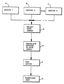
Reference is now made to the flowchart of FIG. 8. At Blocks A, B and C a
plurality
WO 95/10854 217 2 812 PCT/US94/03098
27
of circuit designs are provided. The circuit designs may be totally
independent of
one another, although two or more may receive a Gammon signal or signals, such
as clock frequency.
At Block D the plurality of designs are evaluated, using software tools
provided
by the gate array vendor, to determine (a) a total number of gates that will
be
required to implement each design, and (b) a total number of bi-directional,
input,
and output interface pins that will be required for each design. Based on
these
determinations, a gate array tyF~e is selected that has a total number of
gates that
exceeds the sum of the required gates for each design, and that also provides
a
sufficient number of interface pans to accommodate the circuit design having
the
largest required number of interface pins for a given class (bi-directional,
input,
output).
In this regard it is noted that, in the presently preferred embodiment of the
invention, the numbers of bi-di:rectional, input, and output pins are
considered
separately. However, it is also within the scope of the invention to assign
all or
most of the interface pins to be bi-directional. While this may simplify the
assignment of interface pins between the various designs that are being
accommodated, the use of a bi-directional pin will generally consume more
power
than the use of a pin defined solely as an input pin or as an output pin.
Additional
ground pins may also have to be provided as the number of bi-directional
interface
pins is increased.
At Block E each of the circuit designs is translated into a gate array
equivalent,
again using the appropriate software tools provided by the gate array vendor.
At Block F the gating block 304 is designed and translated into a gate array
equivalent. This step assumes that a sufficient number of uncommitted gates
are
available after the execution of block D.
At Block G the gate array design is fabricated and tested.
WO 95/10854 217 2 812 PCT/US94/03098
28
One suitable gate array that can be used in accordance with the teaching of
this
invention is known as an LCA10066 that is manufactured by the LSI Logic
Corporation of Milipitas, CA. This particular gate array is described in a
publication entitled "1.0 Micron Array-Based Product", (9/91 ), which is
available
from LSI Logic Corporation. Also by example, and for a cell-based array, the
various software tools that are employed to evolve initial circuit designs
into a
completed array are described in several publications that are listed on pages
iv
and v of a publication entitled "Specific Guidelines for Designs Using LSI
Logic's
Cell-Based Technology", (2/91), which is available from LSI Logic Corporation.
In the presently preferred embodiment of the invention a total of 168
interface
pins are required. The interface pins are allocated as follows.
clock input: 1 (common to all circuit blocks)
inputs: 51
outputs: 11
bi-directional: 105
The teaching of this invention takes advantage of the number of usable gates
or
cells within an array that has an adequate number of interface pins to
accommodate a given design. The combination of a multiplicity of different
circuit
blocks into a single array is achieved by partitioning a system design into
functional circuit blocks, and choosing a single package having a sufficient
number
of interface pins to accommodate a largest partition. The circuit blocks are
all
designed separately, then merged together, at the top level of the design
hierarchy,
with the decoding, multiplexing and interface pin confi~tzring circuits that
comprise the gating block 304.
There are a number of advantages that result from the use of the teaching of
this
invention. First, overall development and manufacturing costs are reduced.
Second, the use of a single array in several locations for several different
purposes
results in one higher volume part rather than several lower volume parts, thus
WO 95/10854 217 2 ~ 12 pCT~S94/03098
29
leveraging higher quantity discounts. In the presently preferred embodiment,
the
combined array design takes on one of three totally separate functions
depending
on where it is installed on the printed circuit board. The operation of the
array
is totally different for each mode, and may be represented on schematic
drawings
as several different arrays.
It should be realized that the foregoing description is not intended to limit
the
teaching of this invention. That is, a number of different types of circuit
designs
can be accommodated, other than the CDU 18, MAU 36, and MDU 38 designs that
were described in detail above. ~~urthermore, the teaching of this invention
can be
used to combine from two to some arbitrarily large number of circuit designs
within a given package, subject to constraints imposed by a total number of
available gates and a total number of interface pins that can be dedicated as
mode
select pins.
Thus, while the invention has been particularly shown and described with
respect
to a preferred embodiment thereof, it will be understood by those skilled in
the art
that changes in form and details may be made therein without departing from
the
scope and spirit of the invention.