Note: Descriptions are shown in the official language in which they were submitted.
~ wo 95/13189 ~ 2 ~ 2 ~ PCT/USg4/09652
ABRASION WEAR I~ESISTANT COATED SUBSTRATE PRODUCT
FIELD OF THE INVEN'IlON
This invention relates generally to coated substrate products.
More particularly, the invention relates to a substantially optically transparent
coated substrate product comprised of a parent substrate, one or more interlayers
and a top coating layer of substantially optically transparent, hard and low friction
m~t~ri~l, and to a method for producing same.
BACKGROUND OF THE INVENTION
The properties of glass make it an ideal substrate m~tçri~l for use in
many applications. In particular, the combination of optical transparency, with
reasonable strength at a nominal cost, allows the widespread use of glass products.
Glass, however, does suffer from several limitations. Glass is not a particularly
hard material, and consequently it abrades in many applications. Additionally,
glass is chemically reactive with many alkaline substances and with hydrofluoricacid. New applications and superior performance in existing applications could be
thus realized for glass products if glass were more abrasion resistant and less
chemically reactive. Examples of glass products which could benefit from
improved abrasion resi~t~nce include eyeglass and sl~ngl~s lenses, architecturalglass, analytical instrument windows, automotive windshields and laser bar code
scanners for use in retail stores and superm~rkets.
Diamond-like carbon films (DLC) are well known in the art and
have been recognized as potential coatings to enh~n~e the abrasion resistance ofvarious substrate materials, including glass. The DLC coatings possess excellentoptical properties and exhibit excellent resistance to abrasion and chemical attack
by various acids, including hydrofluoric acid. However, it has been found that the
DLC coahngs will impart improved abrasion resistance to a substrate only if the
adherence of the coating to the parent substrate is excellent.
WO 95/13189 ~ 1 7 2 ~ ~ 9 PCT/US94/09652
The most obvious and common approach to coating the glass
substrate is to apply the DLC coating directly onto a clean glass surface. However,
this approach often results in a DLC coating which displays poor adhesion and
therefore, poor abrasion resi~t~nce. DLC coatings are typically under significant
compressive stress. This stress greatly affects the ability of the coating to remain
adherent to the glass substrate. Additionally, glass often contains many alkali
oxides and other additives which can inhibit the bonding of the SiO2 in the glass to
the carbon atoms in the DLC coating. It is currently believed that the reaction
between the SiO~ in glass and the DLC is essential for the coating to exhibit
excellent adhesion. Therefore, less obvious methods are required to produce a
glass substrate with a highly adherent DLC~ coating which provideslexcellent
abrasion resistance.
In addition to glass substrates, many other optically transparent
substrate materials, such as sapphire, glassy-ceramics, salts (NaCl, KBr, KCl, etc.),
metal fluolides and metal oxides could benefit from a DLC coating, but contain
elements which inhibit the bonding of the DLC layer.
Many methods for depositing DLC have been demonstrated,
including radio frequency plasma deposition, ion beam sputter deposition from a
carbon target, ion beam sputtered carbon with ion beam assist, direct ion beam
deposition, dual ion beam deposition, laser ablation deposition from a carbon
target, and ion beam ~i.cte~l evaporation of carbon. Many of these prior art
techniques have been used to deposit DLC on glass substrates, however, the
emphasis of the prior art has not been on the adhesion of the DLC to the glass
substrate or on the abrasion resistance of the coated substrate product. Illustrative
are the following references: U.S. Patent Nos. 4,746,538; 4,400,410; 4,383,728;
4,504,519; 4,603,082; 4,060,660; 4,877,677; 4,569,738 and 4661409; Japanese
Patent Nos. 63/221841; 63/221840; 63/195266; 1147068; 1147067; 64--2001;
59-26906 and 51128686; European Patent Nos. DD-203903; SU1006402;
Deutchman, et al.; Proc. SPIE-Int. Soc. Opt. Eng. 1146, 124-34, 1989; Collins, et
al., Proc. SPIE-Int. Soc. Opt. Eng.. 1146, 37-47, 1989; Liou, et al., Proc. PIE-Int.
Soc. Opt. Eng. 1146, 12-20, 1989; Bubenzer, et al., Proc. DARPA Workshop
wo 95/13189 2 17 ~ 8 2 ~ PCT/USg4/09652
Diamond-Like Carbon Coat., Meeting date 1982, Issue AD-A136 766, 33-47,
edited by B. Bendow in NBS Spec. Publ. 669, 249-54, 1984; NBS Spec. Publ. 638,
482-82, 1984; Bubenzer, et al., NBS Spec. Publ. 638, 477-81, 1984; Appl. Phys.
Lett. 5~, 631-3, 1989; J. Vac. Sci. Technol A7, 2307-10, 1989; and D. Nir, Thin
Solid Films, 144, 201-9, 1986. These references do not however describe the use
of transparent interlayers to improve the adhesion of the amorphous carbon coating
to the substrate or substantially optically transparent DLC coatings with greatly
improved wear resistance for severe abrasive environmentc.
The application of low friction coatings, such as tin oxide, ~ minl~m
oxide, and boron nitride to optically transparent substrates such as glass is also
known in the prior art. However, because these materials have conventionally been
applied as thin layers, the wear resi~t~nce of the coated substrate in severe abrasive
environments has been poor. Conventional tin oxide coatings on architectural glass
or glass windows used in supermarket laser bar-code scanners constitute a prior art
example of a low friction coating on a transparent glass substrate. In this case, the
tin oxide coating (typically 2,000 Angstroms thick) provides an improvement in
wear resistance relative to the uncoated glass substrate. However, this coating is
neither hard enough, nor thick enough to provide wear resistance in severe abrasive
environments. Consequently tin oxide-coated glass windows in supelma ket laser
bar-code scanners undergo severe abrasion and must be frequently replaced.
Aluminum oxide coatings disclosed in European Patent Application #EPO 243541
(WO 87/02713) suffer from the same deficiencies.
Offenlegungsschrift DE 42 01 914 Al, having a United States
priority date of January 29, 1991, discloses and claims a scanner window
consisting of a transparent substrate, a transparent hard m~teri~l having a thiçkness
in the range of 500 Angstroms to 10 microns on the substrate, and a transparent
slippery top coat comprising DLC, diamond film, polytetrafluoroethylene (PTFE),
polyethylene (PE), tin oxide, indium oxide, silicone polymers, boron nitride,
aluminllm oxide and nlix.~ul~eS thereof deposited on the hard material. Scanner
windows that use hard materials in the disclosed lower range do not have sufficient
wear and abrasion resistance and those which use the disclosed slippery polymers
wo 95/13189 ~ 1 7 ~ 8 2 9 PCT/US94/09652 ~
such as PTFE, PE, silicone polymers and ~ ufes do not have the desired balance
of hardness and slipperiness to compete with those made in accordalce with the
present invention.
SUMMARY OF THE INVENTION
This invention provides a coated substrate product with superior
abrasion wear resistance and reduced chemical reactivity. More particularly, this
invention provides a coating of low friction diamond-like carbon, or' other optically
transparent or substantially optically transparent, hard and low friction materials to
the surface of a subst~nti~lly optically transparent substrate which is highly
adherent and exhibits greatly improved wear resistance for severe abrasive
environments. Still more particularly, this invention provides a coated substrate
with improved ease of cleaning. This invention also provides a low cost and
efficient process for producin~ a coated substrate product with superior abrasion
wear resistance. I
The disclosed abrasion wear resistant coated substrate product
subst~nti~lly reduces or elimin~tes the disadvantages and shortcomings associated
with the prior art techniques. The invention discloses a substantially opticallytransparent composite structure which comprises a parent substrate, and at least one
composite layer having a thickness of about 1 micron (,um) to about 20,um and anouter layer of diamond-like carbon or other substantially optically transparent or
optically transparent, hard and low friction material (herein referred to as a low
friction material). Examples of other low friction materials include,tin oxide,
indium oxide, boron nitride, aluminum oxide, zirconium oxide, boron carbide,
carbon nitride, molybdenum disulfide, mixtures thereof and chemically bonded
combinations thereof. The invention also discloses a method for fabricating the
coated substrate product.
According to the method, the substrate surface is iniaally chemically
de-greased. In the second step, the substrate is bombarded with energetic gas ions
to assist in the removal of residual hydrocarbons, as well as alkali metals and other
additives. After the substrate surface has been sputter-etched, one or more
interlayers are chemically vapor deposited on the substrate, followed by the
Wo 95/13189 2 ~ 7 2 8 2 9 pcTruss4lo9652
deposition of a layer of optically transparent or ,ubstantially optically transparent,
hard and low friction material. Once the requisite number of interlayers and thelow friction top layer have been deposited, the coated substrate is cooled and
removed from the reactor.
BRIEF DESCRIPTION OF THE DRAWINGS
Further features and advantages will become apparent from the
following and more particular description of the preferred embodiment of the
invention, as illustrated in the accompanying drawings, in which like reference
characters generally refer to the same parts or elements throughout the views, and
in which:
Figure 1 is a cross-sectional view of the coated substrate product in
accordance with the present invention;
Figure 2 is a cross-sectional view of the coated substrate product in
accordance with a further embodiment of the prevent invention;
Figure 3 is a cross-sectional view of the coated substrate product in
accordance with a still further embodiment of the present invention; and
Figure 4 is a graph of the ratio of scans per defect versus the
interlayer thickness of the coating of a coated bar-code scanner window product in
accordance with the present invention.
DETAILED DESCRIPTION OF THE INVENTION
In accordance with the present invention, the disclosed abrasion wear
re~i~t~nt coated substrate product subst~nti~lly reduces or elimin~tes the
disadvantages and shortcomings associated with the prior art techniques. As
illustrated in Figures 1-3, the disclosed invention is a subst~ntizllly optically
transparent composite structure which comprises a parent substrate, one or more
interme~ te layers (interlayers) and a top layer of diamond-like carbon or otherlow friction material. By the term of "substantially optically transparent", it is
intende~l to mean transparent to light in the visible region of the electromagnetic
spectrum, which is generally between 350 nanometers and approximately 750
nanometers wavelength and having an integrated tr~nsmitt~nce between 3~0
nanometers and approximately 750 nanometers of greater than approximately 10%.
WO 95/13189 PCTIUS94/09652 ~
~172~2~
-6-
General purpose sunglasses are one example of a "substantially optically
transparent" product. By the term of "optically transparent", it is intende~l to mean
having an integrated tr~n.cmitt~nce between 350 nanometers and approximately 750nanometers of greater than approximately 70%. By the term "hard", it is intendedto mean having a hardness of greater than 200kg/mm2. By the term "low friction"
is intende~l to mean having a coefficient of sliding friction of less than 0.3. A
highly important technical advantage of the invention is that the resultant
multilayer composite structure produces a highly abrasion wear resistant surface on
various substrate materials, particularly glass.
In certain optical products, such as s--ngl~ses, architectural glass,
and filters for use in analytical instrumentation, it is advantageous to reduce the
tr~n~mitt~nce of visible light over specified wavelength ranges, while still
m~int~ining some minimum amount of visible light tran~mitt~nce. For applicationssuch as these, the use of "substantially optically transparent" materi~ls is
appropliate.
For the majority of products used to transmit visible light, an
integrated optical tr~n~mitt~nce over the wavelength of 350 nm to approximately
750 nanometers greater than 50% is preferred. In this case, some materials fitting
the definition of substantially optically transparent cannot be used, and the use of
"optically transparent" materials is preferred. For applications which require an
integrated visible optical tr~n~mitt~nce over the wavelength of 350 nm to
approximately 750 nanometers of greater than 70%, the use of "optically
transparent" m~teri~l~ is most preferred. Watch crystals and eyeglass lenses areexamples of products l~uhillg the use of optically transparent m~teri~l~
The degree of optical tr~n~mitt~nce of a material is determined by
thickness, absorption coefficient, and reflectance. It is important to note that the
stoichiometry, and chemical bonding in materials can be modified by variation ofdeposition process pal~l,lelel~. In this way, a material which is "optically
transparent" in its normal stoichiometric form (e.g. aluminum oxide, Al2O3) can be
made "subst~nti~lly optically transparent" by slight alterations in stoichiometry (e.g.
AlO). While slight alterations in stoichiometry can lead to significant changes in
2~2~
WO 9S/13189 - PCT/US94/096S2
optical properties, these variations often result in a minimal or negligible effect on
the other physical or tribological properties of a material. Thus, the opticallytransparent, hard and low friction layers of the present invention can be modified,
as required by the application, to become substantially optically transparent, while
still m~int~ining their advantageous plope.lies of hardness and low friction.
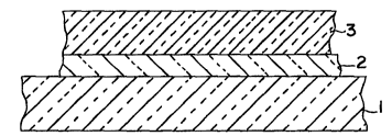
In the pl`~f~.lGd embodiment form of the invention, as illustrated in
Figure 1, a first interlayer 2 (or adhesion-m~ ting layer) is chemic~lly vapor
deposited onto a parent substrate 1 which comprises a subst~nti~lly optically
transparent amorphous material, a single crystal, polycrystalline materials, glass,
salt m~ten~l~, ceramic materials and/or mixtures thereof. By the term of
"chemically vapor deposited", it is intended to mean m~tçri~l~ deposited by
vacuum deposition processes, including thermal evaporation, electron beam
evaporation, magnetron sputtering, ion beam spulle~ g from solid precursor
materials; thermally-activated deposition from reactive gaseous precursor materials;
glow discharge, plasma, or ion beam deposition from gaseous precursor materials.Preferably, the first interlayer 2 is deposited onto the parent substrate 1 by ion
beam or magnetron sputtering.
Atmospheric pressure deposition methods including arc-spray or
plasma-spray deposition from gaseous or solid precursor materials, or
thermally-activated deposition from reactive gaseous precursor materials may
additionally be employed to deposit the first interlayer 2.
The first interlayer 2 generally comprises a subst~nti~lly optically
transparent material devoid of alkali metal atoms and fluorine, and capable of
forming a strong chemical bond to the substrate 1 and the low friction diamond-
like carbon layer 3. By the phrase of "strong chemical bond to the diamond-like
layer", it is intended to mean that the interlayer is composed of a ~i~nific~nt
amount of an element or elements which are capable of undergoing a chemical
reaction with carbon to form carbide-bonding. The absence of alkali metals and
fluorine is essential to achieve a highly adherent interface between the first
interlayer 2 and the diamond-like carbon layer 3. Thus, the first interlayer 2 must
also have the property of providing a barrier to diffusion of alkali metals and
WO 95/13189 ~ ~ 7 2 8 2 ~ PC'r/lJS94/09652
- 8 -
additives from the parent substrate 1 to the diamond-like carbon layer 3. In theplerell~,d embodiment form of the invention, the first interlayer comprises silicon
nitride, titanium nitride, tantalum nitride, hafnium nitride, zirconium nitride, boron
nitride, yttrium oxide, germanium oxide, hafnium oxide, silicon oxide, silicon
S dioxide, tantalum oxide, titanium oxide, zirconium oxide, silicon carbide,
germanium carbide, mixtures thereof and chemically bonded combinations thereof
when layer 3 is composed of diamond-like carbon. By the term "oxide", it is
intended to mean a stoichiometrically oxidized m~teri~l, or a partially oxidizedmaterial which contains excess metal atoms, or is deficient in oxygen. By the term
"nitride", it is intended to mean a material composed of a stoichiometric amount of
nitrogen or a material which either contains excess nitrogen atoms, or is deficient
in nitrogen. By the term "carbide", it is intended to mean a material composed of
a stoichiometric amount of carbon or a material which either contains excess
carbon atoms, or is deficient in carbon.
By the term "chemically bonded combinations" it is intended to
mean a combination of at least two of the foregoing materials which are joined by
chemical bonds, e.g. silicon oxide and silicon nitride to form silicon oxy-nitride.
In the case of a single interlayer, first interlayer 2 ranges from
approximately lym to 20ym in thickness. Preferably, the first interlayer 2 is from
about 5~ thick to about l}lm in those cases in which there are at least one other
interlayer.
Following deposition of the first interlayer 2 onto the parent
substrate 1, the low friction diamond-like carbon layer 3 is chemically vapor
deposited onto the coated substrate. The diamond-like carbon layer 3 can be from10 A to 20ym in thickness. Preferably, the diamond-like carbon layer 3 is at least
50 ~ thick.
To further enhance the abrasion wear resistance of the structure,
more than one interlayer or a plurality of alternating interlayers and diamond-like
carbon layers 3 may be deposited onto the parent substrate 1. It has been found
that this arrangement allows for the deposition of a greater total thickness of DLC
material, which provides a further increase in abrasion resistance. Thus, in further
Wo 95/13189 ~ J ~ 2 8 h~ ~ PCTIUS94/0~6~2
envisioned embodiments of the invention, not shown, the structure may comprise aparent substrate 1, two different and separately deposited first interlayers 2 and a
diamond-like carbon layer 3; or a parent substrate 1 and two or more pairs of first
interlayers 2 and diamond-like carbon layers 3.
5 It has unexpectedly been found that in severe wear environments, the
abrasion resict:~nce of the coated substrate product can be dr:~m:~tic~lly improved by
using a relatively thick, e. g in the range of about l~lm to about 20}1m, first
interlayer 2 between parent substrate 1 and low friction DLC layer 3. Such a
highly abrasion wear resistant and corrosion resistant coated substrate product is
obtained by depositing such a relatively thick film of at least one interlayer 2having a hardness greater than that of substrate 1 and then depositing a
comparatively thin, e.g. at least 50 ~, layer of DLC as the top coat. In addition to
serving as the bonding layers between substrate 1 and DLC top layer 3,
interlayer(s) 2 provide a hard "structural support layer" for DLC layer 3. The
thinner DLC top most layer provides a low friction, corrosion-resi~t~nt, protective
surface for the substrate. The resulting coated substrate product has greater
commercial utility than similar products in which the substrate is deposited with
thin interlayer(s) 2 followed by a relatively thick DLC layer 3 in the following two
cases. The first case is if the optical absorption coefficient of DLC layer 3 is too
high to allow a thick DLC layer to be deposited while simult~neously meeting
stringent optical transparency requir~ ellts for the coated product. The second
case is if the deposition rate of DLC layer 3 is much lower than that of
interlayer(s) 2, using a thick interlayer 2 to achieve the required degree of abrasion
resi~t~nce is more economical than using a thick DLC layer 3.
It has also been unexpectedly found that low friction materials other
than diamond-like carbon can be applied as top layers over the relatively thick
interlayers to produce a product with dramatically improved wear resistance in
severe abrasive environments. In this case, a low friction m~t~ri~l chosen from tin
oxide, indium oxide, aluminum oxide, zirconium oxide, boron nitride, boron
carbide, molybdenum disulfide, carbon nitride, mixtures thereof and chemically
bonded combinations thereof, or other optically transparent or subst~nti~lly
Wo 95/13189 PCT/US~4/0~652 ~
2 9
-10-
optically transparent, hard and low friction materials is deposited a$ the top layer 3
over interlayers in the thickness range of lym to approximately 20ym, which havebeen deposited onto the parent substrate. A highly abrasion wear resistant coated
substrate product is obtained by depositing such a relatively thick film of at least
one interlayer 2 having a hardness greater than that of substrate 1 and then
depositing a comparatively thin, e.g. at least soA, layer of low friction material as
the top coat. In addition to serving as the bonding layers between substrate 1 and
the low friction top layer 3, interlayer(s) 2 provide a hard "structural support layer"
for low friction layer 3. The thinner top layer 3 provides a low friction, protective
surface for the substrate. The use of low friction layers of tin oxide, indium oxide,
aluminum oxide, zirconium oxide, boron nitride, boron carbide, molybdenum
disulfide, carbon nitride, n~ ulcs thereof and chemically bonded combinations
thereof, or other optically transparent or substantially optically transparent, hard
and low friction materials is advantageous compared to the use of diamond-like
carbon in the following two situations. The first situation is one in which the
special deposition equipment (ion beam source, plasma source, laser deposition
source, and the like) required for the production of diamond-like carbon is not
available. The second situation is if the optical absorption coefficient of a DLC
layer is too high to allow the required thickness of DLC to be used while meeting
stringent optical transparency requirements for the coated product., For example,
this situation can be encountered even for very thin (i.e. 100 A thick) DLC layers
when an optically "water clear" coating is required. Normally, apFlication of DLC
layers even as thin as 100 A will cause a yellow, orange, or light brown coloration
of the coated substrate when viewed in tr~n~mi~sion. I
A key feature of the present invention is that the low friction
materials are specified not be from the class of materials generally known in the
prior art as "polymers." Examples of low friction polymer materials include
polyethylene, polytetrafluoroethylene (PTFE) ("Teflon(g)") and conventional silicone
polymers. All of the conventional low friction polymer materials are soft by
comp~ on to the low friction layers of the present invention. Because of their
low hardness, these polymer materials are susceptible to d~m~ge by scratching or
~ wo 9~/13189 2 ~ 7 2 ~ 2 9 PCTIUS94/09652
scraping off of the interlayer, hence a coated product with improved abrasion
resistance in severe abrasive environmentc is not achieved.
In the case in which low friction layer 3 is composed of tin oxide,
indium oxide, aluminum oxide, zirconium oxide, boron nitride, boron carbide,
S molybdenum disulfide, carbon nitride, ~ ules thereof and chemically bondedcombinations thereof, or other optically transparent or substantially optically
transparent, hard and low friction materials, then interlayer 2 may comprise a
subst~nti~lly optically transparent material of silicon nitride, titanium nitride,
tantalum nitride, hafnium nitride, zirconium nitride, boron nitride, yttrium oxide,
germanium oxide, silicon dioxide, tantalum oxide, titanium oxide, zirconium oxide,
hafnium oxide, silicon oxide, silicon carbide, germanium carbide, alllminllm oxide,
aluminum nitride, cerium oxide, tin oxide, indium oxide, thorium oxide, lithium
oxide, sodium oxide, potassium oxide, rubidium oxide, cesium oxide, francium
oxide, beryllium oxide, magnesium oxide, calcium oxide, strontium oxide, cerium
oxide, radium oxide, barium fluoride, cerium fluoride, magnesium fluoride, thorium
fluoride, calcium fluoride, neodymium fluoride, lead fluoride, sodium fluoride,
lithium fluoride, zinc selenide, zinc sulfide, mixtures thereof and chemically
bonded combinations thereof. Because of their high hardness, materials for
interlayer 2 are preferably silicon nitride, zirconium nitride, boron nitride, yttrium
oxide, silicon oxide, silicon dioxide, zirconium oxide, silicon carbide, aluminum
oxide, aluminum nitride, mixtures thereof and chemically bonded combinations
thereof. Most preferably, interlayer 2 is composed of silicon oxy-nitride. In nocase would the low friction layer 3 and the interlayer 2 which is bonded directly to
low friction layer 3 be chosen from the same material.
In another embodiment of the invention, as illustrated in Figure 2, a
second interlayer 4 is chemically vapor deposited onto the coated substrate and
positioned such that the second interlayer 4 is disposed between the first interlayer
2 and the low friction diamond-like carbon layer 3. The second interlayer 4 would
similarly comprise a substantially optically transparent material devoid of alkali
metal atoms and fluorine, and capable of forming a strong chemical bond to the
first interlayer 2 and the low friction diamond-like carbon layer 3. The second
WO 95/13189 2 :L 7 ~ ~ ~ 9 PCT/US9~/09652
-12-
interlayer may comprise a subst~nti~lly optically transparent silicon nitride,
titanium nitride, tantalum nitride, hafnium nitride, zirconium nitride, boron nitride,
yttrium oxide, germ~ni--m oxide, hafnium oxide, silicon oxide, silicon dioxide,
tantalum oxide, titanium oxide, zirconium oxide, silicon carbide, germanium
S carbide, ~ ules thereof and ch~mi~lly bonded combinations thereof when the
low-friction layer 3 is diamond-like carbon.
Since the second interlayer 4 provides a diffusion barrier for alkali
metal atoms, fluorine and/or any additional additives which would adversely effect
the adherence of the low friction diamond-like carbon layer 3, the first interlayer
could further comprise a substantially optically transparent aluminum oxide, cerium
oxide, tin oxide, indium oxide, thorium oxide, lithium oxide, sodium oxide,
potassium oxide, rubidium oxide, cesium oxide, francium oxide, beryllium oxide,
m~nesium oxide, calcium oxide, strontium oxide, cerium oxide, radium oxide,
barium fluoride, cerium fluoride, ma~nesium fluoride, thorium fluoride, calcium
lS fluoride, neodymium fluoride, lead fluoride, sodium fluoride, lithium fluoride, zinc
selenide, zinc sulfide, mixtures thereof and chemically bonded combinations
thereof.
In yet another embodiment of the invention, if low friction layer 3 is
composed of tin oxide, indium oxide, aluminum oxide, zirconium oxlde, boron
nitride, boron carbide, molybdenum disulfide, carbon nitride, Illi~LulcS thereof and
chemically bonded combinations thereof, or other subst~nti~lly optically
transparent, hard and low friction materials, then interlayers 2 and 4 may comprise
a subst~nti:~lly optically transparent material of silicon nitride, tit~nillm nitride,
t~nt~hlm nitride, hafnium nitride, zirconium nitride, boron nitride, yttrium oxide,
germanium oxide, hafnium oxide, silicon oxide, silicon dioxide, tantalum oxide,
LiLaniulll oxide, zirconium oxide, silicon carbide, ~errn~nium carbide, al-lminllm
oxide, aluminum nitride, cerium oxide, tin oxide, indium oxide, thorium oxide,
lithium oxide, sodium oxide, potassium oxide, rubidium oxide, cesium oxide,
francium oxide, beryllium oxide, ma~nesium oxide, calcium oxide, sLIollLiulll oxide,
cerium oxide, radium oxide, barium fluoride, cerium fluoride, magnesium fluoride,
thorium fluoride, calcium fluoride, neodymium fluoride, lead fluoride, sodium
wo 95/13189 ~ 3 7 2 8 2 ~ PCT/US94/09652
fluoride, lithium fluoride, zinc selenide, zinc sulfid~, mixtures thereof and
chemically bonded combinations thereof. Because of their high hardness, materials
for interlayers 2 and 4 are preferably silicon nitride, zirconium nitride, boronnitride, yttrium oxide, silicon oxide, silicon dioxide, zirconium oxide, siliconcarbide, aluminum oxide, aluminum nitride, mixtures thereof and chemically
bonded combinations thereof. Most preferably, interlayer 2 and/or interlayer 4 is
composed of silicon oxy-nitride. In no case would the low friction layer 3 and the
interlayer which is bonded directly to low friction layer 3 be chosen from the same
material.
The second interlayer 4 can be from 5 ~ to 20,um in thickness.
Preferably, second interlayer 4 is at least 10 ~ thick. Still more preferably, second
interlayer 4 has a thickness in the range of 1,um to 20,um in the case in which the
thickness of first interlayer(s) 2 is in the sA to lpm range, or second interlayer 4
has a thickness in the ran~e of 5 ~ to 1 ym in the case in which the thickness of
first interlayer(s) 2 is in the 1 pm to 20 pm range to achieve the unexpected results
of greatly improved abrasion resistance in severe wear environments for the coated
substrate product.
To further enhance the abrasion wear resistance of the coating
structure, more than one interlayer, or a plurality of interlayers, with an optically
transparent or subst~nti~lly optically transparent, hard, and low friction outer layer
3 may be deposited onto the parent substrate 1. In this way, it is often possible to
deposit a greater total thickness of hard interlayer material, while m~int~ining good
adhesion of the coating, providing a further increase in abrasion resistance. One
example of this would be a glass substrate coated with a 1,000 ~ thick first
interlayer of silicon dioxide, then three pairs of alternating layers of 0.5 pm thick
silicon oxy-nitride and 0.5 ,um thick aluminum oxide (silicon oxy-nitride/~lnminllm
oxide/ silicon oxy-nitride/aluminum oxide/ silicon oxy-nitride/~ minl-m oxide),
followed by a 500 ~ thick top layer of optically transparent tin oxide. In this case,
although each individual interlayer is less than l~m thick, the sum total thickness
of all the interlayers is 3.1 ym, and the composite coating layer thickness is 3.15
,um, resulting in a product with improved wear resistance in severe abrasive
WO 95/13189 PCT/US94/09652
2 ~ 2 ~
-14- 1
environments according to the present invention. Similarly, each of the silicon
oxy-nitride and aluminum oxide layers above could be greater than 1 ,um thick, so
that the sum total thickness of all the interlayers is 6.1 ym, and the compositecoating layer thickness is 6.15 ,um, resulting in a product with even further
S improved wear resi~t~nce in severe abrasive en~ironn,ellts. Thus, in further
envisioned embodiments of the invention, not shown, the coating layer structure
may comprise a parent substrate 1, two or more dir~ t and separately deposited
interlayers (2,4) and a low friction outer layer 3; or a parent substrate 1 a first
interlayer 2, two or more pairs of interlayers (4) and a low friction outer layer 3.
In the case where the low friction layer 3 is diamond-like carbon,
the second interlayer 4 may alternatively comprise a substantially optically
transparent metallic material capable of reflecting visible light and capable offorming a strong chemical bond with the first interlayer 2 and the low friction
diamond-lil~e carbon layer 3, selected from the following two groups. In the first
group, the metallic material may consist of silicon, germanium, hafnium,
molybdenum, tungsten, yttrium, tantalum, titanium and zirconium. These metallic
materials all form a strong chemical bond to the low friction diamond-like carbon
layer 3.
The second group of metallic materials comprises vanadium,
niobium, chromium, manganese, rhenium, technetium, iron, cobalt, iridium,
rhodium, nickel, palladium, platinum, copper, silver, gold, zinc, ruthenium, indium,
aluminum, tin, osmium, thallium, lead, antimony, bismuth and polonium. Among
the second group of metallic materials, rhenium, iridium, tin, indium, aluminllm,
nickel, iron, chromium, copper, ~old, silver and platinum are preferable as second
interlayer 4. Although these materials will provide a diffusion barrier to aLkali
metal atoms and fluorine, they will not form a strong carbide bond with the low
friction diamond-like carbon layer 3. Therefore, if any of these second group
metallic materials are selected for the second interlayer 4, a third interlayer (not
shown) must be disposed between the second interlayer 4 and the low friction
diamond-like carbon layer 3. The third interlayer would similarly comprise a
subst~nti~lly optically transparent material devoid of alkali metal atoms and
WO 95/13189 ~ 17 2 ~ ~ !3 PCT/US9-1/09652
-15-
fluorine and selected from the group consisting of silicon nitride, titanium nitride7
tantalum nitride, hafnium nitride, zirconium nitride, boron nitride, yttrium oxide,
geranium oxide, hafnium oxide, silicon oxide, silicon dioxide, tantalum oxide,
titanium oxide, zirconium oxide, silicon carbide, germanium carbide, mixtures
thereof, and chemically bonded combinations thereof. Although it is not necessary,
this third interlayer may be employed with the aforementioned first group of
metallic materials.
In the case where the low friction top layer 3 is composed of tin
oxide, indium oxide, aluminum oxide, zirconium oxide, boron nitride, boron
carbide, molybdenum disulfide, carbon nitride, mixtures thereof and chemically
bonded combinations thereof or other optically transparent or substantially optically
transparent, hard, and low friction materials, substantially optically transparent
metallic materials selected for interlayer 4 may comprise silicon, gelm~nium,
hafnium, molybdenum, tungsten, yttrium, tantalum, titanium, zirconium, v~n:l-linm,
lS niobium, chlu,l-iulll, manganese, rhenium, technetium, iron, cobalt, iridium,
rhodium, nickel, p~ rlillm, platinum, copper, silver, gold, zinc, ruthenil-m, inr1inm,
aluminum, tin, osmium, thallium, lead, antimony, bismuth and polonium. Among
these metallic materials, rhenium, iridium, tin, indium, alllminllm, nickel, iron,
chromium, copper, gold, silver, platinum, silicon, germanium, molyWenum,
tungsten, titanium, tantalum, and zirconium are ~lert;ll-,d.
The metallic second interlayer 4 can be from 5 A to lOOOA in
thickness Preferably, the met~llic second interlayer 4 is at least 10 A thick.
In yet another embodiment of the invention, as illust~te(l in Figure
3, the embodiment illustrated in Figure 2 and discussed above is provided with asecond composite layer comprising a first interlayer 2 and a low friction
diamond-like carbon layer 3. The resultant multilayer structure would thus be a
parent substrate 1, a first interlayer 2, a second interlayer 4, a diamond-like carbon
layer 3, a first interlayer 2 and a diamond-like carbon layer 3. The structure may
alternatively comprise a parent substrate 1, two first interlayers 2, a diamond-like
carbon layer 3, a first interlayer 2 and a diamond-like carbon layer.
-
WO 95/13189 PCT/US94/09652 ~
2 ~
-16-
By choosing the appropriate interlayer 2, 4 and low friction
diamond-like carbon layer 3 thicl~nesses, criteria which are known in the art ofoptical coating design could be employed in each of the aforementioned
embodiments of the present invention to produce quarter wavelength stacks and
other "dielectric stack" coating configurations. In these dielectric stack
configurations, optical intGl~r~ilce effects could be used to produce
wavelength-selective mirrors or anti-reflection films. By choosing the appropriate
thickness of at least one of the interlayers 2, 4 and diamond-like carbon layer 3,
the reflection of light at predetermined wavelength ranges may be either minimi~or maximized. Superior abrasion wear re~ t~nce and environmental durability
currently unavailable with conventional optical coatings could thus be realized by
the incorporation of the dielectric stack configurations into the present invention.
The method of the present invention teaches those skilled in the art
how to fabricate the transparent abrasion wear resistant coated substrate product.
According to the method, the first step involves chemically de-greasing the surface
of the parent substrate 1. The substrate 1 is then placed into a chemical vapor
deposition reactor vacuum chamber and the air evacuated from the chamber to lessthan approximately 5 x 10⁻⁶ Torr.
In the next step the surface of the substrate 1 is sputter etched with
energetic ions or atoms to assist in the removal of residual hydrocarbons, as well
as alkali metals and other additives which are commonly present on the surface of
the substrate materials, particularly glass. It has been found that the concentration
of alkali metals (Na, Ca) at the surface of glass substrates was signific~ntly
reduced as a function of ion sputter-etching time and that increased sputter-etching
2~ time substantially improved the adhesion of the low friction diamond-like carbon
layer 3. [See Examples A-Z]. Therefore, it is concluded that the removal of alkali
metals and other additives is essential to a achieve a highly adherent interfacebetween parent substrate 1 and the low friction diarnond like carbon layer 3.
The sputter-etching may be performed with a beam of inert gas ions,
hydrogen ions or oxygen ions, a glow discharge or a plasma of inert gas, hydrogen
WO 95/13189 ~ PCT/USg4109652
or oxygen. In the preferred embodiment form of the invention, sputter-etching isperformed with a beam of energetic gas ions at an energy of at least 200 e~.
Following the sputter-etching step one or more interlayers are
chemically vapor deposited onto the parent substrate 1. During a first cycle any of
the aforementioned conventional chemical vapor deposition methods may be
employed to deposit the interlayers 2, 4 (Fig. 2 & 3). The deposition rate of each
interlayer 2,4 is generally in the range of about 0.1-10 microns/hour. The totalthickness of each interlayer can be in the range of about 5 ~ to 20,um. In the
preferred embodiment of the invention, the thickness of at least one interlayer is in
the range of about 1,um to 20~m and the total thickness for each of the other
interlayers is at least 10 A.
After the chemical vapor deposition of one or more interlayers onto
the parent substrate 1, a low friction layer 3 is deposited onto the coated substrate.
Diamond-like carbon layer 3 can be deposited by the following conventional
methods: (i) direct ion beam deposition, dual ion beam deposition, glow discharge,
RF-plasma, DC-plasma, or microwave plasma deposition from a carbon-cont~.ining
gas or a carbon- containing vapor which can also be mixed with hydrogen,
nitrogen-co~t:~ining gases, oxygen containing gases and/or inert gas, (ii) electron
beam evaporation, ion-,.csicted evaporation, magnetron sputtering, ion beam
sputterin~, or ion-assisted sputter deposition from a solid carbon target material, or
(iii) combinations of (i) and (ii).
In the preferred embodiment form of the invention, the low friction
diamond-like carbon layer(s) is deposited by ion beam deposition from a
hydrocarbon gas or carbon vapor. The ion beam deposition may also be performed
in combination with an inert gas or hydrogen.
Low friction layers of tin oxide, indium oxide, al-lminllm oxide,
zirconium oxide, boron nitride, boron carbide, molybdenum dis~llfide, carbon
nitride, mixtures thereof and chemically bonded combinations thereof, or other
optically transparent or subst~ntially optically transparent, hard and low friction
materials can be deposited by the following methods: (i) direct ion beam
deposition, glow discharge, RF-plasma, D(:~-plasma, or microwave plasma
WO 95/13189 PCT/US94/09652 ~
2 ~
-18-
deposition from vapors composed at least partially of the elements contained in the
low friction layers, (ii) electron beam evaporation, ion-assisted evaporation,
magnetron sputtering, ion beam sputtering, or ion-~c~i~te-l sputter deposition from a
solid target material, or (iii) combinations of (i) and (ii). In the prert;ll~d
embodiment form of the invention, the low friction layers are deposited by ion-
assisted evaporation, magnetron sputtering, or ion beam sputtering.
The deposition rate of the low friction layer 3 is generally in the
range of about 0.1-10 microns/hour. The total thickness of the low friction layer is
generally in the range of about 10 A to 20ym. If the thickness of low friction
layer 3 is greater than approximately 1 micron, then the hardness of layer 3 should
be greater than the hardness of the substrate material. Preferably, the thickness of
the low friction layer 3 is at least 50 ~ thick.
After the deposition of the applopliate interlayers and low friction
layer(s) 3, as detailed in the aforementioned embodiments, the coated substrate
product is cooled by extinguishing the deposition process and passi4g an inert gas
over the substrate until it has reached subst~nti~lly room temperature. The coated
substrate product, exhibiting superior abrasion wear resistance, is then removedfrom the reactor.
The examples which follow illustrate the superior performance of the
invention. The examples are for illustrative purposes only and are not meant to
limit the scope of the claims in any way.
Example A
A 2" x 2" x 0.375" thick float glass plate was cut from a glass bar
code scanner window and coated by the following procedure. The glass plate was
chemically cleaned by trichloromethane followed by methanol solvents in an
ultrasonic bath. The sample was removed and blown dry with nitrogen gas. The
glass plate was then mounted onto a substrate holder and part of the substrate
surface was m~kecl The sample was then inserted into a vacuum chamber which
was then evacuated to 8 x 10⁻⁷ Torr. The sample was sputter-etched for 1 minute
by a beam of Ar+ ions at an energy of 500 ev and a current density of 0.5 mA/cm2.
The sample was then coated by direct ion beam deposition using an 11 cm ion
WO 9S/13189 PCT/US94/09652
2172~
-19-
beam source operated on CH4 gas at a p,es~ule of 7.2 x 10 5 Torr. The ion energywas 75 eV and the ion beam current density was 0.30 mA/cm2. A transparent
coating of 3000 ~ thickness was deposited. The sample was removed and
scratch-tested by rubbing a sharp piece of glass or a glass jar across the interface
S between the coated and uncoated (m~c~) areas. While the uncoated area showed
deep and wide scratches, no sc;,~lches were observed on the DLC-coated area. Thecoating was tested for adhesion by alternately illllll.~.sirlg the sample in baths of
boiling water (for 2 minutes) and ice water (for 2 minutes). After one thermal
cycle, the coating peeled off of the glass substrate.
Example B
A 2" x 2" x 0.375" thick float glass plate was chemically cleaned,
mounted, m~ke~l, and ion sputter-etched in vacuum for 10 minutes by the
procedure described in Example A. Next, a 100-A thick layer of SiO2 was
deposited onto the glass plate b~ Ar+ ion beam sputter deposition from a quartz
lS target. Then, a diamond-like carbon layer of 3,000 ~ thickness was deposited by
the method described in Example A. The coating could not be scratched when
rubbed by a sharp piece of glass or a glass jar. The coating rçln~ine 1 adherentafter S thermal cycles b~Lween boiling water and ice water.
Example C
A 2" x 2" x 0.375" thick float glass plate was chemically cleaned,
mounted, m~c~l, and ion sputter- etched in vacuum by the procedure described in
Example B. Next, a 1,000-A thick layer of SiO2 was deposited onto the glass plate
by Ar+ ion beam sputter deposition from a quartz target. Then, a diamond-like
carbon layer of 3,000 A thickness was deposited by the method descAbed in
Example A. The coating could not be scratched when rubbed by a sharp piece of
glass or a glass jar. The coating remained adherent after 5 thermal cycles between
boiling water and ice water.
Example D
A 2" x 2" x 0.375" thick float glass plate was chemic~lly cleaned,
mounted, m~c~ecl, and ion sputter-etched in vacuum by the procedure descAbed in
Example B. Next, a the coating described in Example B was repeated three times
WO 95/13189 PCT/US94/09652
~7~8~9
-20-
in sequence, so the total coatin~ thickness deposited onto the glass plate was 9,300
A. The coating could not be scratched when rubbed by a sharp piece of glass or aglass jar. The coating r~m~ined adherent after S therrnal cycles between boilingwater and ice water.
S Example E
A 2" x 2" x 0.375" thick float glass plate was chemically cleaned,
mounted, m~.cked, and ion sputter-etched in vacuum by the procedure described inExample A, except the sputter-etching time was 5 minut~s Next, a 800 A thick
layer of Al2O3 was deposited onto the glass plate by Ar+ ion beam sputter
deposition from an aluminum oxide target. Then, a diamond-like carbon layer of
200 A thickness was deposited by the method described in Examplel A. The
coating could not be scratched when rubbed by a sharp piece of glass. After 24
hours, the coating peeled off the substrate.
Example F
A 1" cli~meter x .06" thick soda lime glass disk was c,hemically
cleaned, mounted, m~skecl, and ion sputter-etched in vacuum by the procedure
described in Example A. Next, a 10,000 A thick layer of Al2O3 was deposited
onto the glass plate by Ar+ ion beam sputter deposition from an aluminum oxide
target. Then, a 300-A thick layer of SiO2 was deposited over the Al2O3 layer by
Ar+ ion beam sputter deposition from a quartz target. Next, a diamond-like carbon
layer of 200 A thickness was deposited by the method described in Example A.
The coating could not be scratched when rubbed by a sharp piece of glass. After S
thermal cycles between boiling water and ice water, the coating rem~in~A adherent.
Example G
A 6" x 6" x 0.375" thick float glass plate was initially coated wi~
about 2,000 A of SnO2 by thermally activated deposition from an organo-tin
compound. The plate was then chemically cleaned by the procedure described in
Example A, mounted, masked, and in~t~llçd into a vacuum chamberlwhich was
then evacuated to 3.5 x 10⁻⁶ Torr. The sample was sputter-etched for 2 minutes by
a beam of Ar+ ions at an energy of S00 eV and a current density of 0.5 mA/cm2.
Next, a 1,000-A thick layer of SiO2 was deposited over the SnO2 layer by Ar+ ion
~.~728~9
WO 95/13189 PCT/US94/09652
-21 -
beam sputter deposition from a quartz target. Then, a diamond-like carbon layer of
2,000 ~ thickness is deposited by the method described in Example A. After 5
thermal cycles between boiling water and ice water, the coating remained adherent.
Example H
A 6" x 6" x 0.375" thick float glass plate coated with about 2,000 A
of SnO2 was chemically cleaned by the procedure described in Example A,
mounted, masked, and installed into a vacuum chamber which was then evacuated
to 6 x 10⁻⁷ Torr. The sample was sputter-etched for 2 minutes by a beam of Ar+
ions at an energy of 500 eV and a current density of 0.5 mA/cm2. Then, a
diamond-like carbon layer of 2,000 A thickness was deposited by the method
described in Exarnple A. During deposition, the DLC coating began to peel off of the substrate, inAic~ting poor adhesion.
Example I
A 27 mm diameter x 2 mm thick sapphire window was
ultrasonically cleaned in trichloromethane, followed by acetone, and then methanol,
and blown dry with nitrogen gas. The sapphire sample was mounted into the
vacuum coating system and, after evacuation, sputter-etched for 3 minutes as
described in Example A. Then, a 1000-A thick layer of diamond-like carbon was
deposited onto the sapphire substrate using the conditions described in Example A.
A powdery carbon material was observed on the surface of the substrate upon
removal from the coating chamber indicating that the coating was not adherent.
Example J
A 27 mm di~me~er x 2 mm thick sapphire window was cleaned,
mounted into a vacuum coating system, evacuated, and sputter-etched for 1 minuteusing the conditions described in Example A. Then, a 100-A thick layer of SiO2
was deposited onto the sapphire substrate using the conditions described in
Example B. Next, a transparent, 1000-~ thick layer of diamond-like carbon was
deposited onto the sapphire substrate using the conditions described in Example A.
The diamond-like carbon coating was very adherent, and could not be scratched
with 50-micron quartz powder.
Example K
W O 95/13189 PCT~US94/09652
~72~29
-22-
A 27 mm diameter x 2 mm thick sapphire window w s cleaned,
mounted into a vacuum coating system, evacuated, and sputter-etched for 1 minuteusing the conditions described in Example A. Then, a 50-A thick layer of Si was
deposited onto the sapphire substrate by Ar+ ion beam sputter deposition from a Si
target. Next, a transparent, 1000-A thick layer of diamond-like carbon was
deposited onto the sapphire substrate using the conditions described lin Example A.
Subsequent optical spectroscopy analysis of the coating revealed that the Si layer
had been converted into a transparent layer of SiC by this process. The
diamond-like carbon coating was very adherent, and could not be scratched with
50-micron quartz powder.
Example L
A 130 mm diameter x 1 mm thick aluminosilicate disk was mounted
into a vacuum coating system, evacuated, and sputter-etched for 5 minutes, usingthe conditions described in Example A. Then, a 100-~ thick layer of SiO2 was
deposited onto the aluminosilicate substrate using the conditions described in
Example B. Next, a 150-~ thick layer of diamond-like carbon was deposited onto
the aluminosilicate substrate using the conditions described in Example A. The
coating was very adherent, and could not be scratched with a sharp piece of glass.
Example M
A 5.5" x 5.5" x 0.18" thick plate of Corning Code
#9984-Pyroceram(~) (Note: Pyroceram(~ is a glass/ceramic material composed at
least of rutile, aluminum oxide, and m~gnç~ium silicate.) was cleaned in isopropyl
alcohol, blown dry with nitrogen gas, mounted into a vacuum coating system,
evacuated, and sputter-etched for 15 minlltes using the conditions dèscribed in
Example A. Then, a 200-~ thick layer of SiO2 was deposited onto the substrate asdescribed in Example B. Next, a transparent, 2000-A thick layer of diamond-like
carbon was deposited onto the substrate using the conditions described in Example
A. The coating was very adherent, and could not be scratched by a sharp piece ofglass.
Example N
-
~7~29
WO 95/13189 PCTIUS94/09652
A 5.5" x 5.5" x 0.18" thick plate of borosilicate glass was cleaned in
isopropyl alcohol, blown dry with nitrogen gas, mounted into a vacuum coating
system, evacuated, and sputter-etched for 15 minutes using the conditions described
in Example A. Then, a 200-A thick layer of SiO2 was deposited onto the substrateas described in Example B. Next, a transparent, 2000-A thick layer of
diamond-like carbon was deposited onto the substrate using the conditions
described in Example A. The coating was very adherent, and could not be
scratched by a sharp piece of glass.
Example O
A 2" x 2" x 1/4" thick piece float glass and a 70 mm ~ meter x 3
mm thick neutral gray glass sunglass lens were ultrasonically cleaned in
isopropanol, and blown dry with nitrogen gas. The substrates were mounted into
the vacuum coating system and, after evacuation, sputter-etched for 5 rninutes as
described in Example A. Then, a 100-~ thick layer of SiO2 was deposited onto thesubstrates using the conditions described in Example B. Next, a 100-A thick layer
of Si was deposited on top of the SiO2 layer by Ar+ ion beam sputter deposition
from a Si target. Finally, a l,000-A thick layer of transparent ~ mon~l-like carbon
was deposited on top of the Si layer using the conditions described in Example A.
The coating was very adherent, and could not be scratched with a sharp piece of
glass which could easily scratch the un-coated glass substrates. The coating on the
s-ln~ lens exhibited an intense blue-purple reflected color.
ExamPle P
A 2" x 2" x 1/4" thick piece of float glass and a 70 mm diameter x
3 mm thick neutral gray glass sllngl~s lens were ultrasonically cleaned in
isopropanol, and blown dry with nitrogen gas. The substrates were mounted into
the vacuum coating system and, after evacuation, sputter-etched for 5 min~tes asdescribed in Example A. Then, a 100-A thick layer of SiO2 was deposited onto thesubstrates using the conditions described in Example B. Next, a 100-A thick layer
of Cr metal was deposited by Ar~ ion beam sputter deposition from a Cr target.
Next, a second 100-~ thick layer of SiO2 was deposited on top of the Cr layer.
Finally, a 1,000-A thick layer of transparent diamond-like carbon was deposited on
Wo 95/13189 PC!TIUS94/09652 ~
2172~29
-24-
top of the SiO~ layer usin the conditions described in Example A. The coating
was very adherent, and could not be scratched with a sharp piece of glass which
could easily scratch the un-coated glass substrates. The coating on the sunglasslens exhibited a bright blue reflected color.
ExamPle Q
An adherent, abrasion-resistant quarter-wavelength st-.ck reflecting
coating was formed on glass substrates. The layer thicknesses were, chosen to
maximize reflectance at a wavelength of 450 nanometers. The refractive index of
the deposited SiO2 layers was about 1.5, and the refractive index of the deposited
DLC layers was about 2.05. The coating was formed as follows:
A 2" x 2" x 1/4" thick piece of float glass and a 70 mm ~ eter x
3 mm thick neutral gray glass sunglass lens were ultrasonically cleaned in
isopropanol, and blown dry with nitrogen gas. The substrates were mounted into
the vacuum coating system and, after evacuation, sputter-etched for l5 minutes as
described in Example A. Then, a 7sO-A thick layer of SiO2 was deposited onto thesubstrates using the conditions described in Example B. Next, a 550-A thick layer
of transparent diamond-like carbon was deposited on top of the first SiO2 layer
using the conditions described in Example A. Next, a 750-A thick layer of SiO2
was deposited on top of the first DLC layer using the conditions de$cribed in
Example B. Finally, a 550-A thick layer of transparent diamond-like carbon was
deposited on top of the second SiO2 layer using the conditions described in
Example A. The coating was very adherent, and could not be scratched with a
sharp piece of glass which could easily scratch the un-coated glass substrates. The
coating exhibited a light yellow-blue reflected color on the sunglass lens, and a
light blue reflected color on the glass plate.
Example R
A 5.7" x 5.7" x 0.375" soda-lime, float glass plate was cleaned with
soap and water followed by rinsing with isopropanol and drying with nitrogen gas.
The glass plate was mounted onto a substrate holder which was in a vacuum
chamber. The vacuum chamber was then evacuated to a pressure of 5 x 10⁻⁶ Torr.
Next, the sample was sputter-etched for 10 minutes with a beam of Ar+ ions at an
WO 95/13189 ?~ 17 2 8 2 9 PCT/US94/09652
-25 -
energy of 500 eV and a current density of 0.5 mA/cm~. A 3000-~ layer of SiO2
was then deposited by ion beam sputter deposition by bombarding a silica target
with a beam of N2+ ions. Next a l-micron layer of "silicon oxy-nitride" was
deposited onto the glass plate by bombarding a Si target with a beam of N2+ ions in
the presence of air. After deposition of the silicon oxy-nitride, a loOA thick layer
of diamond-like carbon was deposited using a 11 cm ion beam source operated on
methane gas at a pressure of 1.4 x 10⁴ Torr. The beam energy was 75 eV and the
beam current density was 0.3 mA/cm2. The coating was very adherent to the glass
substrate.
Example S
A 5.7" x 5.7" x 0.375" float glass substrate was cleaned and
mounted in a vacuum chamber as in Example R. The chamber was evacuated to a
pressure of 5 x 10⁻⁶ To;r. The sample was ion beam sputter-etched as in Example
R. Next, a 3000-~ SiO2 layer was deposited as in Example R. Then, a 2-micron
silicon oxy-nitride layer was deposited as described in Example R. Finally, a 100-
DLC layer was deposited as in Example R. The coating was very adherent to
tne glass substrate.
Example T
A 5.7" x 5.7" x 0.375" float glass substrate was cleaned and
mounted in a vacuum chamber as in Example R. The chamber was evacuated to 4
x 10 6 Torr. The sample was ion beam sputter-etched as in Example R. Next, a
3000-~ SiO2 layer was deposited as in Example R. Then, a 3-micron silicon oxy-
nitride layer was deposited as descri'oed in Example R. Finally, a 100-~ DL~
layer was deposited as in Example R. The coating was very adherent to the glass
substrate.
Example U
5.7" x 5.7" x 0.375" float glass substrate was cleaned and mounted
in a vacuum chamber as in Example R. 'rhe chamber was evacuated to 4 x 10 6
- Torr. The sample was ion beam sputter-etched as in Example R. Next, a 3000-~
SiO2 layer was deposited as in Example R. Then, a 4-micron silicon oxy-nitride
wo 95/13189 PCT/US~4~ G52 ~
8 ~ ~
-26-
layer was deposited as described in Example R. A 100-A DLC layer was
deposited as in Example R. The coating was very adherent to the glass substrate. Example V
Four neutral gray ~,llpc,ed sungl~c~ lenses were cleaned by the
chemical cleaning procedure used in Example R. The lenses were subsequently
mounted onto a ~raphite plate. One-half of the surface was m~3~kecl, The graphite
plate was then mounted in a vacuum chamber and the chamber was evacuated to 5
x 10-6 Torr. The lenses were Ar+ ion beam sputter-etched as in Example R. Then,
a 3000-A Si02 layer was deposited as in Example R. Next a 0.5-micron silicon
oxy-nitride layer was deposited as in Example R. Finally, a 200-A DLC layer was
deposited as in Example R. The coating was very adherent to the sunglass lenses. Example W
Four tempered sungl~c.c lenses were cleaned, mounted, and m~ck~1
as in Example V. The graphite plate was then mounted in a vacuum chamber and
the chamber was evacuated to 2 x 10⁻⁶ Torr. The lenses were Ar+ ion beam
sputter-etched for as in Example R. A 3000-A Si02 layer was deposited as in
Example R. A 1 micron silicon oxy-nitride layer deposited as in Example R. A
200-A DLC layer was deposited as in Example R. The coating was very adherent
to the sunglass lenses.
Example X
Four tempered sunglass lenses were cleaned, mounted, and m~
as in Example W. The graphite plate was then mounted in a vacuum chamber and
the chamber was evacuated to 4 x 10 6 Torr. The lenses were Ar+ ion beam
sputter-etched for as in Example R. Next, a 3000-A Si02 layer was deposited as in
Example R. A 2-micron silicon oxy-nitride layer was deposited as in Example R.
A 200-A DLC layer was deposited as in Example R. The coating was very
adherent to the sunglass lenses.
Example Y
Four tempered sunglass lenses were prepared and coated as in
Example X except the silicon oxy-nitride thickness was increased tf 3 microns.
The coating was very adherent to the sunglass lenses.
WO9S/13189 2 i ~ 2. ~ 2 9 PCTIUS94/09652
Example Z
Four tempered sl-ngl~cs lenses were prepared and coated as in
Example V except the silicon oxy-nitride thickness was increased to 4 microns.
The coating was very adherent to the sunglass lenses.
Example AA
Four pieces of lenl~ d float glass (5.25" x 3.5" x 0.25" thick) for
use as windows in laser bar-code scanners were coated as follows. Each piece of
float glass was ultrasonically cleaned with soap and water, rinsed with deionized
water, and air dried. The ~lass plates were mounted onto a substrate holder which
was placed into a vacuum chamber. The vacuum chamber was then evacuated to a
pressure of approximately 6 x 10⁻⁶ Torr. Next, the glass pieces were sputter-etched
for 26 minutes with a beam of Ar+ ions at an energy of 1000 eV and a current of
640 mA. A 3000-~ thick layer of SiO2 was then deposited by reactive ion beam
sputter deposition using a silicon sputterin target, and a back~round chamber
pressure of 3.3 x 10~ Torr of air. For the SiO2 deposition, the ion source working
gas was air, and the source was operated at 1000 eV ion energy, and 450 mA ion
beam current. Next, a 4.2-micron thick layer of "silicon oxy-nitride" was deposited
onto the glass plates by reactive ion beam sputter deposition using a silicon
sputtering target. In this step, the ion source was operated on nitrogen gas
(effective partial pressure of 1.1 x 10⁴ Torr), and the partial pressure of air
introduced into the vacuum chamber was 3.3 x 10~ Torr, such that the total
chamber p~cs~ule was 4.4 x 10~ Torr. After the deposition was complete, the
coated windows were removed from the vacuum chamber. The coating was very
adherent. The silicon oxy-nitride layer was much harder than the glass substrate.
The Vickers microhardness of the silicon oxy-nitride coating on the glass windowwas approximately 1500 kg/mm2; while the Vickers hardness of the glass substratewas approximately 550 kg/mm2. After being rubbed with a sharp piece of glass,
the coating exhibited many optical imperfections and defects, indicative of damage
induce-l by galling or glass "welding" to the coating surface. The sliding friction
between the sharp ~lass piece and the silicon oxy-nitride coated substrate was very
high.
WO 95/13189 PCT/US94/096~2
~ 72~
-28-
Example BB
A low friction zirconium oxide layer was applied as a top coating to
one of the coated glass plates from Example AA by the following pIocedure.
One of the silicon oxy-nitride-coated glass plates from Example AA
was cleaned in isopropyl alcohol, air dried, partially masked with Kapton tape, and
mounted onto a substrate holder in a high vacuum deposition chamb$r. After
evacuating the chamber to a base pressure of 5 x 10⁻⁶ Torr, the substrate was
sputter-etched with a 500 eV Ar+ ion beam, at a current of 137 mA for two
minutes. Next a 75-A thick layer of optically transparent zirconium oxide was
deposited by reactive ion beam sputter deposition using a zirconium sputtering
target, and a background chamber ~I~,s~ule of 3.0 x 10⁻⁴ Torr of air, obtained from
an air flow rate of 42 sccm. The sputter deposition ion source was operated on anominal gas flow of 2 sccm of argon. The zirconium oxide coating was very
adherent to the glass plate. When a sharp piece of glass was draged across the
interface between the silicon oxy-nitride layer and the zirconium oxide layer, the
sliding friction across the silicon oxy-nitride layer was high, while the sliding
friction across the zirconium oxide layer was low.
ExamPle CC
A low friction aluminum oxide layer was applied as a top coating to
one of the coated glass plates from Example AA by the following plocedure.
One of the silicon oxy-nitride-coated glass plates from Example AA
was cleaned in isopropyl alcohol, air dried, partially m~c~ecl with Kapton tape, and
mounted onto a substrate holder in a high vacuum deposition chamber. After
evacuating the chamber to a base pressure of 1 x 10 6 Torr, the substrate was
sputter-etched with a 500 eV Ar+ ion beam, at a current of 137 mA for two
minutes. Next a 90-A thick layer of optically transparent alllminl-m oxide was
deposited by ion beam sputter deposition using an aluminum oxide sputtering
target. The sputter deposition ion source was operated on a nominal gas flow of 7
sccm of argon. The aluminum oxide coating was very adherent to the glass plate.
When a sharp piece of glass was dragged across the interface between the siliconoxy-nitride layer and the aluminum oxide layer, the sliding friction across the
WO 9~i/13189 ~ 17 2 8 % 9 PCT/US9~/09652
-29-
silicon oxy-nitride layer was high, while the sliding friction across the aluminum
oxide layer was low.
Example DD
A low friction carbon nitride layer was applied as a top coating to
one of the coated glass plates from Example AA by the following procedure.
One of the silicon oxy-nitride-coated glass plates from Example AA
was cleaned in isopropyl alcohol, air dried, partially masked with Kapton tape, and
mounted onto a substrate holder in a high vacuum deposition chamber. After
evacuating the chamber to a base pressure of 4.7 x 10⁻⁶ Torr, the substrate was
sputter-etched with a 500 eV Ar+ ion beam, at a current of 137 mA for two
minutes. Next a 60-A thick layer of subst~n~i~lly optically transparent carbon
nitride was deposited by ion beam sputter deposition using a nitrogen ion beam and
a graphite sputtering target. The sputter deposition ion source was operated on a
nominal gas flow of 21 sccm of nitrogen. The carbon nitride coating was very
adherent to the ~lass plate.
When a sharp piece of glass was dragged across the interface
between the silicon oxy-nitride layer and the carbon nitride layer, the sliding
friction across the silicon oxy-nitride layer was high, while the sliding friction
across the carbon nitride layer was very low. The carbon nitride layer could not be
scratched by a sharp piece of glass.
Example EE
A low friction boron nitride layer was applied as a top coating to
one of the coated glass plates from Example AA by the following procedure.
One of the silicon oxy-nitride-coated glass plates from Example AA
was cleaned in isopropyl alcohol, air dried, partially masked with Kapton tape, and
mounted onto a substrate holder in a high vacuum deposition chamber. After
evacuating the chamber to a base pressure of 2.4 x 10⁻⁶ Torr, the substrate was
sputter-etched with a 500 eV Ar+ ion beam, at a current of 137 mA for two
minutes. Next a 95-~ thick layer of optically transparent boron nitride was
deposited by ion beam sputter deposition using a nitrogen ion beam and a boron
nitride sputtering target. The sputter deposition ion source was operated on a
WO 95/13189 PCT/US94/0~652
-30-
nominal gas flow of 21 sccm of nitrogen. The boron nitride coating was adherent
to the glass plate. I
When a sharp piece of glass was dragged across the interface
between the silicon oxy-nitride layer and the boron nitride layer, the sliding friction
across the silicon oxy-nitride layer was high, while the sliding friction across the
boron nitride layer was low.
Example FF
A low friction indium tin oxide layer was applied as;a top coating to
one of the coated glass plates from Example AA by the following procedure.
One of the silicon oxy-nitride-coated glass plates from Example AA
was cleaned in isopropyl alcohol, air dried. partially m~k~-1 with Kapton tape, and
mounted onto a substrate holder in a high vacuum deposition chamber. After
evacuating the chamber to a base pressure of 4.7 x 10⁻⁶ Torr, the substrate was
sputter-etched with a 500 eV Ar+ ion beam, at a current of 137 mA for two
minutes. Next a lo0-A thick layer of substantially optically transparent indium tin
oxide was deposited by ion beam sputter deposition using an indiutn tin oxide
sputtering target. The sputter deposition ion source was operated on a nominal gas
flow of 7 sccm of argon. The indium tin oxide coating was adherent to the glass
plate. When a sharp piece of glass was dragged across the interface between the
silicon oxy-nitride layer and the indium tin oxide layer, the sliding friction across
the silicon oxy-nitride layer was high, while the sliding friction across the indium
tin oxide layer was low.
Specific examples of the use of thick interlayer(s) 2 with a thin DLC
layer 3 were shown in Examples R-Z. In these Examples, the coated substrate
products are supermarket laser bar code scanner windows designed to stop damage
from imp~cting cans and bottles for a period of at least five years, and glass
sunglass lenses designed to withstand severe abrasion by sand. In Examples R-Z,
the glass substrates were coated with a first interlayer 2 of silicon dioxide, asecond interlayer 2 of a chemical combination of silicon oxide and~ silicon nitride
(so-called "silicon oxy-nitride") and finally a top layer of DLC. Tle silicon
dioxide layer was several thousands of ~ thick, the "silicon oxy-ni-ride" layer
o ~ ~
J ~ ~ J
WO 95/13189 PCT/US94J09652
-31-
ranged in thickness from 0.5 micron to four microns, and the DLC layer thicknesswas 100 A or 200 ~. In severe tests, the abrasion resistance was found to increase
dramatically with the thickness of the silicon oxy-nitride interlayer.
One particular example of the effect of the interlayer thickness on
S abrasion resistance is shown in Figure 4. Figure 4 shows results obtained from a
Tagucchi study of diamond-like carbon coated bar-code scanner windows used in
grocery stores. One of the ~alnc~ls investigated in this study was the tllickness
of an interlayer of silicon oxy-nitride deposited onto a silicon dioxide interlayer
which in turn was deposited onto a soda-lime float glass substrate. A 100A thicklayer of DLC was deposited onto the silicon oxy-nitride (see Examples R-U).
These coated windows were installed into a grocery store bar code scanner in
which the number of items scanned over each window was recorded. At the end
of the test, the windows were removed and the number of scratches visible to theunaided eye were counted. Figure 4 is a plot of the number of items scanned
lS across each window divided by the number of scratches observed on the window at
the end of the test. It is desirable to increase the number of scans/defect in order
to increase the lifetime of the window. Figure 4 shows that increasing the silicon
oxy-nitride layer from one to four microns thickness dramatically improves the
abrasion resistance.
Analogous results were obtained for a similar coating structure on
glass sunglass lenses. Lenses were produced with silicon oxy-nitride interlayers of
0.5, 1, 2, 3 and 4 microns thickness (see Examples V-Z). These lenses were then
scratched with #2 quartz particles under an applied pressure of 33 pounds per
square inch. This test ~im~ tes severe sand abrasion. For a silicon oxy-nitride
thickness of 0.5 microns (Example V) significant d~m~ge to the substrate was
observed. As the silicon oxy-nitride thickness was increased to 1 micron (Exarnple
W), the number of scratches penetrating the coating decreased dramatically, but a
signifis~nt number of fine scratches which indented the substrate through the
coating, but did not break through the coating were observed using an optical
microscope. At a thickness of 2 microns (Example X), scratches which punctured
the coating were not observed, but some indent~tion type scratches still occurred.
wo g~/13189 ~ 1 7 ~ ~ ~ 9 PCT/US941n9652 ~
-32- !
At thickness of 3 and 4 microns (Example Y and Z, respectively) no indication ofany type of scratch was observed by optical microscopy.
Examples R-Z, Figure 4, and the sand abrasion tests showed that in
severe abrasion tests, the abrasion resistance of the coated substratelproduct
increases dramatically with the thicknPss of a hard, silicon oxy-nitride interlayer.
These tests also demonstrate that the coating thickness required to achieve the
desired degree of abrasion resi~t~nce is application specific.
Specific examples of the use of thick interlayers with, thin, optically
transparent, hard and low friction layers of zirconium oxide, aluminum oxide, and
boron nitride, and subst~n~i~lly optically transparent, hard and low friction layers of
carbon nitride and indium tin oxide are provided in Examples BB, ÇC, EE, DD,
and FF, respectively. In each of these examples, glass substrates were coated with
a first interlayer of silicon dioxide, a second interlayer of a chemical combination
of silicon oxide and silicon nitride (so-called "silicon oxy-nitride") and finally a top
layer of optically transparent, or substantially optically transparent, hard and low
friction material. The coated substrate product in each of these Examples BB, CC,
EE, DD, and FF is a laser bar code scanner window.
Example AA illustrates that a hard, thick silicon oxy'nitride coating
alone is not sufficient tO produce an abrasion-resistant coating on gllass laser bar
code scanner windows. This is because although the silicon oxy-nitride layer is
very hard, it does not exhibit a low coefficient of friction against glass.
Examples BB, CC, DD, EE and FF illustrate that a variety of hard
and low friction layers can be applied on top of the thick silicon oxy-nitride layer
to produce a surface with a low coefficient of friction, and hence achieve a highly
abrasion resistant coated substrate in accordance with the present invention.
From the foregoing description, one of ordinary skill in the art can
easily ascertain that the present invention provides a novel method for producing a
subst~nti~lly optically transparent multilayer composite structure. A highly
important technical advantage of the invention is that superior abrasion wear
resi~t~nce is achieved by use of a multilayer transparent structure comprised of a
parent substrate, one or more interlayers and a low friction outer layer.
~ wo 95/13189 ~ ~ 7 hd 8 2 9 PCTIUS9~/09652
Without departing from the spirit and scope of this invention, one of
ordinary skill can make various changes and modifications to the invention to adapt
it to various usages and conditions. As such, these changes and modifications are
properly, equitably, and intended to be, within the full range of equivalents of the
S following claims.