Note: Descriptions are shown in the official language in which they were submitted.
~1'~~8'~3
1
METHOD OF DETERMINING OPTICAL AMPLIFIER FAILURES
BACKGROUND OF THE INVENTION
Field of the Invention
This invention is directed to a method and device for measuring
the performance of an optical amplifier and more precisely to a method
of determining optical amplifier failures.
Background Art
Modern optical transmission systems comprise a transmitting
and a receiving terminal connected through a strand of optical fiber.
The optical signal is attenuated as it travels along the optical fiber,
which limits the possible spacing of the terminals. To achieve long
haul transmission at high line rates, regenerators (repeaters) and/or
optical amplifiers are deployed along the optical transmission link in
multiple locations, for boosting the signal on the fiber. For systems
operating at data rates of a few GBps, regenerator sites could be spaced
in the range between 35 to 80 Km, depending on the wavelength
chosen for transmission. Typically, in the line amplifying
configuration, the distance between the optical amplifiers may be
almost doubled, being in the range between 80 to 160 Km. This distance
is determined by the optical power launched into the fiber by the
upstream amplifier, the loss and dispersion of the optical fiber
interconnecting this amplifier with the closest downstream amplifier,
and the sensitivity of the downstream amplifier.
The use of fiber amplifiers in long-distance systems is favored
not only by the longer distances between the modules, but also because
optical amplifiers do not require conversion of the optical signals
traveling along the fiber into electrical signals and back, and also
because they are spliced easily into the fiber transmission link. While
the performance of opto-electronic regenerators may be measured by
monitoring the characteristics of the regenerated electrical signal,
measuring the performance of the optic amplifiers requires specific
monitoring techniques, because regenerated electrical signals are not
available.
~1'~~~'~~
2
In an optical amplifier there are some faults that degrade
performance by increasing the optical noise rather than by decreasing
the net gain. The increased optical noise causes bit errors at the
terminals of the transmission system even though the received optical
signal strength meets design objectives. Moreover, failures in the
optical components of an amplifier may degrade the optical
performance while not preventing the amplifier from obtaining the
desired output power. It is valuable to detect these degradations as they
can cause excessive noise, reduce margin in performance features, or
IO be an advance warning of further failures.
The failures at an Erbium Doped Fiber Amplifier (EDFA) may be
classified as electronics failures, pump laser failures and optical
component failures. For example, variations of pump laser
wavelength due to the aging or to malfunctions of the temperature
control system can increase the optical noise. Excessive losses or total
loss of the input signal need to be clearly detected, because such losses
are generally compensated by higher gain toward the output port of the
EDFA, so that the net effect is a decreased signal to noise ratio of the
output signal.
The amount of gain that a given optical amplifier may generate
is not only a function of the input power, but also a function of the
output power due to saturation of the gain at higher powers.
Currently, the output power levels in an optical amplifier can be
provisioned by the user for allowing flexibility in the design
configuration of the optical transmission system. Miscalculations in
the design of transmission system configuration may occur in that, for
example, a higher output power than the amplifier can give may be
provisioned by the user.
When an optical amplifier is unable to obtain the desired output
power it may be because the amplifier has degraded, because the input
signal is too small for the desired output power, or it may be because
the provisioned power set by the user is higher than the design
parameter. It is valuable for the user of the system to be able to
accurately distinguish these cases, should the desired output power not
be obtained at any of the amplifiers in the transmission link.
When an amplifier has more than one output direction or band,
and has the ability to control the power separately per band, then
CA 02172873 2001-03-19
3
another problem can occur. The amplifier may run out of control dynamic range
for a given set of input signal power levels, and not be able to
simultaneously
keep all of the output power levels at their provisioned values. One level may
be
too high and another too low, for example. This dynamic range is, in general,
a
function of the input power levels and the provisioned output power levels. It
is
valuable for the system manager to distinguish between a failure of an
amplifier
and a set of input and provisioned output conditions that the amplifier is not
designed to satisfy.
Some faults are currently signaled. Thus, generating a loss of signal
(LOS) alarm when the input signal has less power than a given threshold is
standard practice in fiber-optic transmission equipment. As well, generating
alarms when an amplifier is unable to meet the provisioned gain or,
alternatively,
the provisioned output power, is also known.
United States Patent Application No. 08/261,350, now Patent No.
5,513,029 issued April 30, 1996 (Roberts et al., filed June 16, 1994, and
assigned to Northern Telecom Ltd.) discloses a method of measuring the optical
signal to noise ratio generated by an amplifier if the appropriate dither is
present
on the laser source.
However, the prior art generally fails to provide a method for detecting
degradations and faults in the optical components of an amplifier, and
distinguishing between equipment failures and lack of an input signal. The
present invention is concerned with such methods and devices.
SUMMARY OF THE INVENTION
An object of the present invention is to provide methods and devices for
monitoring performance of optical amplifiers which reduce or overcome some or
all of the disadvantages of the monitoring techniques of the prior art.
Another object of this invention is to provide methods and apparatus for
detecting degradations and faults in the optical components of an optical
amplifier.
Still another object of this invention is to provide a method and apparatus
which distinguish between equipment failures and an inadequate input signal.
~~.'~~'~73
4
According to one aspect, the invention provides a failure
detection system for an optical amplifier module comprising means for
measuring a performance parameter of the module, means for
providing an expected performance parameter, and a comparator unit
for receiving the performance parameter and the expected performance
parameter, and for producing an error signal when the performance
parameter substantially departs from the expected performance
parameter.
According to another aspect, the invention provides a failure
IO detection system for a multi-channel optical amplifier module having
a plurality (M) of transmission channels comprising means for
measuring a performance parameter of the module, memory means
for storing an expected performance parameter, and a comparator unit
for comparing the performance parameter with the expected
performance parameter and producing an error signal when the
performance parameter departs from the expected performance
parameter.
Another aspect of the invention provides a method for detecting
failure of an optical amplifier module, comprising the steps of:
providing an expected performance parameter for the module,
measuring a performance parameter of the module, comparing the
performance parameter with the expected parameter to generate an
error signal when the performance parameter is different from the
provisioned performance parameter, and triggering an alarm/display
unit with a true/false signal for indicating a failure of the module.
An amplifier may function for many years at an input power
level that is below the guaranteed level due to the margin in the
design. Only when degradation of one or more components reduces
the margin is the amplifier unable to obtain the provisioned output
power. A user may choose to set the threshold for declaring a loss of
input (the LOS threshold) lower than the guaranteed level in order to
take advantage of the margin in the design. In this way, the LOS
threshold may be set too low for particular amplifiers at particular
output power settings through user choice, or mistake, or lack of
knowledge.
Advantageously, the method of the present invention ensures
that whenever the amplifier fails to obtain an expected performance
21'~~~73
parameter, an alarm is always generated and, moreover, the
appropriate alarm which distinguishes between the loss of input and
the failure of optical components is generated.
The performance parameter determined according to this
5 invention is, for example, the output power or gain. As well, the
present invention proposes the use of a figure of merit, which is a
more subtle measure of amplifier performance than gain or output
power, to rate the potential performance of an amplifier. In this way, a
better fault coverage can be provided, and potential problems can also
IO be detected before the gain or output power is affected.
Using the expected amount of amplified spontaneous emission
(ASE) level and comparing it with the measured noise, as well as
calculating the gain tilt according to the methods of the present
invention, also provides more accurate evaluation of the amplifier
performance than just the measure of the added noise and gain. The
comparison of the predicted characteristic to the measured one
removes the significant variation in the noise or gain profile which is
normal in the amplifier, thus allowing any degradation to be accurately
observed and appropriate action initiated.
In addition to the advantages listed above,, the method according
to this invention removes from the user the burden of fully
understanding the dynamic range of a mufti-band amplifier, which can
be a relatively complex function of many variables. This is because the
amplifier itself evaluates the circumstances of a dynamic range failure.
BRIEF DESCRIPTION OF THE DRAWINGS
The foregoing and other objects, features and advantages of
the invention will be apparent from the following more particular
description of the preferred embodiments, as illustrated in the
drawings.
Figure 1A shows a block diagram of a unidirectional
amplifier module equipped with a failure detection system according to
this invention;
Figure 1B is a flow chart of a method for determining failure
of the optical amplifier module of Figure 1A;
Figure 2A shows a block diagram of a bidirectional amplifier
module equipped with a failure detection system;
~~.'~~8'~3
6
Figure 2B is a flow chart of a method for determining failure
of the optical amplifier module of Figure 2A;
Figure 3 shows a block diagram of a failure detection system
according to another embodiment;
Figure 4A is a flow chart of a method for determining failure
of the optical amplifier module equipped with the failure detection
system of Figure 3;
Figure 4B is a flow chart of another method for determining
failure of the optical amplifier module equipped with the failure
detection system of Figure 3;
Figure 5A shows a block diagram of a failure detection
system according to another embodiment;
Figure 5B is a flow chart of a method for determining failure
of the optical amplifier module equipped with another embodiment of
the failure detection system of Figure 5A;
Figure 6A shows a block diagram of a failure detection
system according to yet another embodiment;
Figure 6B is a flow chart of a method for determining failure
of the optical amplifier module equipped with the failure detection
system of Figure 6A;
Figure 7A shows a block diagram of a failure detection
system according to yet another embodiment; and
Figure 7B is a flow chart of a method for determining failure
of the optical amplifier module equipped with the failure detection
system of Figure 7A.
DESCRIPTION OF THE PREFERRED EMBODIMENT
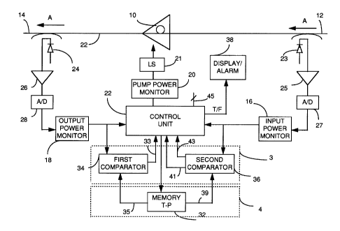
The block diagram of an unidirectional/uni-channel optical
amplifier module equipped with a failure detection system is
illustrated in Figure 1A. The optical amplifier module comprises an
optical amplifier 10, which in the example of Figure 1A is an Erbium
doped fiber amplifier (EDFA). The amplifier module is connected into
optical fiber 22 for amplifying an incoming optical signal received at
input port 12 to obtain an outgoing optical signal at output port 14. The
EDFA module conventionally comprises an input power monitor 16,
an output power monitor 18 and a pump power monitor 20. The
output power monitor 18 receives a fraction of the outgoing optical
CA 02172873 2001-03-19
7
signal after it was converted to an output electrical signal, and measures the
power in the outgoing optical signal. This feedback power information is
processed by a control unit 22 which also controls the pump power monitor 20
for adjusting the power of the laser pump 21 according to the feedback signal.
The input power monitor 16 measures the power of the incoming optical signal,
which measurement is then used for determining various parameters of the
amplifier. For example, the input power may be used to obtain noise
information,
as disclosed in the aforementioned U.S. Patent Application, No. 08/261,350,
now
Patent No. 5,513,029 issued April 30, 1996. Control unit 22 exchanges
information with a remote or local computer along data bus 45.
An input and output tap are conventionally used at input and output ports
12 and 14 to divert a fraction of the incoming and outgoing optical signals to
the
respective power monitor. The respective tapped fraction is converted to an
electrical signal by PIN diodes 23, 24, then amplified by transimpedance
amplifiers 25, 26 and converted to a digital signal by analog to digital
converters
27, 28. This method of measuring the power of optical incoming and outgoing
signals is known in the art and therefore further details are not provided
here.
Generally, an optical amplifier module is provided with an alarm that
declares a LOS when the input signal is less than a threshold level. If an
optical
amplifier is unable to obtain its provisioned output power such as determined
by
the output power control loop while the pump laser is driven to its limit, an
internal alarm state is declared. This is not sufficient, as there are various
reasons why the output power may not be obtained and, accordingly, various
ways of correcting this situation or declaring an appropriate alarm.
According to this invention, the optical amplifier module is epuipped with a
failure detection system comprising means for measuring a performance
parameter of the module, means for providing an expected performance
parameter; and means for comparing the measured performance parameter with
the expected performance parameter, to provide an error signal. The error
signal triggers appropriate alarms; a display of the type of error may also be
provided.
21'~2~73
8
In the embodiment of Figure lA, the performance parameter is
preferably a correspondence between the output and input powers for a
transmission channel. The input power monitor 16 provides a
measured input value (I) on line 37 as a function of the power of the
optical incoming signal, and the output power monitor 18 provides the
measured output value (O) on line 31 as a function of the power of the
outgoing optical signal. The expected performance parameter is a
provisioned output power (P) corresponding to a threshold value (T)
for the input (I) necessary to obtain the respective output (O).
IO Preferably, the means for providing 4 is a memory 32 which stores a
correspondence between (P) and (T). Memory 32 could be a non-
volatile type of memory, in which case the expected parameters) may
be stored by the manufacturer, and cannot be modified by the user.
The means for comparing 3 comprises a first comparator 34 for
comparing the measured output value (O) with the provisioned value
(P) received on line 35 and producing an error signal 33, indicating that
the amplifier output is less than the provisioned value. This may be
part of the output power control loop.
Before declaring a module failure, the system determines if
sufficient input power is provided for obtaining the provisioned
output power, independent of the LOS thresholds that may have been
provided. Thus, if signal 33 indicates that the output power is too low,
a second comparator 36 compares the measured input value (I) with
the threshold input value (T) retrieved from memory 32 on line 39. If
the measured input value (I) is below the threshold, then an "Input
Low" alarm 41 is generated, indicating that the user is expecting too
much gain from the amplifier. This would be caused by the input
power being too low, or the provisioned output power being too high.
If the input power is above the threshold, then a"Unit Fail" alarm 43 is
generated, indicating that the amplifier is not functioning to its
guaranteed performance level.
The failure detection system is also provided with a
display/alarm unit 38 for indicating a failure of the module when (O) is
less than (P) and also for indicating if it is a module failure or an input
low situation.
It is to be understood that control unit 22 exchanges control
signals with the input power monitors 16 and 18, comparators 34 and
21'~287~
" 9
36 and memory 32. These signals are not illustrated for brevity of the
drawings.
Figure 1B illustrates the method for determining failure of an
unidirectional/uni-channel amplifier module. During the
initialization step 100 the provisioned output (P) and the
corresponding threshold value (T) are stored in memory 32. The
correspondence can also be a table giving a plurality of expected power
values, each paired with a corresponding threshold for the input. The
power of the output signal is measured in step 110 to give the
measured output value (O). Next, in step 120, the provisioned power
(P) is retrieved from memory 32 and compared with the measured
output value (O) in comparator 34. If output value (O) is greater or
equal to the provisioned value (P), steps 110 and 120 are repeated, as the
module functions according to the provisioned parameter.
If signal 33 is false, the measured input value (I) is determined by
the input power monitor 16 in step 130. In step 140 the threshold value
(T) is retrieved from memory 32 and compared with the measured
input value (I) in the second comparator 36. If comparator 36 issues
control signal 41, control unit 22 determines that in this case the
incoming optical signal is too low, or the provisioned power is to high
and block 38 will display the appropriate indication in step 150. If
comparator 36 issues control signal 43, the control unit 22 interprets it
as a module failure and accordingly instructs alarm block 38 to trigger
the appropriate alarm in step 160.
In a bidirectional optical amplifier, or in a mufti-channel
amplifier, the above method can be applied separately for each
direction/channel. Figure 2A illustrates a case when this method is
applied to a bidirectional amplifier module using a combined
performance parameter. The amplifier module of Figure 2A is
provided with separate power monitors and laser sources for each
direction. Figure 2A illustrates one block 16 for both input power
monitors, one block 18 for the output power monitors, one block for
the pump monitors and one laser source block, for simplification.
The incoming optical signal for a first direction A, illustrated in
this Figure from right to left, is tapped at input port 12, converted to an
electrical analog signal by the PIN diode 23 and transimpedance
amplifier 25, converted then to a digital signal by analog to digital
~1'~~~'~3
converter 27; and applied to the input power monitor unit 16 to
produce the measured input value (I1). The outgoing optical signal for
the first direction A gives the first measured output value (01) along
the path made of PIN diode 24, transimpedance amplifier 26, analog to
5 digital converter 28 and output power monitor unit 18.
The incoming and outgoing optical signals for the second
direction of transmission (or the second channel) B, illustrated in
Figure 2A from left to right, are also measured. A second measured
input value (I2) is obtained along the path made of PIN diode 13,
10 transimpedance amplifier 15, analog to digital converter 19 and input
power monitor unit 16. The corresponding measured output value
(02) is obtained along the path made by the PIN diode Z4,
transimpedance amplifier 16, analog to digital converter 17 and output
power monitor unit 18. The control unit 22 receives the information
regarding the power of the incoming and outgoing optical signals and
controls each pump power monitor 20 for setting the power of laser
sources 21 to obtain the desired amplification for the respective
direction (channel). Other parameters of the module are monitored by
the control unit. As in the embodiment of Figure lA, control unit 22
exchanges information with a computer on data bus 45.
The first and second output values (01) and (02) are applied to a
first calculation arrangement 40 which calculates a combined
measured output signal F(O) on line 45 which is a function F(01, 02).
A second calculation arrangement 42 receives the measured input
values (I1) and (I2) and calculates a combined measured input signal J(I)
on line 47, as a function J(I1,I2).
Memory 32 stores a direct correspondence between the
provisioned combined output F(P), which is the same function F of the
provisioned output powers for the two directions (channels), and a
combined threshold J(T), which is the same function J of the thresholds
for the two directions (channels).
The first comparator block 34 receives the measured and
provisioned combined outputs and produces the error signal 33
indicating that the output power is too low, as disclosed above in
connection with Figures lA and 1B.' If F(01,02) is less than F(P), the
second comparator 36 compares the combined measured input J(I1,I2)
with the combined threshold J(T). If the combined measured input is
21'~?~'~3
11
greater than the combined threshold J(T), then the "Unit Fail" alarm
43 is generated and display/alarm unit 38 indicates that the amplifier is
not functioning to its guaranteed performance level. If the combined
measured input value is below the threshold, then the "Input Low"
alarm 41 is generated and display/alarm unit 38 indicates that the user
is expecting too much gain from the amplifier.
Figure 2B illustrates the flow chart for the operation of a failure
detection system for a mufti-channel optical amplifier module as
illustrated in Figure 2A for two channels. Functions F and J are
selected in step 200, and in step 210 the correspondence between the
calculated combined provisioned output power F(P) and the combined
threshold J(T) is stored in memory 32. Next, in step 220, fractions of the
outgoing optical signals for all M transmission channels are diverted to
the output power monitor block 18 and processed to determine the
output values 01, 02~ "Om,.. OM. Function F(01, 02,..Om,..OM) is
calculated in the first calculation arrangement block 40 in step 230 for
obtaining the combined measured output power F(O). For two
transmission channels as shown in Figure 2A, the calculation
arrangement 40 determines the function F(01, 02).
If in step 240 it is determined that the combined measured
output F(O) is equal or greater than the combined provisioned output
power F(P) retrieved from the memory, the module functions within
the provisioned parameters and steps 220, 230 and 240 are repeated for
continuous monitoring of failures. If it is determined that the
combined measured output F(O) is smaller than the combined
provisioned output F(P), the system checks if the input power is
sufficient for obtaining the provisioned output power. The measured
input values are provided by the input power monitor 16 in step 250.
The measured input values are applied to the second calculation
arrangement 42 where the function J(I1,I2,..Im,..IM,) is calculated to
provide the combined measured input value J(I) in step 260. For the
case when the transmission system has two transmission channels as
shown in Figure 2B, the second calculation arrangement block 44
calculates function J(I1,I2).
Next, in step 270, J(T) is retrieved from memory 32 and
compared with J(I) to verify if the incoming signal is above a threshold
for obtaining the provisioned power for the outgoing signal. If J(I) is
CA 02172873 2001-03-19
12
smaller than J(T), the system informs the user that the input power is too
low, or
that the provisioned power is too high, as illustrated in step 280. Block 36
generates signal 41 and the control unit 22 displays the appropriate
information
on the alarm/display block 38. On the other hand, if J(I) is greater or equal
to
J(T), the control unit 22 triggers alarm block 38 to inform the user of a
module
failure in step 290.
Functions F and J may be the sum of the two input or output values.
Other mathematical functions such as maximum can also be used in place of the
sum. Hysterisis of, for example, 1 dB can be implemented to prevent excessive
toggling of alarm states. Interpolation can be used to provide better
resolution
than that chosen for the table step-size, which could be, for example, 2 dB. A
polynomial fit or other method of data reduction can be used instead of a
table to
require less storage at the cost of more processing. As well, it is possible
to
store in memory 32 a table with provisioned outputs for the inputs for each
channel and have the calculation arrangement to determine functions F(P) and
J(I) according to the number of channels in actual use. The preferred
embodiment depends on the application.
Figures 3 and 4A illustrate a failure detection system for an optical
amplifier module as described next.
Input and output signal powers are measured and signal wavelengths
recognized for example by the method disclosed in U.S. Patent Application No.
08/261,350, now Patent No. 5,513,029 issued April 30, 1996 (Roberts et al.).
These power values are converted by control unit 22 to photon flowrate values
FSIG11 to FSIGIM and FSIG01 to FSIGOM for the input and output signals at
wavelengths ~.1 to ~,,yl respectively. Similarly, amplified spontaneous
emission
(ASE) power values, measured by any suitable method as disclosed, for
example, in the above-identified U.S. patent application, are converted by the
control unit to flowrates FASEin and FASEout. In addition, the pump back facet
monitor current value (L) is converted by control unit 22 into a pump photon
flowrate value FPUMPin.
All above conversion factors are worst case values, common to all
amplifier units and obtained from a prior knowledge of the amplifier design.
Using flowrates obtained at start of life, slowly varying monotonic functions
FOM1 are evaluated and stored in non-volatile flash memory 32 accompanying
each amplifier unit. In particular:
21'~2~73
''~ I3
M
FPUMPin + 2 - (FASEZn - FASE°u~ ~+ ~ (FSIGln - FSIGOn )
FOMl = M n (EQ1)
~FSIGln +FPUMPIn +FASEIn
n
This expected figure of merit can be determined in the factory,
once the amplifier has passed detailed optical tests, and then the figure
of merit and some of the test results can be stored in the non-volatile
memory 32 of each amplifier. The figure of merit can be reported to the
user or to a factory repair person. Pass/fail criteria applied to the
function FOM1 evaluated at start of life (t=0), can be used to identify
modules suspected of unacceptable pump performance or to determine
modules with unacceptable performance.
An error signal obtained from the difference between start of life
values, FOM1 t=~ , and corresponding values measured during the "in
service lifetime" of the amplifier, FOM2 t=t, can be used to measure
deterioration in pump laser efficiency. In particular:
epump=FOMlr-° - FOMlt-t (EQ2)
To this end, the current figure of merit is compared in
comparator 34 with the provisioned (start) value retrieved from
memory 32. Pump efficiency deterioration is measured as an increase
in the value of epump. Alarms can be derived using this error signal.
As well, epump could be evaluated for a particular channel n, or could
be a combination of n values.
Pump efficiency can deteriorate due to such things as a change in
pump wavelength, change in optical path or alignments, and
component losses. If the optical performance of the amplifier is
degraded, such as by increased internal losses, changes in coupling, or
changes in pump wavelength, then this figure of merit will be reduced,
namely the measured FOM will be smaller than the provisioned value.
In this case, error signal 33 informs the control unit 22, which in turn
triggers the appropriate alarm, and/or displays a corresponding
message.
2~'~2~'~3
'' 14
Figure 4A illustrates the flow-chart for the operation of the
failure detection system of Figure 3. In step 300, the definition of the
figure of merit FOM1 is established, and in steps 310 and 320 the
expected FOMI t=~, which is the start value, is determined and stored in
memory 32. In step 330, the input and output powers are measured
together with the ASE power value. The values FSIGIn and FSIGOn
are determined by the control unit 22 from these measurements. The
current FOM1 is calculated in block 44 in step 340 and compared in step
350 with the start value FOMlt=~ in comparator 34 to generate the
epump signal 33. If the expected FOMlt=a is smaller than the
measured value, the control unit 22 triggers alarm block 38 to indicate
and display that the module has degraded its performance and service
or replacements are necessary.
Another parameter that may be measured for determining the
performance of an optical amplifier module is the amplified
spontaneous emission (ASE). The basic embodiment for detecting a
module failure based on this parameter is illustrated in Figure 3.
Figure 4B shows the block diagram for the operation of this
embodiment.
The expected amount of ASE can be calculated in a calculation
unit 44 using the input power and the pump power from the input
power monitor 16 and the pump power monitor 20. A function
FOM2 n determines the effective input loss of the optical amplifier, or,
equivalently, the amount of amplified spontaneous emission.
Knowing the effective input loss is equivalent to knowing the amount
of amplified spontaneous emission for a given amplifier design
because the effective input loss adds directly to the noise figure of the
amplifier. In particular:
FOM2n = ~FASEout - FASEin) ~ FSIGIn (EQ3)
FSIGOn
FOM2n is evaluated at start of life and stored in non volatile
flash memory 32. Higher values of FOM2 correspond to a higher input
loss for a given amplifier design.
The error signal 33 output by comparator 34 is obtained from the
difference between start of life values, FOM2nt=0 and corresponding
~1'~2~73
'~ 15
values measured during the amplifier's in-service lifetime, FOM2y~t=t ,
Error signal 33 can be used to measure deterioration in input loss. In
particular:
elosS = FOM2t-t . FSIGOn _FOM2t-~ . FSIGOn (EQ4)
FSIGIn n FSIGIn
Input loss deterioration is measured as an increase in the value
of elossn. Alarms can be derived from signal 33 evaluated at a
particular n or a combination of n values.
Figure 4B illustrates the block diagram for the operation of the
embodiment of Figure 4A. First, in step 400, function FOM2 is selected
and the start values FOM2t=~ (at t=0) are determined in step 420. This
value is determined using input (I) from input power monitor 16, the
value of the output ASE from the output power monitor 28, and the
value of the input ASE from the pump power monitor 20. In step 420
the start values are stored in memory 32. Next, in step 430, the module
measures the input (I), output (O) and pump (L) powers, and
calculation unit 44 determines in step 440 the current value for FOM2 y~.
The measured value of the figure of merit at time t is compared with
the start value in step 450 in comparator 34 to produce the error signal
33 for the control unit 22. If signal 33 indicates that the current figure of
merit FOM2n is smaller or equal to the start value FOM2nt=0, steps 430
to 450 are repeated, in that the amplifier functions within the
provisioned parameters. When the noise becomes greater than the
expected ASE, failure of the module is declared by the alarm/display
unit 38 in step 460.
The gain tilt may also be used as the parameter of the amplifier
for measuring its performance, as shown in the embodiment of Figure
5A. The preferred implementation of the gain tilt calculation is
described in the following.
There is a predetermined set of wavelengths at which a given
amplifier unit operates, namely wavelengths ~,1 to ~,M. The gains Gl to
GM (decibels) at each of the wavelengths ~,1 to ~,M are measured in the
factory under a nominal gain condition of, for example, 23 dB at
1557nm. The gains are then saved in non-volatile flash memory 32 on
that amplifier module.
- 16
When the amplifier inversion condition changes away from
nominal due to a change in the input powers or in the pump powers
provided, the gains at each wavelength change in different, but
predictable relative amounts. For a given amplifier design, there is a
fixed set of tilt coefficients C1 to CM (decibels/decibel) that define the
normal relative changes in gain. These coefficients are also saved in
the flash memory 32 within each amplifier module, so that they can be
used to distinguish normal gain changes from abnormal ripple. In
addition, a given error threshold (T) provided by the manufacturer is
also stored in memory 32.
The gain tilt error is calculated as follows:
em= (gm-Gm) - (gn-Gn) X (Cm/Cn) (EQ5)
where m is an integer, m E ~1, M~ and where: n is the smallest
wavelength number of those present; gm is the present gain for
channel (m); and Gm is the expected gain for channel (m).
Figure 5A illustrates a block diagram of an embodiment for
determining a failure of the amplifier using the gain tilt error
calculated according to relation EQS. Periodically, or on request while
in operation, the current gains g1 to gM being provided by the amplifier
are measured with gain detector 50 for the wavelengths that are
present. Then, the system determines which is the smallest
wavelength number of those present, using a minimum detector 48.
The number of this channel is denoted by "n" and the channel for
which the measurements are performed is denoted by "m". The
expected gain of (n) channel Gn is retrieved from memory 32 on line
49, together with the respective gain tilt coefficients Cn and Cm, and
applied to a first calculation arrangement 44. Then the first term (gn-
Gn)Cm/Cn is determined by unit 44. At the same time, a second
calculation arrangement 46 receives from memory 32 the expected gain
Gm for the channel under consideration and receives from the control
unit the measured gain gm. The second calculation arrangement
determines the second term (gm-Gm). The first and second terms are
applied on lines 47 and 51, respectively, to comparator 34.
If any error, or a function of the errors such as the sum of the
absolute values is beyond the threshold (T) received on line 55, then
17
the error signal 33 will trigger a gain ripple alarm. This alarm indicates
that the ripple in the gain of that amplifier is excessive due to a failure
in a component such as an optical filter and that the amplifier needs to
be replaced.
An improvement of this method is to use a least squares best fit
profile to determine a performance parameter go for gain, rather than
using one of the signal gains gn. The best fit calculation is the well
known minimization of the sum of the squares of the errors. This
implementation is more tolerant to gain measurement errors by being
a best fit to a plurality of measurements, rather than being leveraged
from a single point. Wavelength zero could be selected, for example, as
an arbitrary reference point such as 1545 nm that is not a signal
wavelength. Co is set to 1.0 by scaling the array. The error equation
then becomes:
em = (gm -Gm - (go -Go ) X Cm (EQ6)
Figure 5B shows the operation of this embodiment. In step 500
the gains G1 to GM for each wavelength are determined for the
respective module at a nominal gain condition of 23 dB at 1557 nm, for
example. The gains are then saved in non-volatile flash memory 32 in
step 510 as the expected performance parameter. Tilt coefficients C1 to
CM that define the normal relative changes in gain are also stored,
together with an admissible error threshold. In step 520, the input,
output and pump powers are measured and the current gains gl to gM
are determined therefrom, also using the gain tilt coefficients. The
error is calculated in step 530 according to EQ5 or EQ6, for example. If
the error is beyond the threshold as determined in step 540, the control
unit 22 declares a fault in the module and triggers the alarm block 38 in
step 550.
Another performance parameter for obtaining information
about functioning of a multiband amplifier is the control dynamic
range. The embodiment that is used for such a measurement is
illustrated in Figure 6A for a two band amplifier and the mode of
operation is illustrated in Figure 6B, for a multiband amplifier.
If an optical amplifier with two bands, having somewhat
independent power control, is unable to simultaneously obtain its
18
provisioned output powers in both of its bands due to the control
running out of dynamic range, the failure detection system compares
first the two measured output values representative of the output
power with the two provisioned output powers. The non-volatile
memory 32 contains a three dimensional table that has dimensions of
the first provisioned output power Pl, the second provisioned output
power P2~ and the first input values Il. The records in each location of
the table are the maximum and the minimum powers for the second
input I2, namely I2Min and I2Max, under those conditions.
An example of a table is given in the following, with only two
values for Il shown for brevity:
TABLE
POUT1 +3 +6 +9 +12
POUT2 I2 (Max/Min)I2 (Max/Min)I2 (Max/Min)I2 (Max/Min)
+3 -7/3 -6/6 -5/7 -5/9
I1 = +6 -6/3 -5/6 -4/8 -4/9
0 dB +9 -5/3 -4/6 -4/9 -3/11
+12 -4/3 -3/6 -3/9 -2/12
+3 -23 /-10 -24 / 17 -24 /-14 -27/-16
I1= +6 -20/-5 -20/-8 -20/-9 -23/-10
-15 dB +9 -16/0 -15/0 -16/-5 -18/0
+12 -10/0 -9/+1 -9/+3 -8/+5
The system measures the output power for the first and second
transmission channels and provides the measured output values Ol
and 02. A first comparator 34 receives on its inputs the measured
output values 01 and 02 and compares them with the provisioned
values Pl and P2 received from memory 32 on line 35.
If the output powers are out of the designed range for that
amplifier, the first comparator 34 will issue the error signal 33 to the
control unit 22 for initiating the verification of the inputs. The input
power is then measured for the first and second channels to give the
measured input values Il and I2. The range I2Min-I2Max,
corresponding to values Il, Ol, and 02 is retrieved from the table stored
in memory 32. This record is input to a second comparator 36. Second
comparator 36 also receives the measured input value I2 from the
2~7~~73
w 19
second input power monitor and compares it with I2Min and I2Max~ If
the power measured on the second input is within the range tabulated,
then the amplifier is declared failed, with signal 41 indicating that the
amplifier module is not functioning to its guaranteed performance
level. If the power measured is outside the tabulated range, then a
"control dynamic range" alarm is declared by the control unit on
receipt of signal 43.
Hysterisis of, for example, 1 dB can be implemented to prevent
excessive toggling of alarm states. Three dimensional interpolation
can be used to provide better resolution than that chosen for the table
step-size, which could be, for example, 2 dB. Polynomial fits or other
methods of data reduction can be used instead of tables to require less
storage at the cost of more processing.
With an amplifier having M bands, this method can be
generalized by using a table of dimension 2*M-1. In this case, one of
the inputs, which we will note as input I1, has its range tabulated as a
function of all of the others. As shown in Figure 6B at step 600, the
table TAB2M-1 is stored in memory 32. The table has records of the
form IlMin-IlMax~ In step 610, the output power monitors are
instructed by the control unit 22 to provide the measured output
values for all M transmission channels. Next, in step 620, the
measured output values are compared to the provisioned powers in
the first comparator 34 to obtain the error signal 33. If the output
powers are in the provisioned range for all outputs, steps 610 and 620 ,
are repeated. If signal 33 is false, then the inputs are measured in step
630 to obtain the measured input values I1, .. IM for all channels. In
step 640 the memory is accessed and the record IlMin-IlMax
corresponding to the measured 01, ..OM, I2, ..IM is retrieved from the
table TAB2M-1. In step 650 comparator 36 determines if the measured
input value I1 is in the range IlMin - IlMax~ If I1 is within the range,
the module is declared failed, as shown in step 660. If the input is
outside the range, the appropriate alarm is displayed in step 670.
In some cases this may not give a sufficient observation of the
space of valid operation, and several such tables would be consulted,
with different choices of variables. In other cases the tables can be of
reduced dimension and several variables tabulated. These cases are
~1'~2~'~3
determined by the control specifics of the particular amplifier and the
accuracy desired.
Still another performance parameter for determining the failure
of an amplifier module is the output loss. The output loss can be
5 calculated in a manner similar to the above methods, using the gain
values. According to this method, the gains g1 and g2 of the module at
two wavelengths ~,1 and ~,2 are selected from the measured gains so as
to have the greatest difference between the respective gain tilt
coefficients Cl-C2 , for best accuracy. The average inversion is then
10 determined according to the following relationship:
INV2 = (g1- g2 ~ ' a + l~ (EQ~)
Cl _ C2
where a, (3 are constants for a given amplifier design.
I5 The expected additive ASE photon flux can be calculated by:
FASE~aIc =(eA~INVz -1~. y (EQs)
where A and y are constants for a given design.
20 The output loss is equal to the ratio:
outputloss = FASEcatc (EQ9)
FASEout - FASEin
Figure 7A shows a block diagram for a failure detection system
using this parameter. The calibrated gain tilt coefficients C1 to CM for
all M transmission channels are determined at the factory and stored in
memory 32. At predetermined intervals, the maximum detector 48
determines which transmission channels are active and determines
channels "n" and "m" with the highest difference between the gain tilt
coefficients. The current gains gn and gm being provided by the
amplifier are measured for ~,n and ~,m in gain detector unit 50. A first
calculation arrangement 44 receives the gain tilt coefficients Cn and Cm
for these channels and the measured gn and gm and calculates
FASEcalc~ A second calculation arrangement 46 receives FASEcalc and
21'~~8'~~
- 21
also the measured FASEin and FASEout and calculates signal output
loss according to EQ9..
The output loss is compared to a calibration value of output loss
that is stored in the non-volatile flash memory 32 at the factory and an
output loss alarm is declared if the difference is beyond a given
threshold.
Figure 7B illustrates a flow chart of the operations executed by
the system for detecting failure of the amplifier module according to
the embodiment of Figure 7A. In step 700, the calibrated C1 to CM and
the calibration value T for the output loss are stored in memory 32.
Detector 48 determines, out of all active transmission channels, the
channels (n) and (m) presenting a maximum difference between the
gain tilt coefficients in step 710. Next, FASEcalc is calculated in the first
calculation arrangement 44 for the channels selected by detector 48. In
step 730, the ASE for the input and output are measured by the
amplifier module and these values are used to calculate the output loss
in step 740. Next, the output loss is compared with the calibration
value T in step 750 and the alarm block 38 is triggered in step 760 by the
error signal when the output loss is higher than the calibration value.
Furthermore, a model of the amplifier can be computed within
the microprocessor and the performance of that amplifier compared to
the model results. This can be made computationally efficient by
condensing the amplifier model to a set of polynomials. The amplifier
parameters could be transmitted to a separate or central computer and
the evaluation of those parameters calculated there. The amplifier
module may be provided with some or all the above disclosed
embodiments, by addition of a minimal number of components and
software.
While the invention has been described with reference to
particular example embodiments, further modifications and
improvements which will occur to those skilled in the art may be made
within the purview of the appended claims, without departing from
the scope of the invention in its broader aspect.