Note: Descriptions are shown in the official language in which they were submitted.
212888
PLANAR DIELECTRIC LINE AND
INTEGRATED CIRCUIT USING THE SAME
The present invention relates to a planar
dielectric line for use in a microwave or millimeter-wave
band. The invention also relates to an integrated
circuit using the dielectric line.
Microwaves and millimeter-waves, which are
electromagnetic waves in a very wide range of from 300
MHz to 300 GHz, are used in various types of radar,
long-distance telephone networks, television broadcasting
relays, satellite communications, etc. such waves are
also coming into wide use in the field of mobile
communications. Meanwhile, research is being actively
conducted for the development of MMICs, and progress is
being made in the downsizing of equipment utilizing
electromagnetic waves in the range of microwaves and
millimeter-waves. Accordingly, microwaves and
millimeter-waves are increasingly coming into a wider
range of uses.
Hitherto, several types of transmission lines
have been largely used in the range of microwave and
millimeter-waves, such as waveguides, coaxial lines,
microstrip lines, coplanar lines, slotted lines, and so
on. These transmission lines are constructed by forming
predetermined electrodes on a dielectric substrate.
Waveguides are for use in applications where conductor
losses should be inhibited to a low level. Coaxial lines
are widely used as connecting cables between equipment.
Coplanar lines, microstrip lines, slotted lines, etc. are
largely employed for forming connections between
electronic parts, such as ICs, since they are easily
connected thereto.
_ X172888
- - 2 -
A slotted line is, as shown in Fig. 19,
constructed in such a manner that electrodes 421a and
421b are disposed across a predetermined spacing on the
top surface of a dielectric substrate 423 having a
predetermined thickness h400. This achieves the
formation of a slot 424 having a predetermined width W400
sandwiched between the electrodes 421a and 421b. In the
slotted line constructed as described above, an
electromagnetic wave forms a mode having an electric
field E400 in parallel to the width of the slot 424 and a
magnetic field H4oo in parallel to the longitudinal
direction of the slot 424, thereby propagating in the
longitudinal direction of the slot 424.
Further, in addition to the above-described
transmission lines, nonradiative dielectric waveguides
(NRD) are used. An NRD is constructed by interposing a
square-prism-shaped dielectric member between conductive
plates, and causes only a low level of conductor losses.
The transmission lines mentioned above have
various disadvantages in the microwave and millimeter-
wave bands. Waveguides, which are of large size, cannot
achieve downsizing and weight reduction and are difficult
to connect with electronic parts, such as ICs. In
coaxial lines, an unnecessary high-order mode is
generated at a frequency higher than a specific frequency
determined by the cross sectional configuration of the
coaxial lines so as to increase conductor losses, thus
rendering the lines inoperable. In order to avoid this
problem, it is necessary to reduce the diameter of the
coaxial line to approximately 1 mm when the line is used
at a frequency in a millimeter-wave band as high as 60
GHz, which makes it difficult to manufacture. Microstrip
lines, coplanar lines and slotted lines exhibit extremely
CA 02172888 2002-08-13
large conductor losses. Additionally, NRD lines are
difficult to connect to electronic parts, such as ICs.
Accordingly, in order to overcome the above-
described drawbacks, it is an obj,:ect <:~f an a;>pec:t of the
present invention to provide a small and inexpensive
planar dielectric line in which easie connection with
electronic parts, such a~. ICs and she like, can be
achieved and conductor losses can be inhibited to a much
lower level than those of conventi.onaL microstrip lines,
coplanar lines, slotted lines and ~~o <>n.
It is another object of an aspect of the
present invention to pz:~oiJide an iml~egr_~ated circuit with
comparatively improved compactnesv and strength.
In order to achieve the above objects,
according to a first aspect of t:he~ pre-'sent: invention,
there is provided a planar dielectric line comprising: a
dielectric sub:~trate having first and second surfaces
which opposedly face each other; <~ first slot having a
predetermined width and being interpo:~ed between first
and second electrodes, the fir:~t: and :second electrodes
being formed on the first surface o.f the dielectric
substrate and opposedly facing eacLi other across a
predetermined spacing; and a. secorlc:~ s:l of having
substantially the same width as the first slot and being
interposed between third and. fc.~urt::h e:l.ectr~odes, opposedly
facing the fi_Nst slot, the third and f:ourth electrodes
being formed on the second surface of the dielectric
substrate and opposedly .facing each other across a
predetermined spacing, wherein they diE.lectric constant
and the thickness of: the dielectric-_~. substrate are
determined so that a plan=_ e:l.e<:~trcarnagrnetic wave having a
predetermined frequency and propagating in. a propagation
region of the dielectric substrate interposed between the
2I72888
- - 4 -
first and second slots is totally reflected by the first
and second surfaces of the dielectric substrate adjacent
to the first and second slots, respectively.
According to a second aspect of the present
invention, there is provided a planar dielectric line,
further comprising a first conductive plate disposed away
from the first surface of the dielectric substrate across
a predetermined distance, and a second conductive plate
disposed away from the second surface of the dielectric
substrate across a predetermined distance.
According to a third aspect of the present
invention, there is provided a planar dielectric line,
wherein a dielectric is disposed between the first
surface of the dielectric substrate and the first
conductive plate and between the second surface of the
dielectric substrate and the second conductive plate, the
dielectric having a lower dielectric constant than that
of the dielectric substrate.
According to a fourth aspect of the present
invention, there is provided an integrated circuit
comprising a transmission line and a high-frequency
device connected to the transmission line, wherein the
transmission line includes at least one of the planar
dielectric lines of the types described above.
In the planar dielectric line according to the
first aspect of the present invention, in the propagation
region of the dielectric substrate, an electromagnetic
wave having a frequency higher than a predetermined
frequency is totally reflected by the first surface of
the substrate adjacent to the first slot and by the
second surface of the substrate near the second slot. On
the other hand, the portions of the substrate other than
the propagation region, interposed between the first and
~I72888
- 5 -
second electrodes, attenuate the plane electromagnetic
wave. Accordingly, a high-frequency signal having a
frequency higher than a predetermined frequency is
propagated in the dielectric line while concentrating
inside and in the vicinity of the propagation region.
The planar dielectric line according to the
second aspect of the present invention is constructed by
adding the additional first and second conductive plates
to the dielectric line implemented by the first aspect of
the present invention. This forms a cut-off region
between the first electrode and the first conductive
plate and also a cut-off region between the second
electrode and the first conductive plate, the plane
electromagnetic wave being attenuated in both the cut-off
regions. A further cut-off region is formed between the
third electrode and the second conductive plate so as to
attenuate the plane electromagnetic wave. Another
cut-off region is also formed between the fourth
electrode and the second conductive plate so as to
attenuate the plane electromagnetic wave. This further
prevents leakage to the exterior of high-frequency
signals propagating in the above-described planar
dielectric line and also precludes the unnecessary entry
of high-frequency signals from the exterior of the
dielectric line.
In the planar dielectric line according to the
third aspect of the present invention, the following
features are added to the dielectric line according to
the second aspect of the present invention. Namely, a
dielectric is interposed between the first surface of the
dielectric substrate and the first conductive plate, and
another dielectric is also interposed between the second
surface of the substrate and the second conductive plate,
CA 02172888 2002-08-13
G
each dielectric having a lower dielectric constant than
that of the dielectric :m.~bst~rat.e . ~I'hi.:~ makes i_t possible
to decrease a spacing bet ween the f i.r~t surf ace of the
substrate and the first conductive plate and also a
spacing between the sec:orvd surface: of the substrate and
the second conductive plate, thus making the overall
planar dielectric line thinner.
The integrated cix~cu it. a~~~cox-ding to the fourth
aspect of the present i.nvent:iorz c:->mpr i_ses a transmission
line and a high-frequency device connected to the
transmission line. The t:xansmi~si~:or1 l i_ne includes at
least one of the dielec:t:ric 1_ines ~_>f t::he types described
above.
According to an aspect of the present invention
there is provided a planar dielectric line comprising:
a dielectric substrate having first and second
surfaces which opposed:l..y face each ot=her;
a first s:Lot. having a predetermined width and
being interposed between first and second electrodes,
said first and SP_COT'ld electrodes l:>eing formed on the
first surface o.f said dielectric .>an:b:;t rate anal opposedly
facing each other across a predetermined spacing; and
a second Mot having sub:».arut~ial_ly the same
width as said first slat and being interposed between
third and fourth electrodes, opposedly facing said first
slot, said third and fourth electz ~_,de~ bei_ng formed on
the second su:rf.ace of ;;aid die Lect: r.ic: substrate and
opposedly facing each other across a predetermined
spacing;
wherein the permitt.ivi.ty and the thickness of
said dielectr=is substrate are deter-mined so that said
planar dielectric line co.nfine:~ about 80 percent or more
of energy of: a signal propagating in .paid dielectric
substrate between said first and sf~clOrld slots and meets
CA 02172888 2002-08-13
6a
the following conditions:
relative permi.tti.vity of dielectric substrate
>-10 thickness "t" ot_ ~:~:iW! ec:tr is ='e~; . 3 rnm;
and further comprising:
first and second conductive substrates, and
first and second air layE~rs defined re=spectively between
said first and second conductive substrates, and said
first and second surfaces of sa=id diel..ectric substrate;
wherein the t:hickness "t" of said dielectric
substrate and the thic=kness "a" of eac=h said air layer
are determined to meet the following c::onditions:
t~~,g/2 ~,g . wavelength in dielectric substrate
a'7~"/2. 7~0 : f::r_ee space waveleyngth.
According to another aspect of the present
invention, there is provided a planar dielectric line
comprising:
a dielectric substrate having first and second
surfaces wh:ic.h opposed:Ly face eacr-c ot~uer;
a first slot having a predetaermined width and
being interposed between first and sec:;vond electrodes,
said first and second electrodes L~ein<~ formed. on the
first surface of said dielectric :a~..~bst~rate and opposedly
facing each other across a predet:e~:r_~rnirued spacing; and
a second slot: having substantially the same
width as said f=irst slot and bc~i.nc:~ inl:::erposed between
third and fourth electrodes, opposedly facing said first
slot, said t=h=ird and fourth electoa:>de.=~ being formed on
the second surface of said dielectric substrate and
opposedly facing each other across:~ a ~>redetermined
spacing, wherein thE~ pE-~.rmittiv~_ty ~~nd the thickness of
said dielectric substrate are determirned t.o meet the
following conditions:
relative permittivity of dielectric substrate
~18 t~'ll CkrlE~t:s "t" Of l:l.~:? L ?O't: C' 1 ~~' ::>1.1~7St..I cdtE: .'0 .
3 mIrl.
CA 02172888 2002-08-13
6b
According to another aspect of the present
invention, there is provided an ir~t:egrated circuit
comprising a plurality of: planar cxielf~ctric 7.ines each of
which comprises:
a dielectric sl.ibstrate lnavirng first and second
surfaces which opposedl.y face each other;
a first slot having a predetermined width and
being interposed between first anc3 second electrodes,
said first and second electrodes bein<~ formed on the
first surface of said dielectric substrate arid opposedly
facing each other acro,<<~s a prr~detEerm:ilied spacing; and
a second slot having substantia~ly the same
width as said first slot and bein~_~ interposed between
third and fourth electrodes, c>ppose=_d1y facing said first
slot, said third and fourth electrodes being formed on
the second surface c~f said dielecr_:ric substrate and
opposedly facing each other acros:~, a predetermined
spacing;
wherein the permit:tivity anca, the thickness of
said dielectric substrate a.re det~=ermirled so that said
planar dielectric line confines about 80 percent or more
of energy of a sign<~l propagat=ing :in .>aid dielectric
substrate between said first. and second sI_ots and meets
the following conditions:
relative permitt:ivity o~ diEelect.ric substrate
>-1.0 thickness t of ~::iielect..ri~~ ;~i~iv~~t:~:wte '--0.3 mm;
wherein at least one of said first and second
slots has a narrowed bent portion.
According to yet anotherw aspect of the present
invention, there is provided an irutegrated circuit
comprising a pl.uralp_ty of planar <~iel.e=:ctric lines each of
which comprises
a dielectric substrate having (first and second
CA 02172888 2002-08-13
6 c:
surfaces which opposedly face each other;
a first slot having a predetermined width and
being interposed between first and se<~ond electrodes,
said first and second e1E=:ctrodes k~einc~ foamed on the
first surface of said die~lectri.c s~zbst~rate and opposedly
facing each other across a predet~yrmirled spacing; and
a second slot having substantially the same
width as said first slot and being interposed between
third and fourth electrodes, opposedly facing said first
slot, said third and fouxrth e:Lectrode~ being formed on
the second sur:Eace of said dielect::ric substrate and
opposedly facing each other acros~~ a E>redetermined
spacing;
wherein the permittivity and the thickness of
said dielectric substrate are determined so that said
planar dielectric line cc;nfines about 80 percent or more
of energy of a signal propagat ing :in ::,aid dielectric
substrate between said first. and :~c=cored slot~~ and meets
the following conditions:
relative pei:mittivity of dielectric substrate
>_10 thickness "t" of ti~electr~~ um s~Wst t ate >-0. 3 mrn;
and further c~omprisi.ng f~ rst and second
conductive substrates, and fir;~t a;and ~:aecond air layers
defined respectively between said first and second
conductive substrates, and said f._st and second surfaces
of said dielectric substrate;
wherein the thickness "t." of said dielectric
substrate and the thickness "a" of each said air layer
are determined to meet the fol:Lowv~ng conditions:
t'-7~g/2 ~~g . wavelengt=h in diE-:lectric substrate
a~=~,~/2 7~0 : free space wavelength.
According to a fu:rthf~r a:::~pec:t. of the present
invention, there is px:-ovided an ir~.l::eg~:ated circuit
comprising a plurality of planar d:i.electric lines each of
CA 02172888 2002-08-13
6d
which comprises;
a dielectric substrate leaving first and second
surfaces which opposedly face eaerl other;
a first slot having a predetermined width and
being interposed between first and second electrodes,
said first and second electrodes being formed on the
first surface of said dielectric ;.substrate and opposedly
facing each other across a predetermined spacing; and
a second slot riaving substantially the same
width as said first slot and be:inc~ interposed between
third and fourth electrodes, opposedly facing said first
slot, said third and fourth electrodes being formed on
the second surface of said dielectric substrate and
opposedly facing each otroer across a predetermined
spacing;
wherein the permittivity and the thickness of
said dielectric substrate are determined :~o t.hat said
planar dielectric lane confines about 80 percent or more
of energy of a signal propagating in ;paid dielectric
substrate between said first and :second slots; and
wherein the permit;tivity anti the thickness of
said dielectric substrate a.re determined to meet the
following conditions:
relat:.ive perr~ci.ttivity of dielectric substrate
>18 thickness "t" ol: <~ii.ele~ct..r.i;: s~_uost r at.e ?0. 3 mm.
According to another fu:rt.her aspect of the
present invention, there is provided a planar dielectric
line comprising:
a d:ielectr is substrate having f i.rst and second
surfaces which opposedly face each other;
a first slot having ;i piedetermined width and
being interpo:~ed between first. arl<~ ser~ond electrodes,
said first and second electrodes be.inc~ formed on the
first surface of said dielectric s~~bstrate and opposedly
CA 02172888 2002-08-13
6 E'_
facing each other across a predett~~rmined spacing;
a second slot having substarntia:Ll.y the same
width as said first slot and being interposed between
third and fourth electrodes, opposedly facing said first
slot, said third and fourth electrodes being formed on
the second surface of said dielectric substrate and
opposedly facing each otr~er ac:~ross a predetermined
spacing;
a fifth electrode opposedly facing said first
slot, first electrode and second electrode across a
respective distance; and
a sixth electrode opposec~ly facing said second
slot, third electrode and fourth elect:.rode across a
respective distance;
wherein the permittivity an~~ the thickness of
said dielectric substrate, the distan<:e between said
first slot and said fifth el.ectrod.e, <~nd the distance
between said second slot: and said :~ixt:h electrode are
determined so that said plana.r_ diYl.ect:ric line confines
about 80 percent or more of energy of a signal
propagating in said dielectric substrate between said
first and second slots.
According tp yet a further <~spect of the
present inventa_on, there is provided an integrated
circuit comprising a plurality of planar dielectric lines
each of which comprises:
a dielectric substrat:e having f i.rst and second
surfaces which oppo~~ed:ly face eacEo otroer;
a fir st sl.ot_ having .a p~~cedetermined width and
being interposed between first and second electrodes,
said first and second electrodes being formed on the
first surface of said dielec:tra_c .:;i.Wst:rate and opposedly
facing each other across a p.redet.F~rvmirued spacing;
a second slot. having suL::~~;.t~anti.ally the same
CA 02172888 2002-08-13
6 f_
width as said first slot and being interposed between
third and fourth electrodes, opposedly facing said first
slot, said third and fouu~th el.ect.rc~des being formed on
the second surface of said dielectric substrate and
opposedly facing each otrzer across a predetermined
spacing;
a fifth elect:.rc>de opposedly facing said first
slot, first electrode and second el.ect:rode across a
respective distance; arid
a sixth elect=rode opposedly facing said second
slot, third electrode and fourth elect=rode across a
respective distance;
wherein the permittivity and the thickness of
said dielectric substrate, the distance between said
first slot and said fifth electro~.~e, ,_znd the distance
between said second slot and said sixth electrode are
determined so that said planar c.~i~=lec.tric line confines
about 80 percent or more of energy of a signal
propagating in said dielectric substrate between said
first and second slots.
Fig. 1 is a perspective view of a planar
dielectric line LN10 according to a first embodiment of
the present invention;
Fig. 2 is a longitudina=t sectional view along
line A-A' of Fig. 1;
Fig. 3 is a perspectvve view of a dielectric-
loaded waveguide line hN30 usF:d for expla~_ning the
operation of the dielectric lines .I~1V1U and LN20 of the
first embodiment and the second ernbod.i ment:s,
respectively;
Fig. 4A i:~ a cross sect~«nal view along line C-
C' of Fig. 3 illustr:~ating the ~;lec~t;:romagnetic-field
distribution at. a frequency not. lower than the critical_
frequency fa at. which the incidence angle f~ is equal to
CA 02172888 2002-08-13
6 CJ
the critical angle (J c;
Fig. 48 is a longitudinal sectional view along
line B-B' of Fig. 3 illustrating the electromagnetic -
distribution at a frequency nc>t. lower than the critical
f requency f a ;
- 21'2888
Fig. 5 is a diagram indicating the relationship
of the frequency to the phase constant X30 when the
dielectric constant Et33 of a dielectric substrate 33 of
the waveguide line LN30 shown in Fig. 3 is set to various
respective values;
Fig. 6 is a diagram representing the relation-
ship of the frequency to the phase constant X30 when the
thickness t33 of the dielectric substrate 33 shown in
Fig. 3 is set to various respective values;
l0 Fig. 7 is a diagram designating the relation-
ship of the critical frequency fa to the dielectric
constant sr33 of the dielectric substrate 33 of the
dielectric-loaded waveguide line LN30;
Fig. 8 is a diagram indicating the relationship
of the critical frequency fa to the thickness t33 of the
dielectric substrate 33 of the dielectric-loaded
waveguide line LN30;
Fig. 9 is a diagram showing the relationship of
the frequency to the phase constant X820 when the
dielectric constant E~23 of the dielectric substrate 23
of the dielectric line LN20 of the second embodiment is
set to several respective values;
Fig. 10 is a diagram indicating the relation-
ship of the frequency to the phase constant X20 when the
width W of the slots 24 and 25 of the dielectric line
LN20 was set to several respective values;
Fig. 11A is a cross sectional view along line
C-C' of Fig. 3 illustrating the electromagnetic-field
distribution at a frequency lower than the critical
frequency fa;
Fig. 11B is a longitudinal sectional view along
line B-B' of Fig. 3 illustrating the electromagnetic-
2172888
_8-
field distribution at a frequency lower than the critical
frequency fa;
Fig. 12 is a cross sectional view of the
dielectric line LN20 according to the second embodiment
of the present invention;
Fig. 13 is a perspective view of a dielectric
substrate 23 illustrating the electromagnetic-field
distribution at a frequency lower than the critical
frequency fa of the dielectric line LN20 of the second
embodiment;
Fig. 14 is a perspective view of the dielectric
substrate 23 illustrating the electromagnetic-field
distribution at a frequency not lower than the critical
frequency fa of the dielectric line LN20 of the second
embodiment;
Fig. 15 is a cross sectional view of two planar
dielectric lines of the second embodiment illustrating
the electric-field distribution at a frequency not lower
than the critical frequency fa when the planar dielectric
lines are disposed in proximity to each other;
Fig. 16 is a cross sectional view of two planar
dielectric lines of the second embodiment illustrating
the electric-field distribution at a frequency lower than
the critical frequency fa when the dielectric lines are
disposed in proximity to each other;
Fig. 17 is a perspective view of an example of
an application of the dielectric lines according to the
present invention;
Fig. 18 is a sectional view along line E-E' of
Fig. 17; and
Fig. 19 is a perspective view of a conventional
slotted line.
2I72888
- 9 -
A detailed explanation will now be given of a
planar dielectric line LN10 according to a first
embodiment of the present invention with reference to the
drawings.
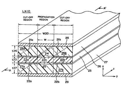
In Fig. 1, a dielectric substrate 23 has a
predetermined thickness t23 and a predetermined width
W20, with its length being sufficiently longer than its
width W20. On the top surface of the dielectric
substrate 23, electrodes 21a and 21b are provided
opposedly facing each other across a predetermined
spacing. With this arrangement, a slot 24 having width W
is formed between the electrodes 21a and 21b. The slot is
located in the central portion of the dielectric
substrate 23 along its width and in parallel to the
longitudinal direction of the substrate 23. Also, on the
bottom surface of the dielectric substrate 23, electrodes
22a and 22b are provided opposedly facing each other
across a predetermined spacing. With this arrangement, a
slot 25 having the same width W as the slot 24 is formed
between the electrodes 22a and 22b so that the slot 25 is
located in the central portion of the dielectric
substrate 23 along its width and in parallel to the
longitudinal direction of the substrate 23. The slots 24
and 25 are formed opposedly facing each other. The
dielectric substrate 23 interposed between the slots 24
and 25 serves as a propagation region 23c in which a
high-frequency signal having a desired propagation
frequency fb is transmitted, as will be described below
in a greater detail.
On the top surface of the dielectric substrate
23 having the electrodes 21a and 21b mounted thereon,
another dielectric substrate 26 with the same width W20
and length as the substrate 23 is provided. An electrode
- - 2.72888
- 10 -
28 is further mounted on the entire top surface of the
dielectric substrate 26. Also, on the bottom surface of
the dielectric substrate 23 having the electrodes 22a and
22b mounted thereon, a dielectric substrate 27 having the
same width W20 and length as the dielectric substrate 23
is located. An electrode 29 is disposed on the entire
bottom surface of the dielectric substrate 27.
The dielectric constant Er26 of the dielectric
substrate 26 is set to be equal to the dielectric
constant er27 of the dielectric substrate 27. On the
other hand, the dielectric constant Er23 of the
dielectric substrate 23 is set larger than the dielectric
constant er26 and er27, as will be explained below.
Fig. 2 shows a plane electromagnetic wave pw23
that is incident onto the top surface of the dielectric
substrate 23 in the slot 24 at an incidence angle 8 and
is reflected at an reflection angle 8 equal to the
incidence angle. The top surface of the dielectric
substrate 23 in the slot 24 forms a boundary between the
dielectric substrates 23 and 26. The plane
electromagnetic wave pw23, reflected on the top surface
of the dielectric substrate 23 in the slot 24, is
incident onto the bottom surface of the dielectric
substrate 23 in the slot 25 at an incident angle 8 and is
reflected at an reflection angle B equal to the incidence
angle. The bottom surface of the dielectric substrate 23
in the slot 25 constitutes a boundary between the
dielectric substrates 23 and 27. Thereafter, the
electromagnetic wave pw23 propagates as a transverse
electric (TE) mode within the propagation region 23c of
the dielectric substrate 23 while being repeatedly
reflected alternately on the top surface of the
2172888
- 11 -
dielectric substrate 23 in the slot 24 and on the bottom
surface of the substrate 23in the slot 25. An
electromagnetic wave propagating in the TE mode will
hereinafter be referred to as a "TE wave".
The angle 8 can be expressed by the following
equation 1 using the propagation constant kl of the plane
electromagnetic wave pw23 and the phase constant 8 of the
TE wave propagating in the longitudinal direction of the
dielectric substrate 23.
B = sin'1 (~/kl) .... Equation 1
If the incidence angle 8 is larger than the
critical angle 9dc expressed by the following equation 2,
the electromagnetic wave pw23 is totally reflected on the
top surface of the dielectric substrate 23 in the slot 24
and the bottom surface of the substrate 23 in the slot
25, thus propagating within the propagation region 23c of
the substrate 23 without being attenuated.
9dc = siril {~(ef26/er23) }
- siril {~(er27/Er23) } .... Equation 2
On the other hand, if the incidence angle 8 is
smaller than the critical angle Bdc, the electromagnetic
wave pw23 partially permeates into the dielectric
substrate 26 or the substrate 27, whereby the wave pw23
is attenuated.
The propagation constant k is determined by the
frequency of the plane electromagnetic wave pw23 and the
dielectric constant E~23 of the dielectric substrate 23.
The phase constant ~ is defined by the frequency of the
electromagnetic wave pw23, and the dielectric constant
er23 and the thickness t of the dielectric substrate 23.
It will now be assumed that x, y and z axes are
determined, as illustrated in Fig. 2, and that a TE wave
2172888
- 12 -
travels along the z axis while having the constant y
component of an electric field Ey. The propagation
constant kl of the planar wave propagating through the
dielectric substrate 23 can be expressed by the following
equation 3 utilizing the dielectric constant er23 of the
dielectric substrate 23.
kl = ka~/ ( sr23 ) . . . . Equation 3
Similarly, the propagation constant k2 of the planar wave
propagating through the dielectric substrate 26 can be
expressed by the following equation 4 utilizing the
dielectric constant et26 of the dielectric substrate 26:
k2 = ko,/ ( er26 ) . . . . Equation 4
wherein ko represents the propagation constant of the
planar wave in a vacuum. Since the phase constant B of
the planar wave propagating in the dielectric substrate
23 is equal to that in the dielectric substrate 26, the
following equation 5 can hold true:
~Z = k12-kxl2 = k22-kx2 .... Equation 5
wherein kxl and kx2 respectively indicate x components of
the propagation constants kl and k2 of the planar waves
propagating through the dielectric substrates 23 and 26.
The relation between the propagation constants kxl and kx2
can be expressed by the following equation 6:
(1/kxl)tan~ (kxl~(t23/2) }-(1/kx2)tan(kxZ~t26) - 0
.... Equation 6
Equations 5 and 6 are solved to obtain the propagation
constants kxl and kx2 and the phase constant ~B .
The lower the frequency of the plane
electromagnetic wave pw23 is, the smaller the incidence
angle 8 is. Hence, as long as the frequency of the
electromagnetic wave pw23 is not lower than the critical
frequency fda at which the incidence angle 8 is
2172888
- 13 -
equivalent to the critical angle 9dc, the wave will
propagate through the dielectric substrate 23 repeating
the total reflection on the surface of the dielectric
substrate 23 in the slot 24 and on the bottom surface of
the substrate 23 in the slot 25. The dielectric constant
er23 and the thickness t23 of the dielectric substrate 23
and the dielectric constant er26 and er27 of the
substrates 26 and 27, respectively, are set so that a
propagation frequency fb is not lower than the critical
frequency fda. In other words, the dielectric constant
E~23 and the thickness t23 of the dielectric substrate 23
and the dielectric constant e,26 and e,27 of the
substrates 26 and 27, respectively, are set so that a
planar wave having a propagation frequency fb is totally
reflected on the top surface of the dielectric substrate
23 in the slot 24 and on the bottom surface of the
substrate 23 close to the slot 25.
The electrodes 21a and 22a, formed opposedly
facing each other on the dielectric substrate 23,
constitute a planar-parallel waveguide having a cut-off
frequency sufficiently higher than the propagation
frequency fb with respect to the TE wave. This forms a
TE-wave cut-off region 23a in the dielectric substrate
23. Likewise, the electrodes 21b and 22b, disposed
opposedly facing each other, serve as a planar-parallel
waveguide having a cut-off frequency sufficiently higher
than the propagation frequency fb with respect to the TE
wave. This forms a TE-wave cut-off region 23b along the
width of the dielectric substrate 23 in a position
opposite to the cut-off region 23a.
Further, the electrode 21a and the portion of
the electrode 28 facing each other constitute a
- 21728~b
- 14 -
planar-parallel waveguide. The thickness t26 of the
substrate 26 is set so that the cut-off frequency with
respect to the TE wave passing through the plane-parallel
waveguide is sufficiently higher than the propagation
frequency fb. Accordingly, a TE-wave cut-off region 26a
is formed in the dielectric substrate 26. Similarly, the
electrode 21b and the portion of the electrode 28 facing
each other constitute a planar-parallel waveguide. A
TE-wave cut-off region 26b is thus formed in the
dielectric substrate 26 in a position opposite to the
cut-off region 26a. Moreover, in the dielectric
substrate 27, a planar-parallel waveguide is defined by
the electrode 22a and the portion of the electrode 29
opposedly facing each other. The thickness t27 of the
dielectric substrate 27 is set so that the TE-wave
cut-off frequency of the plane-parallel waveguide is
sufficiently higher than the propagation frequency fb.
This forms a TE-wave cut-off region 27a in the dielectric
substrate 27. Likewise, a TE-wave cut-off region 27b is
formed in the dielectric substrate 27, interposed between
the electrode 22b and the electrode 29 opposedly facing
each other, in a position opposite to the cut-off region
27a.
In the planar dielectric line LN10 of the first
embodiment, a propagation region 23c is defined in which
a high-frequency signal having a frequency not lower than
the critical frequency fda repeats total reflection
alternately on the top surface of the dielectric
substrate 23 in the slot 24 and on the bottom surface of
the substrate 23 in the slot 25. The cut-off regions
23a, 23b, 26a, 26b, 27a and 27b are, on the other hand,
formed to attenuate the high-frequency signal. With this
configuration of the line LN10, a TE wave having a
21'~28~8
- 15 -
frequency not lower than the critical frequency fda
propagates through the dielectric substrate 23 of the
dielectric line LN10 in the longitudinal direction while
concentrating its electromagnetic-field energy inside and
in the vicinity of the propagation region 23c.
Also, since the planar dielectric line LN10
comprises the dielectric substrates 23, 26 and 27, it is
possible for shorter wavelengths of electromagnetic waves
to propagate in the dielectric substrates 23, 26 and 27
than in free space. This further makes it possible to
decrease the width and the thickness of the dielectric
line LN10 which can thus be made smaller and lighter than
a square waveguide.
The planar dielectric line LN10 further
comprises the electrodes 21a and 21b mounted on the top
surface of the dielectric substrate 23 and electrodes 22a
and 22b on the bottom surface thereof. The widths W of
the slots 24 and 25 are narrow so that other types of
electronic parts, such as ICs or the like, can be
directly connected to the electrodes 21a and 21b or the
electrodes 22a and 22b without requiring additional
connecting parts, as implemented in the slotted line of
the prior art, thereby enabling easy connection between
the planar dielectric line LN10 and the other electronic
parts, such as ICs.
Fig. 12 is a cross sectional view of a planar
dielectric line LN20 according to a second embodiment of
the present invention. The dielectric line LN20 differs
from the dielectric line LN10 in that upper and lower
conductive plates 41a and 41b are employed in place of
the dielectric substrate 26 and 27 having electrodes 28
and 29.
21'2888
- 16 -
On the top surface of the substrate 23, the
electrodes 21a and 21b are provided opposedly facing each
other forming a slot 24. Also, on the bottom surface of
the dielectric substrate 23, electrodes 22a and 22b are
provided opposedly facing each other forming a slot 25.
The upper and lower conductive plates 41a and 41b are
provided in parallel to each other across a spacing h41.
The dielectric substrate 23 provided with the slots 24
and 25 is disposed in parallel to the upper and lower
conductive plates 41a and 41b. The distance between the
upper conductive plate 41a and the top surface of the
substrate 23 is set to be equal to the distance between
the lower conductive plate 41b and the bottom surface of
the substrate 23.
In the dielectric line LN20, the dielectric
constant E,23 of the dielectric substrate 23 is
determined as follows . The ref lection of an
electromagnetic wave on the top surface of the substrate
23 in the slot 24 and on the bottom surface of the
substrate 23 in the slot 25 occurs, unlike the first
embodiment, at a boundary between the dielectric
substrate 23 and free space. The critical angle Bc can,
therefore, be expressed by the following equation 7
utilizing the dielectric constant Er = 1 of free space:
8c = siril~,/(1/E~23) } . . . . Equation 7
Accordingly, in the planar dielectric line LN20
of this embodiment, the electromagnetic wave pw23 having
a frequency not lower than the critical frequency fa at
which the angle of reflection 8 becomes equal to the
critical angle 6c propagates while repeating the total
reflection on the top surface of the dielectric substrate
23 in the slot 24 and on the bottom surface of the
- 2172g~~
- 17 -
substrate 23 in the slot 25. The dielectric constant
Er23 and the thickness t23 of the substrate 23 are set so
that the propagation frequency fb is not lower than the
critical frequency fa.
A plane-parallel waveguide is defined by the
electrode 21a and the upper conductive plate 41a
opposedly facing each other. The spacing h41 between the
upper and lower conductive plates 41a and 41b is set so
that the TE-wave cut-off frequency of the above-mentioned
plane-parallel waveguide is sufficiently higher than the
propagation frequency fb. A TE-wave cut-off region 42a
located between the electrode 21a and the upper
conductive plate 41a facing each other is thus formed in
part of the free space interposed between the dielectric
substrate 23 and the upper conductive plate 41a.
Likewise, a plane-parallel waveguide is specified by the
electrode 21b and the upper conductive plate 41a facing
each other. A TE-wave cut-off region 42b between the
electrode 21b and the upper conductive plate 41a is thus
formed in free space sandwiched between the substrate 23
and the upper conductive plate 41a, in a position
opposite to the cut-off region 42a.
As described above, the distance between the
upper conductive plate 41a and the top surface of the
dielectric substrate 23 is determined equal to the
distance between the lower conductive plate 41b and the
bottom surface of the substrate 23. Accordingly, a
plane-parallel waveguide having a TE-wave cut-off
frequency adequately higher than the propagation
frequency fb is defined by the electrode 22a and the
lower conductive plate 41b opposedly facing each other.
A TE-wave cut-off region 43a clamped between the
272888
- 18 -
electrode 22a and the lower conductive plate 41b is thus
formed in part of the free space interposed between the
substrate 23 and the lower conductive plate 41b.
Similarly, a TE-wave cut-off region 43b sandwiched
between the electrode 22b and the lower conductive plate
41b facing each other is thus defined in the free space
in a position opposite to the cut-off region 43a.
In the planar dielectric line LN20, a
propagation region 23c is constructed in which a
high-frequency signal having a frequency not lower than
the critical frequency fa is transmitted in the
dielectric substrate 23 while repeating the total
reflection alternately on the top surface of the
substrate 23 in the slot 24 and on the bottom surface of
the substrate 23 in the slot 25. On the other hand, in
the cut-off regions 23a, 23b, 42a, 42b, 43a and 43b the
high-frequency signal is attenuated. With this
construction, a signal having a frequency not lower than
the critical frequency fa propagates in the planar
dielectric line LN20 while concentrating its
electromagnetic energy inside and in the vicinity of the
propagation region 23c.
In the second embodiment, the upper and lower
conductive plates 41a and 41b are employed in place of
the dielectric substrates 26 and 27 used in the first
embodiment. This enhances easier construction of the
dielectric line LN20 than the dielectric line LN10 of the
first embodiment, which leads to a decrease in costs.
A detailed explanation will now be given of the
principle of the operation of the dielectric line LN20
according to the second embodiment. Prior to an
explanation of this line LN20, a dielectric-loaded
2~72~~8
- 19 -
waveguide line LN30 operated similar to the line LN20
will first be described.
The dielectric-loaded waveguide line LN30, as
illustrated in Fig. 3, comprises a square waveguide 36
having an internal width W36 and an internal height h36,
and a dielectric substrate 33 having a thickness t33 and
a width equal to the width W36 of the waveguide 36. The
dielectric substrate 33 is disposed at a central location
with respect to the height of the square waveguide 36 so
that it can be located in parallel to the upper and lower
conductive plates of the waveguide 36. The dielectric
constant er33 of the dielectric substrate 33 shall be set
to equal the dielectric constant e~23 of the dielectric
substrate 23 of the second embodiment.
A high-frequency signal having a frequency not
lower than the critical frequency fa is input into the
waveguide line LN30 shown in Fig. 3 and is propagated in
the substrate 33 in the longitudinal direction while
concentrating its electromagnetic energy inside and in
the proximity of the substrate 33. The
electromagnetic-field distribution obtained during the
propagation of the signal in the waveguide 36 is
indicated in Figs. 4A and 4B. Fig. 4A illustrates an
electric field E30 and a magnetic field H30 in a cross
sectional view along line C-C' of Fig. 3. Fig. 4B
illustrates the electric field E30 and the magnetic field
H30 in a longitudinal sectional view along line B-B' of
Fig. 3. Figs. 4A and 4B clearly show that the electric
field E30 and the magnetic field H30 are distributed
inside and in the vicinity of the dielectric substrate
33. The electric field E30 has only a component in the
widthwise direction of the substrate 33, while the
- ~1 X2888
- 20 -
magnetic field H30 has both a component in the
longitudinal direction of the substrate 33, i.e., the
longitudinal direction of the waveguide 36, and a
component perpendicular to the top surface or the bottom
surface of the substrate 33.
In contrast, Figs. ilA and 11B illustrate an
electromagnetic-field distribution obtained when a
high-frequency signal having a frequency lower than the
critical frequency fa is input into the dielectric-loaded
waveguide line LN30. Fig. 11A illustrates the electric
field E30 and the magnetic field H30 in a cross sectional
view along line C-C' of Fig. 3. Fig. liB illustrates the
electric field E30 and the magnetic field H30 in a
longitudinal sectional view along line B-B' of Fig. 3.
As is seen from Fig. 11A and 11B, the magnetic field H30
is distributed farther away from the substrate 33 than
the magnetic field of the frequency not lower than the
critical frequency fa shown in Figs. 4A and 4B, and
further, as seen in Fig. 11A, the electric field E30 has
a component outside the substrate 33.
Fig. 5 is a diagram indicating the relation
between the frequency and the phase constant X30 of the
dielectric-loaded waveguide line LN30 when the dielectric
constant Er33 of the substrate 33 was varied to have the
values 2, 5, 9.3 and 24. The values indicated in Fig. 5
were calculated according to equations 5 and 6. The
parameters of the structure of the waveguide line LN30
were set as follows:
(1) The thickness t33 of the substrate 33 =
0.33 mm; and
(2) The height h36 of the waveguide 36 = 2.25
mm
- 2~ 72888
- 21 -
Fig. 5 reveals that a higher frequency causes a larger
phase constant X30 and that a greater dielectric constant
er33 gives rise to a larger phase constant X30 under the
condition of the same frequency.
Fig. 6 is a diagram representing the relation
between the frequency and the phase constant X830 of the
waveguide line LN30 obtained when the thickness t of the
substrate 33 was varied to have the values 0.1 mm, 0.33
mm, 0.5 mm and 1 mm. The values shown in Fig. 6 were
calculated according to equations 5 and 6. The
parameters of the structure of the waveguide line LN30
were set as follows:
(1) The dielectric constant er33 of the
substrate = 9.3; and
(2) The internal height h36 of the waveguide
36 = 2.25 mm
Fig. 6 demonstrates that a greater thickness
t33 of the substrate 33 causes a greater phase constant
X830 under the condition of the same frequency.
Next, the critical frequency fa at which the
incidence angle 8 is equal to the critical angle 8c will
be calculated with the use of the dielectric-loaded
waveguide line LN30.
Fig. 7 is a diagram indicating the relation
between the critical frequency fa at which the incidence
angle 8 is equal to the critical angle 8c and the
dielectric constant Er33 of the substrate 33. The
parameters of the structure of the waveguide line LN30
were set as follows:
(1) The thickness t33 of the substrate
33 = 0.33 mm;
__ 2172888
' - 22 -
(2) The internal width W36 of the waveguide
36= 2.0 mm; and
(3) The internal height h36 of the waveguide
36 = 2.25 mm.
As is seen from Fig. 7, a greater dielectric constant
er33 of the substrate 33 brings about a lower critical
frequency fa. Namely, with a dielectric substrate 33
having a higher dielectric constant Er33, the minimum
propagation frequency fb of a totally-ref lecting
high-frequency signal can be reduced to a lower level.
Fig. 8 is a diagram representing the relation
between the critical frequency fa at which the incidence
angle 8 is equal to the critical angle 8c and the
thickness t33 of the substrate 33. The parameters of the
structure of the waveguide line LN30 were set as follows:
(1) The dielectric constant er33 of the
substrate 33 = 9.3;
(2) The internal width W36 of the waveguide
36 = 2.0 mm; and
(3) The internal height h36 of the waveguide
36 = 2.25 mm.
Fig. 8 reveals that a greater thickness t33 of
the substrate 33 causes a lower critical frequency fa at
which the incidence angle 8 is equal to the critical
angle Bc. That is, by increasing the thickness t33 of
the substrate 33, the minimum propagation frequency fb of
a totally reflecting high-frequency signal can be reduced
to a lower level.
Based on the operation principle of the
waveguide line LN30 explained above, the operation of the
planar dielectric line LN20 (Fig. 12) of the second
embodiment will now be described. The critical frequency
- ~17~8~8
' - 23 -
fa of the dielectric line LN20 was calculated from the
critical frequency fa of the dielectric line LN30 when
the parameters of the line LN20 were set as follows:
(1) The thickness t23 of the substrate
23 = 0.33 mm;
(2) The width W20 of the substrate 23 = 8 mm;
and
(3) The widths W of the slots 24 and 25 =
2 mm.
The dielectric constant er23 and the thickness t23 of the
substrate 23 are respectively set equal to the dielectric
constant er33 and the thickness t33 of the substrate 33.
Also, the widths W of the slots 24 and 25 of the
substrate 23 are set equal to the internal width W of the
waveguide 36. The spacing h41 between the upper and
lower conductive plates 41a and 41b is set equivalent to
the internal height h36 of the waveguide 36.
Fig. 9 is a diagram designating the relation
between the frequency and the phase constant X820 of the
dielectric line LN20 when the dielectric constant e~23 of
the substrate 23 was set at the values 2, 5, 9.3 and 24.
The values shown in Fig. 9 were calculated according to
the finite-element method. Fig. 9 demonstrates that a
higher frequency gives rise to a greater phase constant
X20 and a greater dielectric constant E,23 brings about a
greater phase constant X20 under the condition of the
same frequency.
Fig. 10 is a diagram indicating the relation
between the frequency and the phase constant X20 of the
dielectric line LN20 when the widths W of the slots 24
and 25 of the substrate 23 were set at the values 0.5 mm,
1 mm, 2 mm and 3 mm. The values shown in Fig. 10 were
-- 21'2888
' - 24 -
calculated according to the finite-element method. The
parameters of the structure of the dielectric line LN20
were set as follows:
(1) The dielectric constant ef23 of the
substrate 23 = 9.3;
(2) The width W20 of the substrate 23 = 8 mm;
and
(3) The spacing h41 between the upper and
lower conductive plates 41a and 41b = 2.25
mm.
Fig. 10 shows that a greater width W of the
slots 24 and 25 causes a lower phase constant X20 under
the condition of the same frequency.
A further explanation will further be given of
the electromagnetic-field distribution of the dielectric
line LN20 (Fig. 12) according to the second embodiment.
Fig. 13 illustrates the electromagnetic-field
distribution in a perspective view of the dielectric
substrate 23 as a comparative example when a
high-frequency signal having a frequency lower than the
critical frequency fa is input into the dielectric line
LN20. In Fig. 13, the upper and lower conductive plates
41a and 41b are omitted and only the dielectric substrate
23 is shown. Also in the perspective view of Fig. 13,
the top portions of the electrodes 21a and 21b are
hatched for easy differentiation. As is clearly seen
from Fig. 13, both the electric field E20 and the
magnetic field H20 are distributed farther away from the
vicinity of the substrate 23 than the
electromagnetic-field distribution achieved at a
frequency not lower than the critical frequency fa, as
shown in Fig. 14.
2I728~~
' - 25 -
Fig. 14 illustrates the electromagnetic
distribution when a high-frequency signal having a
frequency not lower than the critical frequency fa is
input into the dielectric line LN20. In Fig. 14, as well
as Fig. 13, the upper and lower conductive plates 41a and
41b are omitted and only the substrate 23 is shown.
Also, in the perspective view of Fig. 14, the top
surfaces of the electrodes 21a and 21b are hatched for
easy differentiation. Fig: 14 reveals that both the
electric field E20 and the magnetic field H20 are
concentrated only inside and in proximity of the
propagation region 23c of the substrate 23d. More
specifically, it is seen that a high-frequency signal
having a frequency not lower than the critical frequency
fa is totally reflected by top surface of the substrate
23 adjacent to the slot 24 and by the bottom surface of
the substrate 23 in the vicinity of the slot 25.
Although only the operation of the dielectric
line L20 has been discussed above, the dielectric line
LN10 of the first embodiment is operated in a manner
similar to the line LN20. As has been described above in
detail, both the planar dielectric line LN10 of the first
embodiment and the line LN20 of the second embodiment are
operated in a manner similar to the dielectric-loaded
waveguide line LN30 and used for transmitting a
high-frequency signal having a frequency not lower than
the critical frequency fa.
The present inventors observed the
electric-field distribution by use of the model shown in
Fig. 15 in order to examine the operation performed when
two or more planar dielectric lines are disposed in
proximity to each other. The.construction of the model
and results will be explained. In the model shown in
- 2I72~~8
- 26 -
Fig. 15, the electrodes 121a, 121b, 121c and 121d and the
slots 124x, 124b and 124c are alternately formed on the
top surface of the substrate along its width. More
specifically, the slot 124a is disposed between the
electrodes 121a and 121b; the slot 124b is located
between the electrodes 121b and 121c; and the slot 124c
is interposed between the electrodes 121c and 121d. The
slots 124a, 124b and 124c are formed in parallel to the
longitudinal direction of the substrate 23 and also have
the same widths. The electrodes 121b and 121c also have
the same widths.
Mounted on the bottom surface of the substrate
123 are electrodes 122a and 122b opposedly facing the
electrodes 121a and 121b, respectively, across the
substrate 123. Also, electrodes 122c and 122d are
disposed opposedly facing the electrodes 121c and 121d,
respectively, across the substrate 123. With this
arrangement, slots 125a, 125b and 125c are located
opposedly facing the slots 124a, 124b and 124c,
respectively. The substrate 123 is disposed between the
upper and lower conductive plates 141a and 141b in
parallel to each other so that it can be placed in
parallel thereto. The distance between the top surface
of the substrate 123 and the upper conductive plate 141a
can be equal to the distance between the bottom surface
of the substrate 123 and the lower conductive plate 141b.
Moreover, the upper and lower conductive plates 141a and
141b are spaced apart from each other in a manner similar
to the second embodiment. The three planar dielectric
lines in parallel to each other are thus constructed.
Fig. 15 illustrates an electric field E120
obtained when high-frequency signals having a frequency
not lower than the critical frequency fa are transmitted
- 27 -
in the three plane dielectric lines. Fig. 15 shows that
the signals are transmitted in the longitudinal direction
of the substrate 123 without interfering with each other.
Fig. 16 indicates an electric field E12 resulting when
high-frequency signals having a frequency lower than the
critical frequency fa are transmitted in the three lines.
Fig. 16 reveals that high-frequency signals suffer from
electromagnetic-field coupling, i.e., electromagnetic-
ffield interference.
As has been discussed above in detail, in the
respective planar dielectric lines LN10 and LN20 of the
first and second embodiments, a high-frequency signal
having a frequency not lower than the critical frequency
fa is totally reflected on the top surface of the
substrate 23 adjacent to the slot 24 and on the bottom
surface of the substrate 23 in the vicinity of the slot
25, whereby the signal can be propagated while
concentrating its electromagnetic-field energy inside and
in the proximity of the propagation region 23c of the
substrate 23. To further develop these embodiments, it
is possible to dispose a plurality of planar dielectric
lines in parallel to each other along the width of the
substrate 123, thus enabling the formation of
highly-integrated circuits.
Fig. 17 is a perspective view of an integrated
circuit produced by the application of the planar
dielectric line according to the present invention. This
integrated circuit is configured to have a
generally-square dielectric substrate 323 provided with a
plurality of dielectric lines. An electrode 321 with a
predetermined shape is mounted on the top surface of the
substrate 323, while an electrode 322 with a
predetermined shape is formed on the bottom surface of
2~~2888
- 28 -
the substrate 323, both the electrodes 321 and 322
opposedly facing each other. Accordingly, planar
dielectric lines LN301, LN302, LN303 and LN304, a high
pass filter 310, and biasing lines 307 and 308 are formed
on the dielectric substrate 323. On the top surface of
the substrate 323, a circuit part module 305 is connected
between the dielectric lines LN302 and LN303, while a
circuit part module 306 is connected between the
dielectric line LN301 and the biasing line 307. The bent
portions of the lines LN301 and LN303 are comprised of
line portions 301a and 303a, respectively, formed by the
narrowed slots. This makes it possible to bend the
dielectric lines LN301 and LN303 without requiring a
change from the propagation mode currently employed in
the lines LN301 and LN303 to another mode.
The high pass filter 310 will now be described.
Fig. 18 is a sectional view along line E-E' of Fig. 17.
As shown in Figs. 17 and 18, two circular openings 4c and
4d having the same diameter are formed on the top surface
of the substrate 323. On the other hand, two circular
openings 5c and 5d of the same size as the openings 4c
and 4d are formed on the bottom surface of the substrate
323. The openings 4c and 4d are disposed between the
dielectric lines LN303 and LN304 so that they can be
located in parallel to each other across a predetermined
spacing. Also, the openings 4d and 5d are coaxially
formed to opposedly face each other. With this
construction, two cylindrical resonator-forming regions
66 and 69 of the same shape are located between the
dielectric lines LN303 and LN304. The resonator region
66, which is part of the substrate 323, is defined as a
cylindrical region having the surface 67 of the opening
4c in the substrate 323 and the surface 68 of the opening
21'~28~~
- 29 -
5c in the substrate 323. The resonator region 69, on the
other hand, which is part of the substrate 323, is
defined as a cylindrical region having the surface 70 of
the opening 4d in the substrate 323 and the surface 71 of
the opening 5d in the substrate 323.
The dielectric constant and the thickness of
the substrate 323 and the diameters of the openings 4c,
4d, 5c and 5d are so determined as to generate a standing
wave when the resonator regions 66 and 69 are excited by
a high-frequency signal having the same frequency as a
resonance frequency. Further, in the regions other than
the resonator regions 66 and 69 and the propagation
regions, i.e., dielectric lines LN301, LN302, LN303 and
LN304, a planar-parallel waveguide is formed by
electrodes 321 and 322. The dielectric constant and the
thickness of the substrate 323 are also determined so
that the cut-off frequency of the plane-parallel
waveguide will be higher than a desired resonance
frequency. With this arrangement, the resonator region
66 and adjacent free space, and the resonator region 69
and free space in the vicinity thereof, respectively
constitute TEoio mode-dielectric resonators. The regions
66 and 69 are separated from each other across a
predetermined spacing so that the dielectric line LN303
and the TEolo mode-dielectric resonator formed by the
region 66 can be inductively coupled. The distance
between the dielectric line LN304 and the region 69 is
determined so that the dielectric line LN304 and the TEolo
mode-dielectric resonator formed by the region 69 can be
inductively coupled.
In this manner, the high pass filter 310 is
constructed by the cascade connection of the two TEolo
2I72~88
- 30 -
mode dielectric resonators between the dielectric lines
LN303 and LN304. This causes a high-frequency signal
having a predetermined frequency passing through the
dielectric line LN303 being transmitted to the line LN304
through the two TEolo mode-dielectric resonators.
Examples of modifications of the present
invention will now be explained.
The planar dielectric line LN10 of the first
embodiment is comprised of the dielectric substrates 26
and 27, while the dielectric line LN20 of the second
embodiment is formed with the use of the upper and lower
conductive plates 41a and 41b. However, this is not
exclusive, and the dielectric line may use only the
dielectric substrate 23 provided with the slots 24 and
25. This modification also makes it possible to operate
in a manner similar to the first and second embodiments
and offers similar advantages, with a simpler
construction.
Although the upper and lower conductive plates
41a and 41b are used for the dielectric line LN20 of the
second embodiment, as described above, the present
invention is not limited thereto. Instead, a square
waveguide defined by the upper and lower conductive
plates 41a and 41b and lateral-surface conductors may be
employed to form the line. With this modification, it is
also possible to operate in a manner similar to the first
and second embodiments and offer similar advantages.
In the dielectric line LN20 of the second
embodiment, the distance between the upper conductive
plate 41a and the top surface of the substrate 23 is
determined to equal the distance between the lower
conductive plate 41b and the bottom surface of the
_ 2172888
- 31 -
substrate 23. However, this is not exclusive, and the
former distance may differ from the latter distance. The
line obtained by the above modification is still operable
in a manner similar to the first and second embodiments
and can present the similar advantages.
Further, although the dielectric constant Er26
of the dielectric substrate 26 is determined to be equal
to the dielectric constant Er27 of the substrate 27, they
may differ from each other.
As will be clearly understood from the
foregoing description, the present invention offers the
following advantages.
In the planar dielectric line according to a
first aspect of the present invention, a first slot
having a predetermined width is formed on the first
surface of the dielectric substrate, and a second slot is
mounted on the second surface of the substrate, both the
slots facing each other. This makes it possible to
provide a small and inexpensive planar dielectric line
that can enhance easier connection with electronic parts,
such as ICs, and inhibit conductor losses to a lower
level than microstrip lines, coplanar lines and slotted
lines.
The planar dielectric line according to a
second aspect of the present invention is constructed by
adding first and second conductive plates to the planar
dielectric line implemented by the first aspect of the
present invention. It is thus possible to prevent
leakage to the exterior of high-frequency signals
propagating in the above-described dielectric line and
also to preclude the entry of high-frequency signals from
the exterior of the dielectric line.
2172888
- - 32 -
In the planar dielectric line according to a
third aspect of the present invention, the following
features are added to the dielectric line implemented by
the second aspect of the present invention. Namely, a
dielectric is charged between the first surface of the
dielectric substrate and the first conductive plate, and
another dielectric is interposed between the second
surface of the substrate and the second conductive plate,
each dielectric having a smaller degree of permittivity
than the dielectric substrate. The planar dielectric
line can thus be made thinner.
An integrated circuit according to a fourth
aspect of the present invention comprises a transmission
line and a high-frequency device connected to the
transmission line. The transmission line includes at
least one of the planar dielectric lines implemented by
the first to third aspects of the present invention.
Accordingly, a highly-integrated circuit can be
constructed.