Note: Descriptions are shown in the official language in which they were submitted.
WO 95/10808 PCT/US94/03241
1
VIRTUAL ADDRESS TRANSLATION HARDWARE ASSIST
CIRCUIT AND METHOD
FIELD OF THE INVENTION:
This invention relates generally to digital data processors and, in
particular, to
circuits and methods for use in translating a virtual address to a physical
memory
address.
BACKGROUND OF THE INVENTION:
Data processing systems that employ virtual addressing techniques are well
represented in the prior art. By example, the following U.S. Patents all
disclose
subject matter that is related to the translation of virtual addresses into
real or
physical memory addresses.
In U.S. Patent 4,128,875, 12/5/78, "Optional Virtual Memory System", K.
Thurber
et al. describe a memory addressing mechanism that works with three address
structures: real, based, and virtual. Table II of this patent describes
virtual
address translation steps of the prior art (referenced to Figure 8). For a
four
segment computer address containing process, segment, page and offset
identifiers,
the translation steps are said be as follows.
1. Reference memory into process table using process number for offset and a
predetermined reference.
2. Obtain segment pointer frono poocec~ table reference .
3. Reference memory into segment, taple using segment pointer as reference
and segment number as offset.
4. Obtain page pointer from segment table reference.
5. Reference memory into page table using page pointer as reference and page
number as offset.
6. Obtain frame number from page table reference.
WO 95/10808 PCT/US94/03241
7. Concatenate frame number with deflection to obtain real memory address.
8. Reference memory using real memory address.
A total of four memory references are thus required (steps 1, 3, 5, and 8).
In U.S. Patent 4,638,426, 1/20/87, "Virtual Memory Address Translation
Mechanism with Controlled Data Persistence", A. Chaug et al. describe a two
step
address translation function and the use of a Translation Look-Aside Buffer
(TLB).
In U.S. Patent 4,680,700, 7/14/87, "Virtual Memory Address Translation
Mechanism with Combined Hash Address Table and Inverted Page Table", P.
Hester et al. describe a translation mechanism that includes a combined table
in
memory which stores as a first list the respective victual address of each
memory
address, referred to as an Inverted Page Table, and a second list that
connects
each of a plurality of hashed addresses with a predetermined initial virtual
address of a linked group of virtual addresses.
In U.S. Patent 4,714,993, 12/22/87, "Apparatus and Method for Effecting
Dynamic
Address Translation in a Microprocessor Implemented Data Processing System",
D. Livingston et al. describe the use of a RAM-based storage unit that
functions
as a page address table. Circuitry, including microcode, is employed to
initialize
and update the contents of the storage unit as required. The storage unit is
coupled to an address bus of a microprocessor from whence it receives the page
portion of a virtual address to be translated.
In U.S. Patent 4.096.568, 6/20/ 7 8. "Vi.rtual. Address Translatoz-". D.
Bennett et al.
describe the use of a content addressable memory ( CAM) and a word addressed
memory in a virtual address translator. A task name and subsegment number are
used as a key to search the content addressable memory. A subsegment
descriptor
read out of the content addressable memory includes an absolute base address
which is added to a deflection field to obtain an absolute memory address.
CA 02173225 2002-12-10
77215-11
3
Finally, in commonly assigned U.S. Patent
4,410,941, 10/18/83, "Computer Having an Indexed Local RAM
to Store Previously Translated Virtual Addresses", A. Barrow
et al describe the use of Translation RAM (T/RAM) having a
capacity of one entry for each page of supported virtual
memory. The use of a monitor bit is also described for each
segment of virtual memory. At column 3, lines 3-12 a
translation process is described. The translation process
may be carried out by a processor executing microcode or by
dedicated hardware within the processor. The steps of the
translation process are said to include: (a) applying the
segment number to locate a page table; (b) applying the
virtual page number to address an entry within the page
table; (c) obtaining the page table entry; (d) checking the
state of a fault bit; and (if the page is in main memory)
(e) combining the page frame number with an offset from the
virtual address to form a physical address.
Pages 586-589 of the document 1987 IEEE
International Conference on Computer Design: VLSI in
Computers & Processors, 5 October 1987, Holden et al.
'Integrated memory management for the MC68030', disclose a
virtual address translation method/system whereby a
microcoded memory management unit produces a translation
buffer entry (physical address) from a logical (virtual)
address containing a plurality of descriptor fields.
Descriptor table entries are accessed by adding an
appropriate field to a previously accessed descriptor field.
One problem that is presented when a data
processor employs a microcoded-approach to virtual address
translation is related to the significant number of micro-
instructions that must be executed to perform the
CA 02173225 2002-12-10
77215-11
3a
translation. More particularly, in that each micro-
instruction consumes some portion of the data processor's
instruction execution bandwidth, it is desirable to make the
virtual address translation process as rapid as possible,
such as by reducing the total number of micro-instructions
that are required to perform the translation. Reducing the
number of micro-instructions would not only yield a
corresponding improvement in processor performance, but
would also reduce the storage requirements of a micro-code
control store. Related to the desired improvement in
translation time is an ability to rapidly detect the
presence of anomalous conditions, such as a faulted zone,
segment, or page, that may arise during the translation
process, and to provide an efficient mechanism to report and
act on the detection of the anomalous translation condition.
OBJECTS OF THIS INVENTION
It is thus a first object of this invention to
provide a hardware-assisted virtual address translation
technique that overcomes the foregoing and other problems of
the prior art.
WO 95/10808 PCT/US94/03241
4
It is another object of this invention to provide a hardware-assisted virtual
address
translation technique that provides for- a significant reduction in a required
number of micro-instructions to achieve the virtual address translation.
It is a further object of this invention to provide a hardware-assisted
virtual
address translation technique that provides for the rapid detection and
reporting
of translation anomalies in parallel and simultaneous with the execution of
certain
steps of the translation process.
SUMMARY OF THE INVENTION
The foregoing and other problems are overcome and the objects of the invention
are realized by circuitry and a method of providing hardware-assisted virtual
memory address translation. The hardware-assist circuitry is designed to
assist
the data processor in the determination of a physical memory address for a
given
virtual address. The design is such that the memory access of an address
pointer
and the addition of that base pointer to the appropriate table offset are
performed
simultaneously. The result of that addition is then loaded into a physical
memory
address register for the access of the next base pointer in a following micro-
cycle.
In parallel the detection of certain translation anomalies are detected and
reported
to a control program.
Previously, a virtual address translation sequence required as many as 22
micro-
instructions to accomplish. By employing the teaching of this invention the
total
number of micro-instructions has been reduced to nine. The use of this
invention
has thus also resulted in the saving of a significant number of valuable micro-
code
control store locations.
More particularly, this invention provides a method, and circuitry that
operates
in accordance with the method, for generating an entry for a translation
buffer in
a data processor that employs virtual memory addressing. The method includes
a first step of, in response to the execution of at least one micro-
instruction,
storing a Faulted Virtual Address in a first register. A Zone Table Address
(ZTA)
WO 95/10808 PCT/US94/03241
2I X322
is previously stored in a second register. In response to the execution of a
further
micro-instruction, a next step forms a first address in memory of a Zone Table
Entry (ZTE) by selectively combining the content of the first register with
the
content of the second register, while simultaneously testing the ZTA for
physical
address mapping. The first address is placed in a physical address register of
a
central processor. In response to an execution of a next micro-instruction, a
next
step forms a second address in memory of a Segment Table Entry (STE) by
accessing the ZTE with the first address, selectively combining the content of
the
first register with a content of the ZTE, while simultaneously testing the ZTE
for
a Zone fault. The second address is placed in the physical address register of
the
central processor. In response to an execution of a next micro-instruction, a
next
step forms a third address in memory of a Page Table Entry (PTE) by accessing
the STE with the second address, selectively combining the content of the
first
register with a content of the STE, while simultaneously testing the STE for a
Zone fault. The third address is placed in the physical address register of
the
central processor. In response to an execution of a next micro-instruction, a
next
step accesses the PTE with the third address, selectively combines the content
of
the STE with the content of the PTE, and outputs the combination as the
translation buffer entry, while simultaneously testing the PTE for a Page
fault.
The data processor has at least one central processor unit (CPU) that includes
a
translation buffer. The steps of selectively combining are accomplished by
circuitry
that is external to the CPU, and the steps of accessing are accomplished by
the
CPU.
The step of selectively combining the content of the STE witb. the content of
the
PTE includes the steps of: storing at least a portion of the content of the
STE; and
logically combining the stored portion with a portion of the content of the
PTE.
The step of outputting the combination includes a step of outputting a
physical
page number portion of the PTE with the logical combination.
CA 02173225 2003-12-19
77215-11
,.
6
The step of forming an address in memory of the
ZTE by selectively combining the content of the first
register with the content of the second register includes a
step of adding a physical address of the Zone Table in the
second register with a Zone field of the faulted virtual
address stored within the first register.
The step of forming an address in memory of the
STE by selectively combining the content of the first
register with the content of the ZTE includes a step of
concatenating a physical address of the Segment Table read
from the ZTE with a Segment field of the faulted virtual
address stored within the first register.
The step of forming an address in memory of the
PTE by selectively combining the content of the first
register with the content of the STE includes a step of
concatenating a physical address of the Page Table read from
the STE with a Page field of the faulted virtual address
stored within the first register.
If any of the steps of simultaneously testing
indicate a true condition, the method includes a step of
terminating the generation of the entry for the translation
buffer.
According to another aspect the invention provides
circuitry for assisting in the generation of an entry for a
translation buffer in a micro-coded data processor that
employs virtual memory addressing, comprising: first
register means for storing a Faulted Virtual Address and
second register means for storing a Zone Table Address
(ZTA), said first and second register means each being
loadable in response to the execution of preliminary
micro-instructions; means, responsive to the execution of a
first micro-instruction, for forming a first memory address
CA 02173225 2005-05-06
7721.5-11
6a
of a zone Table Entry (ZTE) in a zone table by selectively
combining a content of the first register with a content of
the second register; means, responsive to an execution of a
next, second micro-instruction, for accessing the ZTE with
the first memory address and for forming a second memory
address of a segment Table Entry (STE) in a segment table by
selectively combining the content of the first register with
a content of the ZTE; means, responsive to an execution of a
next, third micro-instruction, for accessing the STE with
the second memory address and for forming a third memory
address of a Page Table Entry (PTE) in a page table by
selectively combing the content of the first register with a
content of the STE; means, responsive to an execution of a
next, fourth micro-instruction, for accessing the PTE with
the third memory address and for selectively combining the
content of the STE with the content of the PTE and
outputting the combination as the translation buffer entry;
and means, responsive to the execution of the first micro-
instruction, for testing the ZTA for physical address
mapping, said testing means being further responsive to the
execution of the second micro-instruction for testing the
ZTE :for a Zone fault; to the execution of the third micro-
instruction for testing the STE for a Segment fault; and to
the execution of the fourth micro-instruction for testing
the PTE for a Page fault.
BRIEF DESCRIPTION OF THE DRAWINGS
The above set forth and other features of the
invention are made more apparent in the ensuing Detailed
Description of the Invention when read in conjunction with
the attached Drawings, wherein:
Fig. 1 illustrates the arrangement of Figs. 2A-2D;
CA 02173225 2004-07-06
77215-11
6b
Figs. 2A-2D are each a portion of a block diagram
of a data processor that is constructed and operated in
accordance with this invention;
Fig. 3 is a block diagram that illustrates in a
conceptual manner the translation of a virtual address to a
physical memory address;
WO 95/10808 2 PCT/US94/03241
7
Fig. 4A illustrates the format of a zone table address register;
Fig. 4B illustrates the format of a zone table entry;
Fig. 4C illustrates the format of a segment table entry;
Fig. 4D illustrates the format of a page table entry;
Fig. 4E illustrates the format of a translation buffer (TBUF) load format; and
Fig. 5 is a schematic diagram of circuitry that provides a hardware assisted
virtual
address translation function.
DETAILED DESCRIPTION OF THE INVENTION
Reference is made to Figs. 2A-2D for the ensuing description of a data
processor
that is constructed and operated in accordance with this invention. A Central
Processor (CP) 12 is coupled to an 8K by 88-bit Control Store 14 by a 14-bit
control
store address bus 14a and an 88-bit control store data bus 14b. The Control
Store
14 stores microinstructions which are read into the CP 12 in order to execute
macroinstructions that are read from an 8K by 72-bit CACHE memory 16, via a
CACHE Data Unit (CDU) 18, bidirectional 64-bit data bus BDS00:63 18a, and
bidirectional 32-bit data bus DB00:32 12a.
Macroinstructions are fetched from the CACHE memory 16 in accordance with
physical addresses provided by the CP 12 on a 32-bit physical address bus
(PA0:31> 12b. via a CACHE address zoultiplexer tl~LT~1 20. Th.e CACHE address
MUX 20 is employed when pre-filling the CACHE J F with. instructions and data.
In this embodiment of the invention only PA bits 16:28 are provided to the
CACHE 20. PA bit 28 being provided as the LSB address bit enables a Double-
Word (eight bytes or two 32-bit words) to be read by the CP 12 over the 64-bit
bus
18a and 32-bit bus 12a. The eight bit DSP0:7 bus 18b conveys data parity bits
between the CACHE 16 and the CDU 18. The CDU 18 operates as a data buffer
WO 95/10808 PCT/U594/03241
for interfacing the 32-bit CP 12 data bus 12a to the 64-bit cache/main memory
data bus 18a, as a data error checker, and provides data alignment for the CP
12.
The CDU 18 also includes circuitry that cooperates with the CP 12 to provide
the
hardware-assisted virtual address translation of this invention, as will be
described in detail below with respect to Figs. 3, 4A-4E, and 5.
In the presently preferred embodiment of this invention the macroinstructions
that are read from the CACHE 16 are those that implement a VS Assembly
Language program that is available from Wang Laboratories Ins. of Lowell MA.
The 32-bit processor data bus 12a is buffered by a transceiver 22 and is
provided
as a buffered data bus (BDB0:31) 22a to several locations, including a 16K by
8-bit
Data Key memory 24, a 16-bit control and status register (XCTLREG) 26, a
reference and change table (REF/CHG TABLE) 28, and a system (backplane) Bus
Interface Chip (BIC) 30. This data path gives the CP 12 an ability to send
control
information to, and read status information from, these various devices.
The Data Key memory 24 stores encrypted information and provides a capability
to enable only specified sofl;ware packages to be executed by the CP 12. The
REF/CHG Table 28 functions to indicate a reference to a particular page of
memory, and to indicate if the reference was a write operation. The BIC 30
provides an interface to other components that are coupled to the system bus
32,
the system bus including a 32-bit multiplexed address/data bus (AD31:0) 32a.
associated parity lines (PAR3:0) 32b. and control signal lines 32c. In
general, the
BIC 30 operates to arbitrate access to ttze system. hus 32 and to perform all
necessary handshaking with other devices that are coupled to the system bus
32.
A memory control function is also contained within the BIC 30. The XCTLREG 26
enables control over the CACHE memory 16, indicates CACHE status, and also
provides indications of correctable and uncorrectable data errors.
WO 95/10808 PCT/US94/03241
9
A buffer 34 drives the PA bus 12b as a CP Address (CPA) bus 34a to the Data
Key
24 (14 bits), the REF/CHG Table 28 (16 bits) and a Memory Address Unit (MAU)
36 (27 bits). The MAU 36 operates to queue memory read and write addresses and
functions, in conjunction with even and odd Memory Data Units (MDUs) 38a and
38b, respectively, to write and read data from main memory 40. Main memory 40
is comprised of a plurality of DRAM modules 40a-40d, and is organized as an
even
word array (modules 40a and 40b) and as an odd word array (modules 40c and
40d>. The total width of the main memory 40 is 64 bits (a double word), plus
14
bits of ECC parity information. ECC is performed separately on each odd and
even
32-bit memory word.
The MAU 36 also receives a 27-bit I/O address (IOA) bus 36a that is sourced
from
the BIC 30 via a Buffered Address (BA) bus 30a and a latch 42. IOA bus 36a
provides a first memory address of a data block that is to be written to or
read
from by an I/O device that is coupled to the system bus 32. The first address
is
received though a transceiver 44, a buffered address/data (BAD) bus 44a, and a
transceiver 45. Transceiver 45 is enabled to pass the first memory address of
the
memory block to the BIC 30 and the latch 42, via the BA bus 30a. In the MAU 36
the first address is buffered, and subsequent memory addresses are incremented
by the BIC 30 during an I/O operation and provided over the buses 30a and 36a,
via latch 42. This enables a potentially large number of reads or writes to be
made
to consecutive memory locations of the main memory 40.
One output of the MAU 36 is a 22-bit memory address lMA> bus 36b that is
applied to a row/column MLA 46 which has a 1_2-hit omt~~ut for sequentially
providing row and column addresses. Via drivers 48a-4gd, tc, the DRAM modules
40a-40d, respectively. The row/column MU~s. 46 operates under the control of a
COL signal that is generated by a memory control state machine (not shown).
Another output of the MAU 36 is a 24-bit update address (UPDT) bus 36c that is
latched by a register ;MAR 50. XMAR 50 sources a registered update address
WO 95/10808 PCT/US94/03241
,5
to
(RUPDT) bus 50a to the MUX 20 (13 bits>, to a MUX 52 (24 bits), to a driver
54,
and to an External Tag Store 56. Also provided to MUX 52 is the PA bus 12b.
The
output of the MUX 52 is a 13-bit internal tag store address (ITSA) bus 52a and
an 11-bit internal tag store data (ITSD) bus 52b which are applied to an
Internal
Tag Store 58. The output of the driver 54 is a 13-bit external tag store
address
(XTSA) bus 54a which is applied to the External Tag Store 56, in conjunction
with
11-bits of the RUPDT bus 50a. The External Tag Store 56 and the Internal Tag
Store 58 provide CACHE hit and miss detection, XMIS and IMIS, respectively,
for
I/O accesses and CP 12 accesses, respectively.
The MDUs 38a and 38b operate in conjunction with registered buffers 60a and
60b, respectively, to provide a data queue for read and write accesses of the
main
memory 40. The MDUs 38a and 38b also each provide for word-wide ECC
generation and checking functions for data going to and coming from the main
memory 40. Each of the MDUs 38a and 38b is bidirectionally coupled to one word
(32-bits) of the 64-bit buffered data bus 18a, and thereby to the CACHE 16 and
to the CDU 18. Each of the MDUs 38a and 38b also source 4-bits of the 8-bit CP
Data Parity (CPDP) bus which is provided through a buffer 64 to the eight bit
DSP0:7 bus 18b that conveys data parity bits between the CACHE 16 and the
CDU 18. The MDUs 38a and 38b each also have a 32-bit I/O data path (IOD) and
are bidirectionally coupled in parallel to a transceiver 62 and thence to the
BAD
bus 44a. For I/O data transfers to or from the system bus 32 the MDUs are
alternately selected to either transmit up to a 32-bit word to the transceiver
62 or
receive up to a 32-bit word from the transceiver 62.
The data processor 10 of Figs. 2A-2D, in a presently preferred embodiment of
the
invention, is packaged on a single multi-layered printed circuit board. The
CDU
18. MAU 36, the MDUs 38a and 38b, and the BIC 30 are each contained within
an Application Specific Integrated Circuit (ASIC). A CP 12 cycle is a minimum
of
50 nanoseconds in duration (20 MHz clock frequency), and is comprised of two
or
more 50% duty cycle 25 nanosecond sub-cycles or "ticks". The CP 12 clock is
CA 02173225 2003-12-19
77215-11
11
synchronized to a 50 nanosecond clock signal (not 50o duty
cycle) that is provided on the system bus 32. A presently
preferred technique for deriving the synchronized 50o duty
cycle 25 nanosecond (40 MHz) clock ticks from the 20 MHz,
non-50o duty cycle system bus clock is described in U.S.
Patent No. 5,587,673 which issued December 24, 1996.
Having described the technical environment within
which the circuit and method of this invention operates,
reference is now made to Fig. 3, which is intended to be
viewed in conjunction with Figs. 4A-4E.
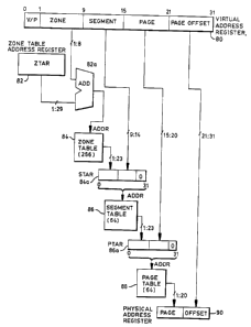
Fig. 3 is a conceptual block diagram of a virtual
address translation technique that is executed by the system
10. A virtual address register (VAR) 80 has a length of
32-bits. Bit 0 (MSB) does not form a part of the 31-bit
virtual address. Bits 1-31 are partitioned into four
fields, specifically, an 8-bit Zone, a 6-bit Segment, a
6-bit Page, and an 11-bit Offset.
Translation of virtual addresses begins with a
Zone Table Address Register (ZTAR) 82 (Fig. 4A). The ZTAR
82 is loaded by the CP 12 prior to the virtual address
translation, for example during a switch from one task to
another task. The output of the ZTAR 82 is applied to an
adder, in conjunction with the 8-bit VA Zone field, to form
a physical address which points to an entry within the Zone
Table 84 in main memory 40. The Zone Table 84 contains up
to 256 word-aligned entries (Fig. 4B), each of which points,
after being concatenated with the 6-bit VA Segment field, to
one full-word entry (Fig. 4C) of a 64 entry Segment Table
86. The Segment Table maps 8 Mbytes of virtual address
space, and is aligned on a 256-byte boundary. The output of
the Zone Table 84 is shown for convenience as being held by
a Segment Table Address Register (STAR) 84a, although in the
CA 02173225 2003-12-19
77215-11
lla
preferred embodiment of this invention no specific register
performs this function. In like manner, the output of the
Segment Table 86 points, after being
J 95/10808 ,, S;~ ~, P~ I'IL;53~;33241
12
concatenated with the 6-bit VA Page field. forms a pointer to one full-word
entry
(Fig. 4D) of a 64 entry Page Table 88. The output of the Segment Table 86 is
shown for convenience as being held by a Page Table Address Register (PTAR)
86a, although in the preferred embodiment of this invention no specific
register
performs this function. The entry of the Page Table 88 contains a 20-bit Page
number which is concatenated with the 11-bit Page Offset field to form a 31-
bit
Physical Address that is stored within a Physical Address Register (PAR) 90.
In Fig. 4A, if the MSB (designated P) is a one it is indicated that the
address is
a physical address. and ZTAR I:31 are reserved for use by the operating system
(OS). In Fig. 4B. if the MSB (designated F) is a one it is indicated that a
Zone
Fault e:~sts, and the Zone Table entry bits I:31 are reserved for use by the
OS.
The MSBs of the Segment Table Entry (Fig. 4C) and the Page Table Entry (Fig.
4D) have the same meanings, i.e., the presence of a Segment Fault and a Page
Fault, respectively. The LSBs of the Segment Table and Page Table entries
(designated M), indicate that the associated Segment or Page is monitored, and
enables the use of a specific VS Assembly Language instruction that deals with
monitored Segments and Pages. The 3-bit fields designed RRR and WWW in the
Segment Table entries and the Page Table entries indicate a Level ~0-r) of
read
protection and write protection. respectively, for the associated Segment and
Page.
The format for a CP 12 Translation Buffer (TBLTF) entry is shown in Fig. 4E.
As
in the Page Table entry, bits 21 and 30 are not used. The following conditions
apply to the setting of the M and the V bits:
WO 95/10808 PCT/US94/03241
21 ~~3~~2
13
M=0, V=1 if monitored;
1V~=1, V=0 if unmonitored; and
M=1, V=1 to fault the associated TBUF entry.
Reference is now made to Fig. 5 which illustrates a schematic diagram of the
hardware-assist logic for virtual address translation. The circuitry of Fig. ~
5 is
mostly contained within the CDU 18, and is used when the CP 12 misses on a
virtual address translation. The purpose of the hardware-assist circuitry is
to
provide an entry to the CP 12 TBUF. The TBUF is a cache capable of storing
translation information for up to 256 virtual address translations.
A decoder 92 within the CDU 18 is responsive to a plurality of bits (S) that
are
input from the micro-code control store 14. The decoder 92 is synchronized to
the
CP 12 clock and provides six control signal outputs for controlling the
hardware-
assist circuitry within the CDU 18 in response to the execution of a TRNSLA.TE
VS Assembly language instruction. The hardware-assist circuitry is controlled
to
perform the following four steps:
(1> form the address in main memory of the Zone Table Entry (ZTE) while
simultaneously checking for physical address mapping (i.e., bit 0 (P) of
ZTAR=1);
( 2 ) form the address in main memory of the Segment Table Entry ( STE ) while
simultaneously checking for a Zone fault (i.e., bit 0 (F) of ZTE=1);
( 3) form. the address in main. memory of the Pale Table Entry i PTE ) while
simultaz~eouslv checking for a Segment fault (i.e.. bit 0 (F~ of STE=1): and
(4) read the PTE into a CP 12 Translation Register (TR1) in TBUF format while
simultaneously checking for a Page fault (i.e., bit 0 (F) of PTE=1).
A fifth step loads the TBUF entry into the TBUF within the CP 12.
WO 95/10808 PCT/US94/03241
21'3225
14
More particularly, the outputs of the decoder 92 are a Load Zone Table Address
(LZTA) signal which is applied to a ZTA register 94. The application of the
LZTA
signal causes the ZTA register 94 to store 30 bits from the internal CDU 18
data
bus, the internal CDU 18 data bus being driven with the Zone Table Address
from
the DB0:31 data bus 12a by the CP 12. A second control signal is a Load
Faulted
Virtual Address (LFUVA) which is applied to a Faulted Virtual Address Register
(FUVA) 96. The application of the LFUVA signal causes the FUVA register 96 to
store 20 bits from the internal CDU 18 data bus, the 20 bits corresponding to
bits
1:20 of the faulted virtual address (the Zone, Segment, and Page fields as
shown
in Fig. 3 >.
The decoder 92 also sequentially outputs an Add Zone (ADDZ) control signal, an
Add Segment (ADDS) control signal, and an Add Page (ADDP> control signal. The
ADDZ control signal is applied as a control signal to a first multiplexer 98,
while
the ADDS and ADDP control signals are applied as control inputs to a second
multiplexer 100. The ADDP signal is also applied as a clocking input to a
Segment
Data Register (SDR) 102, which stores bits 24:31 of the Segment Table Entry
for
subsequent combination with bits 24:31 of the Page Table Entry, as described
below.
The outputs of the multiplexers 98 and 100 are applied to an adder 104 which
outputs 29 bits to an output multiplexer 106. The output of multiplexer 106 is
selectively controlled by a Report Page Table Entrv (RPTE ) control signal
that is
output by the decoder 92 aftez~ the ADDZ. ADDS az,.d the ADDP control signals.
The output of adder 104 is combined with zero bits at bit positions 00. 30,
and 31
before application to the output multiplexer 106. The output of the adder 104
( with
the zero bits at bit locations 00, 30, and 31 > is supplied from the
multiplexer 106
to the CP 12 over the DB0:31 data bus 12a. The CP 12 employs this input to
form
a physical address to first read the Zone Table Entry from main memory, then
the
Segment Table Entiy, and then the Page Table Entry. As each of these Entries
are
WO 95/10808 PCT/US94/03241
21 ~~~~5
read in turn the content of the Entrv appears on a CDU 18 internal 32-bit data
bus referred to as a Read Re-order Bus (RRB).
The second 32-bit input to the multiplexer 106 is applied from logic circuitry
that
includes a NOR function 108 and an OR function 110. The SDR 102, in
combination with the NOR function 108, the OR function 110, and the state of
bits
24:31 of the Read Re-order Bus that are conveying the. output of the PTE,
forms
the TBUF entry for the CP 12. More particularly, the outputs of the NOR
function
108 and OR function 110 are combined with bits 1:23 of the Read Re-order Bus
(RRB01:23) to provide the 32-bit data for the TBUF entry. The TBUF data entry
includes, in bit position 0, the NOR of the Segment and Page Table Entry
Monitor
bits ( derived from bit 31 of the SDR 102 and bit 31 of the RRB which is
conveying
the Page Table Entry). The TBUF data entry also includes, in bit positions
24:31,
the OR of the Segment Table Entry and the Page Table Entry RRR, yVWW, and
V bits (derived from bits 24:31 of the SDR 102 and bits 24:31 of the RRB which
is conveying the Page Table Entry).
Two input multiplexer 112 is controlled by the ADDZ control signal to output
to
the micro-code a status flag that indicates, while ADDZ is asserted, the state
of
the ZTA bit 0 (P), and while ADDS, ADDP, and RPTE are asserted the state of
the
RRB bus bit 0 (the Fault indicator for the Zone Table Entry, the Segment Table
Entry, and the Page Table Entry, respectively). This status flag is tested by
the
micro-code and is acted on as follows.
If P=1 in. the Zone Table Address Re~iste?- ( 7TAR ~. them ma.p the TBUF entrv
as
virtual=physical and terminate the virtual address translation operation.
If either the Zone, Segment, or Page is faulted (F=1), then store the faulted
virtual
address at a predetermined location, and branch to generate a program
exception.
This effectively terminates the virtual address translation operation.
WO 95/10808 PCTIUS94/03241
16
With respect to the adder 104, the following operations are performed (it is
assumed that the LZTA signal has been previously asserted to load the ZTA
register 94 ). After a first micro-code instruction asserts the LFWA control
signal,
and loads the FUVA register 96, a next micro-code instruction generates the
ADDZ control signal. This causes the multiplexer 98 to select bits 01:29 from
the
ZTA 94, and the multiplexer 100 to select bits 01:08 (Zone field) from the
faulted
virtual address stored in FUVA 96. The adder 104 thin adds the Zone field to
the
contents of the ZTAR 82. The output of the adder 104 is combined with zeros at
bit positions 00, 30, and 31 and is applied, via multiplexer 106, to the CP
12. The
CP 12 receives this data input and stores same in a Physical Address Register
(PAR) for subsequent application, during a next micro-code instruction, as a
physical address on PA bus 12b to read one entry of the Zone Table 84 within
main memory 40 (or cache 16). The selected entry appears on the RRB of the
CDU 18 during the next micro-code instruction.
In response to the next micro-code instruction, the physical address is
applied to
the memory to read the selected entry of the Zone Table 84 and the decoder 92
deasserts the ADDZ control signal and asserts the ADDS control signal. This
causes the multiplexer 98 to select bits 1:23 of the RRB, along with zeros on
bits
24:29, and the multiplexer 100 to select bits 09:14 (Segment field) from the
faulted
virtual address stored in FUVA 96. The adder 104 then adds the Segment field
(appearing on bits 24:29) to the zeros appearing on bits 24:29 of the RRB Zone
Table Entry data. This effectively concatenates the Segment field to bits 1:23
of
the Zone Table Entry, as depicted in Fig. 3. The output of the adder 104 is
again
selectivel.v combined with zero bits and. applied. to the CF 12. As before,
the CP
12 stores this data as a phvsic~l address in. the FAR to access, during a next
micro-code instruction, one entry of the Segment 'fable g6 within the main
memory 40.
In response to the next micro-code instruction the physical address is applied
from
the PAR to the memory to read the selected entry of the Segment Table 86, and
WO 95/10808 PCT/US94/(13241
~;73;~~5~
17
the decoder 92 deasserts the ADDS control signal and asserts the ADDP control
signal. This causes bits 1:23 from the Segment Table Entry (appearing on
RRB01:23> to be concatenated, via adder 104, with bits 15:20 (Page Field> of
the
faulted virtual address. The output of the adder 104 is selectively combined
with
zeros and is applied via multiplexer 106 to the CP 12. The CP 12 stores this
data
as a physical address in the PAR to access, during a next micro-code
instruction,
one entry of the Page Table 88 within the main memory.
At the time that the ADDP control signal is asserted the portion of the
selected
Segment Table entry that appears on bits 24:31 of the RRB are latched into the
SDR 102. The output of the SDR 102 is subsequently selectively combined during
the next micro-code instruction with the data appearing on the RRB from the
selected Page Table Entry (with NOR 108 and OR 110) and is concatenated with
bits 01:23 of the Page Table Entry appearing on RRB01:23. This provides a 32-
bit
TBUF Entry that is output to the CP 12 from multiplexer 106 by the assertion
of
the RPTE control signal during this micro-code instruction.
As it was indicated above, simultaneously with the generation of the physical
addresses for the Zone Table, Segment Table, and Page Table the multiplexer
112
is providing status information to reflect the status of the P and F bits of
the Zone
Table Address Register and the Zone, Segment and Page Table Entries,
respectively.
This invention thus provides an efficient and rapid method to update the TBUF'
entry within the CP 12 in response t.o the occurrence o.f. a fa~ilted virtual
addrecc.
while also providing indication;: of. th.e presence of a. pb.vsicai address
within the
ZTAR 82 or the presence of a faulted Zone. Segment, or Page Table entry.
As was indicated previously, before the implementation of the circuitry and
method of this invention as many as 22 micro-code instructions were required
to
update the TBUF, whereas the use of the invention requires a total of but nine
J 9110808 W T,LSS.lJ03291
_ 1g
micro-code instn.~.ctions. This yields a significant improvement in execution
time.
and frees a significant number of locations within the control store 14.