Language selection

Search

Patent 2173367 Summary

Third-party information liability

Some of the information on this Web page has been provided by external sources. The Government of Canada is not responsible for the accuracy, reliability or currency of the information supplied by external sources. Users wishing to rely upon this information should consult directly with the source of the information. Content provided by external sources is not subject to official languages, privacy and accessibility requirements.

Claims and Abstract availability

Any discrepancies in the text and image of the Claims and Abstract are due to differing posting times. Text of the Claims and Abstract are posted:

  • At the time the application is open to public inspection;
  • At the time of issue of the patent (grant).
(12) Patent: (11) CA 2173367
(54) English Title: PROTECTION SWITCHING APPARATUS AND METHOD
(54) French Title: PROCEDE ET APPAREIL DE COMMUTATION DE SECOURS
Status: Deemed expired
Bibliographic Data
(51) International Patent Classification (IPC):
  • H04Q 1/22 (2006.01)
  • G06F 11/00 (2006.01)
  • G06F 11/20 (2006.01)
  • H04B 1/74 (2006.01)
  • H04L 1/22 (2006.01)
  • H05K 10/00 (2006.01)
(72) Inventors :
  • OPOCZYNSKI, ADAM (United States of America)
(73) Owners :
  • ADC TELECOMMUNICATIONS, INC. (United States of America)
(71) Applicants :
(74) Agent: GOWLING WLG (CANADA) LLP
(74) Associate agent:
(45) Issued: 1999-09-07
(86) PCT Filing Date: 1994-10-04
(87) Open to Public Inspection: 1995-04-13
Examination requested: 1996-04-02
Availability of licence: N/A
(25) Language of filing: English

Patent Cooperation Treaty (PCT): Yes
(86) PCT Filing Number: PCT/US1994/011266
(87) International Publication Number: WO1995/010146
(85) National Entry: 1996-04-02

(30) Application Priority Data:
Application No. Country/Territory Date
08/133,741 United States of America 1993-10-07

Abstracts

English Abstract


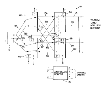
A protection switching system (10) includes a plurality of telecommunications modules (12, 14A. 14B, 16A, 16B) for processing
and/or switching telecommunications signals. A first module (12) provides signals to one pair of modules (12A, 12B), which are in turn
connected to another pair of modules (16A, 16B). A standby module (14B, 16B) controls the switching of all the modules (12, 14A, 14B,
16A, 16B) in the system (10) which require switching in the event that a standby module (14B, 16B) is activated. A controller monitor
circuit (20) monitors the faults present on the working modules (14A, 16A) and, if a fault is detected, signals the corresponding standby
module (14B, 16B), which in turn provides protection switching.


French Abstract

Un système de commutation de secours (10) comprend une pluralité de modules de télécommunications (12, 14A, 14B, 16A, 16B) permettant de traiter et/ou de commuter des signaux de télécommunications. Un premier module (12) fournit des signaux à une paire de modules (12A, 12B) qui sont à leur tour connectés à une autre paire de modules (16A, 16B). Un module de réserve (14B, 16B) commande la commutation de tous les modules (12, 14A, 14B, 16A, 16B) du système (10) qui requièrent une commutation dans l'éventualité où un module de réserve (14B, 16B) serait activé. Un circuit de surveillance/commande (20) surveille les anomalies présentes sur les modules en service (14A, 16A), et, si une anomalie est détectée, la signale au module de réserve correspondant (14B, 16B), qui effectue à son tour une commutation de protection.

Claims

Note: Claims are shown in the official language in which they were submitted.


5


What is claimed:
1. A protection switching system, comprising:
a first stage module having an input and output;
a pair of second stage modules, each second stage module having an
input and output for connection to the first stage module for transmission and
reception of signals therebetween, one of said second stage modules being a
working module, the other of said second stage modules being a standby
module;
a pair of third stage modules, each third stage module having an input
and output for connection to an input and output of each of said second stage
modules for transmission and reception of signals therebetween, one of said
third
stage modules being a working module, the other of said third stage modules
being a standby module;
a controller/monitor circuit to monitor fault conditions of the working
modules and to issue a control signal upon detection of a fault condition in a
working module to cause at least one of the standby modules of the second and
third stage standby modules to function in place of the working module in
which
a fault condition is detected; and
the at least one standby module of the second and third stage standby
modules includes means for switching the inputs of the first stage module,
standby modules, and working modules, to a standby position corresponding to
an activation of the at least one standby module.

Description

Note: Descriptions are shown in the official language in which they were submitted.


~wo 95/10146 ~ 3 3 6 7 PCT~US91/11266


PRC~CIION S~~ G APPARATUS AND Mh'IHOD

Technical Field of the Invention
The present invention pertains to protection switching in a
telecommunication system.

E3ackground of the Invention
Telecommunication and other systems somptim~s require that
backup equipment be switched into operation within a short period of time
after a failure is (1etecte~1 in the primary equipment.

Summary of the Invention
The present invention provides a~lus and method for
rapidly switching backup equipment into operation. According to the
invention, a controller/mnnitor processor monitnr~ the status of a plurality of
telecommunications circuit module pairs, each pair having a working module
and a standby module. Each standby module includes means operative upon a
20 signal from the processor for switching all other module inputs in the systemwhich require reconfiguration due to the activation of the standby module.

~rief Description of the ~rawings
Figure 1 is a simplified block diagram of the protection
25 switching system of the present invention;
Figure 2 is a simplified block diagram of one failure mode and
corresponding protection switching operation, according to the present
invention; and
Figure 3 is a simplified block diagram of another failure mode
3 o and the corresponding protection switching, according to the present invention.

Detailed Description of the Invention
Referring now to Figure 1, the protection switching system of
the present invention is illustrated. System 10 is illustrated in a

WO 9~/101~6 PCT/US9~/11266
~1733~7


telecommunications system, wherein a first telecommunications module l is
connected to a pair of modules 14A and 14B. 14A is the working module.
and norrnally is connected to module 12 such that module 12 conveys signals
along path 13A to module 14A and such that module 12 receives si~nals
5 along path 13B from module 14A. Paths 13A and 13B, as in the case of all
other paths in the system, may comprise, for e~ample, an electronic circuit
connection, a wired connection, or a fiber optic connection. Module 14B
serves as a backup to module 14A.
A further pair of modules 16A and 16B are connected to
10 modules 14A and 14B. Module 16A serves as the working module, with
module 16B as the standby. In norrnal operation, module 16A receives
signals from module 14A along path lSA. Module 16A provides signals bacl~
to module 14A along path 15B. Module 16A outputs signals along path 17A
and receives signals along path 17B. Paths 17A and 17B may be connected
15 to other equipment or to a telecommunications network.
Each of modules 12, 14A, 14B, 16A and I6B are simplified
representations of electronic circuit modules which receive signals and process
and/or switch those signals. The function of a module is not important to the
invention. The modules ll~mil and switch signals in both directions. For
20 the purpose of this description, modules 14A and 14B may be considered
second stage modules, and modules 16A and 16B third-stage modules.
Module 12 may be termed a first stage module. Modules 14B and 16B
initially serve as standby to modules 14A and 16A respectively. However,
when the standby unit is activated, it becomes the working unit and the other
25 becomes the standby (once replaced and operating again). Module 14B is
normally switched to receive input from path 13C from module 12~ and apply
its output to the disconnected inputs of modules 16A and 16B over the
respective paths lSE and 15G. Module 14B is also connected to apply an
output on path 13D to the disconnected output of module 12. Module 14B
3 o f~her receives an input over path lSF to its normally cnnn~cted input and an input from path lSH to a normally disconnPcte~ input.

~ WO 9SI10146 ~ 3 ~ ~ 7 PCT/US9~111266


Path lSC connects an output of module 14A to the normally
connected input of module 16B, while the path lSD connects an output of
module 16B to the normally disconnected input of module 14A.
Modules 14A, 14B, 16A and 16B each include fault detection
5 circuitry for cletectin~ the occurrence of errors or fault conditions in the
circuitry. This circuitry is shown as the dashed line box with the "F" label
and produces fault signals "F" that are output from the modules.
Controller/monitor circuit 20 monitors the errors or fault signals generated by
modules 14A, 14B, 16A and 16B carried over one or more lines from the
10 modules to the controller/monitor circuit 20.
In the event a fault condition is ~l~tectçd in a working module
14A, controller/monitor circuit 20 sends a control signal "C" to the control
input "C" of module 14B. A switching control circuit shown as a dashed line
box with the label "C" in module 14B then controls the switching of module
15 12 and module 16A and 16B to the "standby" positions. The control of
modules 12 and 16A and 16B is diagrammatically illustrated by control line
30. Figure 2 illustrates the position of the various switches and signal paths
after module 14B is switched into operation and module 14A is disabled.
In the event that controller/monit~-r 20 detects an error or fault
20 condition in a working module 16A, it sends a control signal to standby
module 16B (also having a switching control circuit), which in turn, using
control line 40, switches modules 14A and 14B to provide the configuration
shown in Figure 3. Module 16B thus becomes the working module, and 16A
the standby. In norrnal operation, the output of module 16B is disc~ nnect~l,
25 such that it does not produce an active output signal on path 17C. Upon the
receipt of a control signal for monitor/controller 20, the inputs and outputs ofmodule 16B are switched to provide an active output on output 17C. All
, modules in the system are norrnally operating to switch or process signals.
Thus, if modules 14A and 14B are fully operational and receiving the sane
3 o signals, they are producing identical output signals. The same is true for
modules 16A and 16B. This allows the operation of the modules to be
compared to one another to determine if a fault condition has occurred in one.

WO 95/10146 2 I PCTIUS9-1/11266 ~
. 7~3~7


Also, it allows switching to occur sllbst~nti~lly in~t~nt~neously, as only the
inputs need be switched to take signal from a different module. Thus~ to
reiterate, when ~h~n ing configurations, only the inputs of modules 1~ 14A~
14B, 16A or 16B are switched, and the outputs of 16A and 16B are enabled
5 or conn~.ct~l, as the case may be.
When module 14B or 16B is the working module, it also
conkols switching back to the other module in the pair, and the associated
input switches, reverse of the switching described above. If a module 14B or
16B is removed or disabled, switching ~lltom~tically defaults to inputs applied
10 to modules 14A or 16A, as the case may be.
Thus, as described above, the present invention provides a
system wherein the standby module 14B or 16B, once activated, controls the
switching of other modules receiving signals from the standby module to
reconfigure as nece.e~ry to obtain swift standby operation, so that telephone
15 service is not noticeably interrupted.
As it shall be readily appreciated, system 10 can be extended to
include additional source, ~ll~n and/or downstream modules.

Representative Drawing
A single figure which represents the drawing illustrating the invention.
Administrative Status

For a clearer understanding of the status of the application/patent presented on this page, the site Disclaimer , as well as the definitions for Patent , Administrative Status , Maintenance Fee  and Payment History  should be consulted.

Administrative Status

Title Date
Forecasted Issue Date 1999-09-07
(86) PCT Filing Date 1994-10-04
(87) PCT Publication Date 1995-04-13
(85) National Entry 1996-04-02
Examination Requested 1996-04-02
(45) Issued 1999-09-07
Deemed Expired 2002-10-04

Abandonment History

There is no abandonment history.

Payment History

Fee Type Anniversary Year Due Date Amount Paid Paid Date
Application Fee $0.00 1996-04-02
Registration of a document - section 124 $0.00 1996-06-27
Maintenance Fee - Application - New Act 2 1996-10-04 $100.00 1996-09-13
Maintenance Fee - Application - New Act 3 1997-10-06 $100.00 1997-09-17
Maintenance Fee - Application - New Act 4 1998-10-05 $100.00 1998-09-17
Final Fee $300.00 1999-06-02
Maintenance Fee - Patent - New Act 5 1999-10-04 $150.00 1999-09-20
Maintenance Fee - Patent - New Act 6 2000-10-04 $350.00 2000-10-19
Owners on Record

Note: Records showing the ownership history in alphabetical order.

Current Owners on Record
ADC TELECOMMUNICATIONS, INC.
Past Owners on Record
OPOCZYNSKI, ADAM
Past Owners that do not appear in the "Owners on Record" listing will appear in other documentation within the application.
Documents

To view selected files, please enter reCAPTCHA code :


To view images, click a link in the Document Description column. To download the documents, select one or more checkboxes in the first column and then click the "Download Selected in PDF format (Zip Archive)" or the "Download Selected as Single PDF" button.

List of published and non-published patent-specific documents on the CPD .

If you have any difficulty accessing content, you can call the Client Service Centre at 1-866-997-1936 or send them an e-mail at CIPO Client Service Centre.


Document
Description 
Date
(yyyy-mm-dd) 
Number of pages   Size of Image (KB) 
Claims 1998-12-30 1 35
Representative Drawing 1999-08-31 1 9
Representative Drawing 1997-06-16 1 9
Cover Page 1996-07-15 1 17
Abstract 1995-04-13 1 50
Description 1995-04-13 4 185
Claims 1995-04-13 1 36
Drawings 1995-04-13 3 45
Cover Page 1999-08-31 1 52
Prosecution-Amendment 1999-01-05 1 29
Correspondence 1999-06-02 1 28
Fees 1996-09-13 1 63
Prosecution Correspondence 1996-04-02 6 241
Prosecution Correspondence 1996-04-02 1 23
Examiner Requisition 1998-09-15 2 61
Prosecution Correspondence 1998-12-14 1 34
International Preliminary Examination Report 1996-04-02 6 203
National Entry Request 1996-04-02 7 234