Note: Descriptions are shown in the official language in which they were submitted.
217~~64
a
10
1 5 METHOD OF AND DEVICE FOR MEASURING THE REFRACTIVE INDEX OF WAFERS OF
VITREOUS MATERIAL
The invention described herein relates to methods of measuring the
refractive index and in particular concerns a method and a device for
2 0 determining the refractive index of a wafer of vitreous material.
Preferably) but not exclusively, the invention is employed in measuring
the refractive index in a limited area (about 1 mm2) of a thin sample of an
optical fibre preform of fluoride glass.
It is well known that the refractive index of a body of a fluoride glass,
2 5 such as an optical fibre preform, depends not only on the composition of
the
glass but also on its thermal history: in effect) during the casting and
drawing processes stresses or dishomogeneities may arise which give rise to
local fluctuations in the refractive index) which fluctuations must be
detected
and eliminated.
3 0 The conventional devices for measuring the refractive index of samples
of transparent material, which are based on measuring the limit angle (for
instance Pulfrich refractometers) require sending a grazing beam onto the
sample and analysing the beam refracted by the sample. These devices cannot
be employed to measure directly the refractive index of the core and the
3 5 cladding of an optical fibre, since the size of the sample is too small to
obtain
a significant amount of refracted light. Using a Pulfrich refractometer for
measurements on a glass sample whose composition is analogous to that of the
preform) on the other hand, does not allow taking into account the thermal
21 ~3~~~
history of the glass, and in particular the fact that the cooling conditions
of a
wafer are different from those of a cylindrical body like the preform.
European patent EP-B 0 085 978, in the name of the same applicant,
describes a method of determining the refractive index, which method can
also be employed in the case of small samples) such as those obtained by
cutting an optical fibre preform. According to the known method, the sample
is placed on a support which can be rotated; a light beam comprising two
monochromatic radiations is sent towards the sample with a first angle of
incidence and the two radiations are made to interfere upon leaving the
sample, thereby creating a first beat; subsequently, the support is rotated)
the
beam is sent on the sample with a second angle of incidence and the two
radiations are again made to interfere upon leaving the sample, thereby
creating a second beat. The refractive index is obtained from the phase
differences between the two beats and a reference beat obtained by making
the two radiations of the beam interfere at the end of a path external to the
sample.
However, radiations which pass through the sample inevitably undergo
multiple reflections inside it, and these bring about interference phenomena
which result into a phase error limiting the accuracy of the measurement to
2 0 such an extent that it is no longer possible to appreciate said
fluctuations in
the refractive index. Moreover, the measurement is quite sensitive to thermal
expansion and to electrical drift.
A more detailed analysis of the disturbance caused by multiple
reflections, carried out by the inventor in order to correct or in any case to
2 5 take into account errors stemming from such disturbance, has yielded the
surprising result that it is possible to exploit the disturbance itself to
obtain
an accurate measurement of the refractive index. The object of the invention
is thus to provide a method and a device which exploit interference
phenomena due to multiple reflections inside the sample.
3 0 According to the invention a method is provided in which a source
generates a light beam which is sent towards the wafer at different angles of
incidence and the intensity of a beam transmitted by the wafer is measured as
the angle of incidence varies, and in which: the beam generated by the
source is a coherent monochromatic beam whose coherence length exceeds
3 S the thickness of the wafer; said beam, before being sent towards the
wafer, is
transformed into a collimated beam with plane wave front) in order to give
rise to fluctuations of the wafer transmittance as the angle of incidence
varies, because of the interference due to multiple reflections of the beam
CA 02173564 1999-07-21
.. 3
inside the wafer; the values of the wafer transmittance are obtained from the
measured values of the intensity; the angular positions of the transmittance
maxima and minima are determined) within a preset range of angles of
incidence) with respect to a maximum or a minimum corresponding to normal
incidence) and the refractive index is obtained from these positions and from
the number of maxima and minima in the different angles.
The invention also concers the device performing the method.
For the sake of further clarification, reference is made to the enclosed
drawings, where:
- Figure i is a schematic diagram of the device performing the method;
- Figure 2 is a diagram of the transmittance versus the angle of incidence)
for a range of angles at the two sides of normal incidence;
- Figure 3 are diagrams of the transmittance versus the cosine of the angle
of incidence and of a second curve) used to determine the positions of
transmittance maxima and minima;
- Figure 4 is a diagram plotting the cumber of transmittance maxima and
minima determined using the curves in Figure 3, versus the angle of
incidcnce,as well as the trend of a theoretical function linked to that
number; and
2 0 - Figure 5 is a flow chart illustrating the operations of the method
according to the invention.
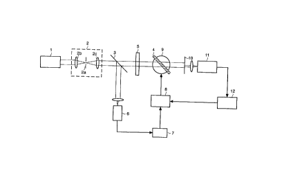
In Figure 1) a source 1) e.g. a He-Ne laser, generates a beam of coherent
monochromatic light. A spatial filter 2) comprising a pinhole diaphragm 2a
placed between a first lens 2b) which focuses the beam emitted by the source
2 5 onto the pinhole, and a second lens 2c, which collimates and expands the
beam exiting the diaphragm) generates a beam with plane wave front. The
collimated beam is split into two fractions by means of a beam splitter 3. A
first fraction is sent towards a sample 4) which is a wafer with plane and
parallel faces whose thickness is smaller than the coherence length of
3 0 source I. Said beam fraction passes through a polariser 5 which orients
the
polarisation plane of the beam fraction in such . a way that the
electrmnagnetic
field is parallel to the angle of incidence (S wave).
Inside the sample) the beam undergoes multiple reflections and) due to
the characteristics of the beam) there are noticeable fluctuations in the
3 5 transmittance of the sample as an effect of interference between the
various
reflected beams. These fluctuations are exploited to determine refractive
index. The particular choice of the polarisation makes the measurements easy
since the amplitude of the fluctuations is larger in the case of S wave.
2~7~~~~
The second beam fraction is sent directly to a reference detector 6 whose
output signals are provided to an analogue-to-digital converter 7 connected to
a processor 8.
Sample 4 is mounted on a motorised support 9 which can be rotated
under the control of processor 8 to vary the angle of incidence of the beam
on sample 4. The support is associated to an extremely accurate angular
position detector, in particular an encoder with the ability to provide the
position of the support with an accuracy on the order of tenths of a second of
a degree. For the sake of simplicity, in the drawing the motor and the encoder
are incorporated in support 9. The beam exiting sample 4 passes through a
movable diaphragm 10 which allows selection of the area of the sample on
which the measurement is to be performed) and it is collected by a second
detector 11 followed by an analogue-to-digital converter 12 connected to
processor 8.
Processor 8 receives, from converters 7 and 12, current or voltage
values representing the intensities of the reference beam and of the beam
transmitted by wafer 4 (which is proportional to transmittance) as the angle
of incidence varies, and computes the ratio of said values, associating the
values of that ratio to the angular position of the support. Note that the
2 0 intensity of the transmitted beam only could be used for processing;
however,
as shall be better shown further on) the actual value of transmittance is not
of interest for the invention and using the ratio between the two intensities
allows the effects of noise to be reduced. Assuming that support 9 is rotated
in
a range from +45° to -45° with respect to normal incidence,
sufficient data
2 5 for subsequent processing are obtained by rotating support 9 in steps of a
few
tens of seconds of a degree.
Figure 2 shows the transmittance versus the angle of incidence (in
degrees) for a small range of angles on the two sides of normal incidence. The
values of the ordinates are not indicated) since they depend on the measured
3 0 quantity (intensity of the beam transmitted by the sample or ratio between
transmitted beam and reference beam intensities). The Figure clearly depicts
transmittance fluctuations due to interference phenomena caused by
multiple reflections inside wafer 4, and shows that oscillation frequency
increases as the angle of incidence increases. According to the invention, the
3 5 refractive index is obtained by identifying the positions of maxima and
minima of the curve in Figure 2 with respect to the position of normal
incidence (0 in the Figure) and the number of maxima and minima
corresponding to the various rotation steps: this number, as will be shown
2i7~5d4
further on, can be expressed, for a given thickness of the sample and a given
wavelength of the radiation used, as a function of refractive index and angle
of incidence. The position of normal incidence is in turn accurately
determined by identifying first the approximate point around which the
S curve is symmetrical) then two maxima or minima which are symmetrical
with respect to that point and finally by choosing as angle 0 the intermediate
value between the two considered maxima and minima. The operation is made
easier by the oscillation frequency being relatively low near normal
incidence.
1 ~ For processing) the positions of transmittance maxima and minima are
used in place of the actual values because the position is much less sensitive
to errors due to drifts or to the state of cleanliness or finish of the faces
of the
sample. Greater processing complexity is counterbalanced by the
improvement in accuracy.
15 To determine the positions of maxima and minima, intervals containing
each one maximum and one minimum are looked for in the curve. For this
purpose, a function P(8 ) (for instance) a straight line or a curve
corresponding to a second degree polynomial function with a very small
coefficient of the second degree term) is determined from the data, which
2 0 function intersects the peaks in Figure 2 essentially at mid height, and
the
values of 8 corresponding to the intersections between the two curves are
identified. Operations are simplified if both T and P are expressed as a
function of cos8 , since peaks in function T(cos8 ) are essentially equally
spaced, as Figure 3 shows. For the sake of simplicity, a function of the type
2 5 P ( c o s 8 ) = constant was considered for curve P in the drawing.
Intersection
points between P and T are those for which, in the points of the two curves P,
T corresponding to two successive positions of sample 4, relation
(Ti _ Pi).(Ti_1 _ Pi_ 1 ) ( 1 )
applies) and moreover the distance between the previous point in which
3 0 relation (1) has been met and the current point exceeds a given value
(e.g.
the distance between successive peaks) so as to eliminate spurious
intersection points due to noise. Once the intervals have been determined, it
is sufficient to approximate the experimental curve in each interval with a
polynomial of at least the 3rd degree and to determine analytically the
3 5 maximum and minimum thereof. The refractive index is then obtained from
the angular positions 8 g of the maxima and minima of T and from the overall
number Vg of the maxima and minima present in the interval 0 - Ag.
CA 02173564 1999-07-21
b
The following description provides a brief outline of the theory on
which the method according to the invention is based.
Considering sample 5 as a mufti-layer) transmittance T can be expressed
as a function of angle of incidence 8 , wavelength ~, of the incident
radiation)
refractive index n and thickness d according to the following relation:
T(e~n~d~~) = 1 4~- l
C(9,n)+D(9,n)~cos ~ ~d~n~N(8,n)~
where
N(6,n)= 1-sin26/n2 (3)
1 1 cos 9 n ~ N(8) n) cos 8 2
C(9,n) _- - +1 + +1 (4)
4 ~ 2 ~ n~N(9,n) 2cos8 n~N(B,n)
2
D(9,n)= 1 1_ 1 cos8 +1 _ n~N(9,n) 1_ 1 cos8 +1
4 ~ 2 ~ n~N(9,n) cosh 2 ~ n~N(9,n) (5)
The relations are
above obtained
by
applying
the
principles
described
for example in and
"Theory calculations
of
optical
thin
films",
by
P.
H.
i S Berning) films)
Physics of thin Vol.
1
pages
69
and
fol.
To
identify
the
positions of
the maxima and
minima of T
as a function
of 8 it will
be enough to
compute the derivative T
of with
respect
to
8
and
to
set
it
to
0.
The
result
is
a
relation of the
type:
aD(8,n)
i +
t
4
N
9
d
s arc N(g;n)
n ~n~
(
,n)
~n~
-~4~n~d
~n~
ae
(6)
aC(B,n)
_ a-.
aD(9,n) 2 aN(B,n) 2
~ + 4~ n-d
~n.
,
~
ae ae
2 0 It can be
verified that)
for refractive
index values
typical of vitreous
materials (in 2))
particular < thicknesses
of
few
millimetres
and
wavelengths
in the visible in
spectrum, the
range
of
angles
under
consideration
the
second member (6)
of relation is
very
small
(<
0.001)
and
therefore
the
sine
at
the first member considered
can be equal
to
its
argument.
Therefore,
relation
2 5 (6) is equal argument
to 0 when the of
the
sine
is
equal
to
mn,
i.e.
when
CA 02173564 1999-07-21
., . . ~ 7
aD(8, n)
m =4~d~n~N(8,n)+ ~arct a~ (7
1~~~~d~n~ a8
Now) let us consider the function:
aD(O, n)
F(9,n,d,~.)= ~ ~d~ n~N(O,n)+ ~arctg N(O,n)
-4~~c~d~n~
ae (g)
aD(6) n)
-~ .d.n~N(8,n)- ~arct .~
--4 . tt. d . n a8
This function is equal to 0 for 8 = 0 and can be interpreted) when it has
an integer value) as the overall number of maxima and minima of T.
Moreover, its trend is very similar to that of the curve obtaiaed by plotting
number V of maxima and minima of T) determined in the way described
above, versus B . This similarity can clearly be seen in Figure 4) where the
solid line corresponds to the aforesaid plot and the dashed line to curve (8).
1 0 The trend of curve (8) . varies abruptly even for small variations of a:
however) if for each value of a one of the two curves is translated vertically
so that it intersects the other in one point) the difference between the two
curves) in the range of angles under consideration, is negligible (< 109). The
value of ~ that minimises the differences between curve (8) and the
experimental data in the range of angles under consideration shall be the
value of the refractive index of the sample.
To obtain satisfactory results it is necessary to take some measures)
which allow minimising the effects of the error due to the inaccuracy in the
knowledge of thickness ~ and taking into account only the shape of the curve
2 0 F and not the position.
To take into account the shape of the curve, one can consider the
difference between the value of F and the experimental value for a first
angle 8 R which can be the angle of normal incidence or the angle
corresponding to one of the first peaks of the curve in Figure 2. The effect
of
2 5 thickness d can be minimised by normalising both V and function F (already
corrected to take into account the shape difference) with respect to the value
corresponding to a second angle 8 g) for example an angle near the last peak.
In practice, denoting by Vg ) VR, Vg the number of maxima and minima in
correspondence with a generic angle A g and respectively with angles 8 R and
3 0 A g) and by N the total number of maxima and minima determined
s 217364
experimentally, the refractive index can be determined by minimising
function
2
M(n~~.~d)=~ VK_VR _F(9x~n~d~~.)_F~9R,n~d~~,) (9)
R=1 VF VR F(BFv72,d,~)_F(BR,il,d,~)
The accuracy in measuring n can be further improved by using in
relation (6), instead of VR, Vg, values obtained through interpolation) with a
second degree curve) of a preset number of previous and subsequent values)
for example 50.
The operations described above are also reported in the flow chart in
Figure 5.
The system just described does not require the creation of a beat between
beams following different paths, so clearly it is immune to disturbances) such
as thermal expansion in the components of the device, which cause
variations in the optical path (aside from possible expansions of the wafer,
which in any case are negligible with respect to those of the external
components). Exploiting the number of transmittance maxima and minima
and not their values, moreover, renders the system immune to electrical
drifts.