Note: Descriptions are shown in the official language in which they were submitted.
~:~ 7427~
COMBINATION CONNECTOR
BACKGROUND OF THE INVENTION
1. Field of the Invention
The invention relates to electrical connectors, and in
particular to electrical connectors of the type used to couple data
communications cables with circuitry on a network or communications
10 interface card.
2. Description of Related Art
An RJ-45 connector in which an indicator light is included
within the connector housing is known from US Patent No. 4,978,317.
15 One of the embodiments of the invention disclosed herein involves a
similar use of an indicator light, namely in a combination connector of the
type first described in US Patent No. 5,401,192, from which priority of
the present application under 35 USC 120 is claimed. The indicator
light embodiment is one of several embodiments disclosed in this
20 application, all of which have to do with combination connectors
2 ~ 3
designed for use on computer interface cards, and is the only one not
disclosed in the related priority applications.
The demand for cables and connectors capable of
5 transferring data between computers and peripherals has increased
exponentially in recent years as the advantages of networked systems of
personal computers, and access to the so-called information highway,
have become increasingly evident to users. Despite the increasing
popularity of modem communications and networked computer systems,
10 however, and the corresponding tendency towards standardization of
system components, there currently exists a wide variety of different
cable and connector types, with none likely to attain exclusivity in the
foreseeable future. The different cable types currently in widespread use
include twisted pair cables and coaxial cables for serial communications,
15 and numerous different multiple wire configurations for parallel
communications.
In general, twisted pair cables are coupled to a network or
data communications interface via connectors of the type popularly
20 referred to as modular phone jack connectors because of their
resemblance to the standard four wire telephone jack connector. This
type of connector is commonly denoted by the letters RJ, followed by a
numerical indicator (e.g., the RJ 45 connector often used in Ethernet
applications). An example of a state-of-the-art modular jack connector
~7~273
with advanced filtering capabilities is found in copending U.S. Patent
Application Serial Number 08/043,544.
Coaxial cable connections are usually accomplished by a
5 type of connector known as the BNC connector. An example of a state-
of-the-art BNC connector with advanced filtering capabilities is shown in
copending U.S. Patent Application Serial Number 08/075,876.
Multiple wire cables, on the other hand, utilize a variety of
10 different multiple pin connectors, including mini-DlN connectors and D-
sub connectors such as the RS-232 standard 25 pin (DB25) connector, or
the 15 pin (DB15) connector commonly used in Ethernet cards.
Depending on the specific needs of the user, these connectors may be
either shielded or unshielded, and may or may not include filter
15 components such as capacitors.
Although each different cable type requires a different
connector, the use of separate interface cards for each type of cable or
connector is unnecessarily redundant, and thus it is common to provide
20 more than one type of connector on a single card in order to enable the
card to communicate with compatible devices which differ only in the
choice of cable or connector required. The Ethernet network interface,
for example, can interchangeably use all three of the above-mentioned
types of cable and thus, in order to provide compatibility with a maximum
~1 ~4~7~
number of external devices, it is common to provide as many as three
different types of connectors on a single Ethernet interface or adapter
card .
Fortunately for interface card manufacturers, the three most
common types of connectors-modular jack connectors, BNC connectors,
and D-sub parallel connectors are small enough to fit side-by-side on a
standard network card. Conventionally, this is accomplished without
modifying the connectors. However, it turns out, for reasons which were
10 not previously appreciated by those skilled in the art, that placement of
the three standard connectors on a card without modification is a less
than optimal configuration.
The first reason why it is disadvantageous to place multiple
15 connectors on a single card without modification of the connectors has to
do with the cost of the circuit board on which the connectors are placed.
This cost, previously ignored by connector designers, is significant. Even
though the space occupied by multiple connectors placed side-by-side on
an interface card may be acceptable from the standpoint of compatibility
20 with available slots in the device within which the card is to be used, this
space necessitates a larger board than might otherwise be required. Even
small decreases in the total footprint of the connectors can result in
significant savings in materials costs. For example, printed circuit board
materials presently cost approximately $.12 per square inch. This is a
21~4273
very high cost when one considers the volume of cards sold and the
overall price of each card, and thus it would be very desirable to reduce
the size of the card as much as possible. A reduction in width of one half
inch for a typical eight inch interface card saves, at approximately $.48 in
5 material costs per card.
The second reason why placement of multiple connectors on
a card without modification is less than optimal is that the provision of
multiple connectors on a card results in redundancies, previously
10 unrecognized, which could be eliminated by sharing certain components
between connectors, in particular housings, shielding, and the board locks
used to mount the connectors on the card.
The connectors described in the above-mentioned U.S.
15 Patent No. 5,401,192 and copending U.S. Patent Application Serial No.
08/252,425 solve the problems of reducing card height and sharing
components by providing components for combinations of the modular
jack, BNC, and D-Sub connectors in a single molded housing, and by
providing a common shield for the respective connectors. Despite this
20 optimal use of connector components, however, a demand exists for one
additional improvement described herein, namely the inclusion of indicator
lights. Conventionally, indicator lights are provided separately from any
connectors on the circuit card, but in situations where a combination
connector is desirable, the inclusion of indicator lights in the connector
2174~ ~3
itself would also be desirable as a space saving measure. The indicator
light described in this continuation-in-part application is designed to be
used for test purposes, providing an easy visual reference for enabling the
tester of a circuit card to test the operation of circuits on the card,
5 although those skilled in the appreciate that the indicator light described
herein can also be used as a status indicator during normal operation of
the card.
SUMMARY OF THE INVENTION
It is accordingly a first objective of the invention to provide a
connector configuration for a circuit board or card which requires less
space than conventional configurations, and which may further include an
indicator light.
It is a second objective of the invention to provide a
connector configuration for a circuit card in which redundancy is
eliminated by sharing components between the connectors.
It is a third objective of the invention to provide a combined
20 modular jack and BNC connector having an indicator light for use on a
circuit card.
It is a fourth objective of the invention to provide a single
connector configuration for a circuit card capable of providing modular
~ 1 7 ~ ;-d 7 3
phone jack, BNC and/or D-sub connections, both shielded and unshielded,
with or without filtering.
It is a fifth objective of the invention to provide a BNC
5 connector in which all dielectric parts, including an indicator light housing,
are provided by a single mold.
It is a sixth objective of the invention to provide a
combination connector configuration for a circuit card which includes an
10 indicator light for testing the operation of circuitry on the card.
These objectives are accomplished, in various preferred
embodiments of the invention by providing a combined modular phone
jack, BNC, and/or multiple pin connector having a single molded housing
15 and a common shield for the BNC and modular phone jack portions of the
combined connector.
The objectives are further accomplished in one embodiment
of the invention by providing a combination connector in which a single
20 molded housing is provided for more than one type of connector, and in
which the single molded housing is also shared by an indicator light.
In all of the embodiments of the invention, including those
with and without an indicator light, additional reductions in the number of
2~ 7~273
parts are achieved by, respectively, forming a board lock integrally with
the common shield, and forming both the inner and outer insulators of the
BNC section of the connector, which are conventionally formed
separately, as integral parts of the single molded housing structure.
5 These designs not only have the advantage of using less space and less
parts, but also has the advantage of requiring fewer and simpler assembly
steps than are required for separate assembly of the three individual types
of connectors as currently configured.
2~7~.~73
BRIEF DESCRIPTION OF THE DRAWINGS
Figure 1 is a perspective view of a connector constructed in
accordance with the principles of a first preferred embodiment of the
invention.
Figure 2 is a perspective view of a connector constructed in
accordance with the principles of a second preferred embodiment of the
invention.
Figure 3 is a cross-sectional side view of the connector
shown in Figure 2.
Figure 4 is a front view of the outer contact for the BNC
portion of the connector of Figure 2.
Figure 5 is a perspective view a combination connector
which includes an indicator light according to a third preferred
embodiment of the invention.
Figure 6 is a second perspective view of the combination
connector of Figure 5.
~7~273
DETAILED DESCRIPTION OF THE PREFERRED EMBODIMENTS
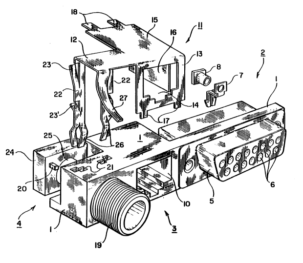
As shown in Figure 1, the connector of the first preferred
embodiment includes a combined housing 1 having a D-sub section 2, a
modular jack section 3, and a BNC section 4. The shared housing 1 is
5 preferably molded from a suitable plastic, in which case the housing can
easily be made in a variety of configurations for different connector
types, the illustrated types being typical of a network interface card.
The D-sub section 2 of the first preferred embodiment is
10 conventional in nature, except that its housing is integral with the
housing of the modular jack section. Included in this section are a
conventional metal shield 5 which surrounds a D-shaped front portion
including apertures 6 for receiving correspondingly shaped male or female
connector contacts (not shown). Unlike the standard D-sub connector,
15 however, the illustrated D-sub connector section 2 requires only a single
board lock 7 for securing the D-sub section on the board. An optional
connecting pin 9 for electrically connecting shield 5 with the board lock
to provide a ground path therethrough when the board lock is secured to
the circuit board may also be provided. Those skilled in the art will
20 recognize that the configuration of the rear portion of the connector
section, which is arranged to permit connections between the contacts
and the board, is conventional and may be varied according to the
specific requirements of the type of D-sub being implemented.
2~273
The modular jack section 3 of the connector has a shape
identical to the shape of the standard modular jack connector, except that
the housing is integrally molded with connector section 2 and 4. The
jack receiving aperture 10 in the front of the section, and all internal
5 components (not shown) are identical to those found in conventional jack
connectors. The principal departure from conventional connectors in this
section of the combination connector is that, instead of a conventional
stamped and formed shield case which fits over at least four sides of the
housing, a modified shield 11, which is also preferably stamped and
10 formed, is provided which is shaped to take into account the fact that
only three walls of the section are exposed, and which includes an
extension 12 for providing, as will be explained below, grounding in the
BNC section 4 of the combination connector.
The portion of shield 11 which covers exposed walls of the
modular jack section 3 includes a planar front portion 13 having a cutout
14 corresponding to the aperture 10 in the modular jack, a top portion 15
extending transversely to the front portion 13 which completely covers
the top of modular jack section 3, and a single side portion 16 extending
20 transversely to both the top and front portions of section 3, portion 16
being designed to fit between the D-sub connector section 2 and the
modular jack section 3. Also included in the illustrated embodiment are
pairs of tabs 17 and 18 which can be bent respectively over the bottom
and back of the modular jack section to secure the shield on the housing,
~17~/~73
although those skilled in the art will appreciate that numerous other
arrangements for securing the shield on the housing may also be utilized.
Shield 11 includes a lateral extension 12, as noted above,
5 which covers the top of the main body of BNC connector section 4 for
use as a ground connection in case the BNC connector is filtered. The
filtering arrangement and other aspects of the BNC section, including the
shape of a threaded front mating portion 19, are similar to those
disclosed in U.S. Patent Application 08/075,876, and includes filter
10 components, e.g., chip capacitors 20 inserted into slots (not shown)
which extend parallel to the direction of the BNC contact and which
communicate with vertical passages 21 formed in the connector housing.
Lateral extension 12 of shield 11 includes further extensions 22 which fit
into passages 21 and which include upper tines 23 and lower tines 23'
15 arranged to extend into corresponding ones of the chip capacitor slots
when extensions 13 are inserted into passages 21, thereby biasing any
chip capacitors present in the slots against a parallelepiped shaped rear
portion 24 of a metal BNC contact 25 of the type disclosed in the above-
mentioned application S.N. 08/075,876.
The shield 11 also advantageously includes an integral board
lock in the form of bifurcated portions 26 at the distal ends of extensions
22. Bifurcation of the ends of extensions results in the formation of
fingers which can bend inwardly upon passage through a hole in a circuit
~ 7~73
board and then outwardly when the hole is cleared to lock the connector
on the board in the manner of conventional board locks, but without the
need for an extra piece or assembly step. Also included in the shield is a
panel-engaging extension 27 similar to those described in copending
5 patent application Serial Number 08/075,876 for providing a ground path
from the shield 11 to a panel on the circuit card or device to which the
connector is mounted.
Referring now to Figures 2-4, a combination connector
10 according to a second preferred embodiment of the invention includes a
modular jack section 103 having a shape identical to the shape of a
standard modular jack connector, except that the housing is integrally
molded with BNC connector section 104. Except as noted below, all
components of both the modular jack section and the BNC section are
15 standard, and thus only those features which represent improvements
over conventional connectors of the subject types, or which are
necessary for an understanding of the invention, are illustrated.
The body of the modular jack portion 103 of the combination
20 connector illustrated in Figures 2 and 3 is identical to the modular jack
disclosed in copending U.S. Patent Application S.N. 08/043,544, and
includes a jack receiving aperture 105, openings 106 at the top of
aperture 105, and grooves 107 in the top surface of the jack section for
receiving contacts 98 and 99 having a generally standard configuration.
~1 7~2~3
Extending into the top surface of the jack section 103, towards the rear,
are openings 108 into which may be placed filter elements (also not
shown) .
As explained in the copending application, the contacts are
positioned such that, when filter elements are place in the openings,
electrodes on the filter elements engage the contacts.
As in the previous embodiment, the combination connector
10 of this embodiment includes a single stamped and formed shield member
109 which includes a front wall 110 having a cutout or openiny 111
corresponding in shape to the shape of the jack-receiving aperture 105, a
top 1 12, a side wall 1 13, and an extension 1 14 of the top which covers
the top surface of the BNC section 104 of the combination connector.
15 Also part of the single shield member 109 are side walls 1 15 and 1 16 for
respectively shielding remaining exposed sides of the modular jack and
BNC sections of the connector. In addition, the shield member may
include extensions (not shown) at the rear of the respective connector
sections. As is apparent in Figure 2, front wall 110, top portions
20 1 12,1 14, and side walls 1 13, 1 15, and 1 1 6 are all mutually
perpendicular.
The top of the shield member also includes, in the illuslrated
embodiment, downwardly extending tines 117 for engaging, in the
21 7`~273
manner disclosed in copending application S.N. 08/043,544, ground
electrodes on any filter elements which have been inserted into openings
108. The shield member may be secured to the housing by tabs 1 18
which can be bent at a ninety degree angle to engage the bottom of the
5 connector once the shield has been positioned on the housing, although
those skilled in the art will appreciate that numerous alternative means
may be sued to secure the shield on the connector.
The BNC section 104 of the combination connector includes
10 two unique features which may also be used in stand-alone BNC
connectors:
The first of these particularly unique and advantageous
features is that all insulating portions of the BNC section, including the
15 conventionally separate insulators 161 and 162, respectively, which
surround the inner and outer coaxial contact, are molded in a single mold.
Thus, the entire connector, including both the jack and BNC portions
may be produced in a single step, without even the need for separate
molding and assembly of the inner insulator.
This feature is accomplished, as is best shown in Figure 3,
by forming a single front insulating portion 1 19 of BNC section 103 with
an annular groove 120 for accommodating the outer contact 121 and
which separates insulators 140 and 141, and a cylindrical bore 122 in the
~17427~
portion of the insulator which lies within the groove 120 for
accommodating the inner contact 123, and providing at the rear of the
groove 120 which accommodates the outer contact 121 a through-hole
124. The outer contact 121 can thus be connected to the circuit board
5 (not shown) on which the combination connector is mounted by providing
an extension or a discrete contact pin 125 secured in bore 126 in the
outer contact, and which is inserted through through-hole 124 as outer
contact 121 is positioned from the front of the connector during
assembly in the annular groove. After insertion, pin 125 is normally bent
10 so that it extends downward past the rear of the BNC section to engage
the circuit board, although those skilled in the art will appreciate that the
principles of the invention will also apply to a vertical, as opposed to right
angle, connector configuration (particularly in the case of a stand-alone
BNC connector), in which case pin 125 would not be bent. As is
15 conventional, the inner contact also includes an extension which is bent
downward after insertion of the inner contact to engage an appropriate
lead on the circuit board.
Filter capabilities are provided, according to a second unique
20 and particularly advantageous feature of this embodiment, by an
especially simple structure involving the inclusion of flanges 130 on the
outer contact 121, as shown in Figures 2 and 4. Flanges 130 have an
upwardly facing planar surface 131 for contacting the live electrode 132
of a chip capacitor or other filter element 133 placed into openings 136.
~I 74 2 7~
The ground connection provided by the filter elements can then be
completed simply by causing downwardly extending tines 134 cut out of
the shield member 109 to engage a ground electrode 135 on the filter
element, the tine biasing the filter element against the planar surface of
5 outer contact 1 21 contact.
Also included as part of shield member 109 of this
embodiment is a panel-engaging tongue 137 for directly grounding the
shield member to a panel provided on the interface card, in the manner
10 disclosed in copending application S.N. 08/075,876. Finally, while a
separate board lock 138 is illustrated for this embodiment, it would of
course also be possible to modify the shield casing to include a board lock
in the manner similar to that of the first embodiment.
Those skilled in the art will appreciate that while filtering is
required for some applications, the filter components may be omitted in
others. Nevertheless, because the inclusion of component slots during
the housing molding process requires no extra steps, and because
mounting of the shield on the connector requires the same number of
20 steps regardless of whether the filter components are included, the same
housing and shield structure may be used for either the filtered or
unfiltered situation, and the scope of the invention is intended to
encompass both situations.
217427~
Referring now to Figures 5 and 6, the connector of the third
preferred embodiment of the invention includes single molded housing
201 made up of a BNC section 202 and a modular jack section 203.
Except as noted below, all components of both the modular jack section
5 and the BNC section are standard, and thus only those features which
represent improvements over conventional connectors of the subject
types, or which are necessary for an understanding of the invention, are
illustrated.
The BNC section 202 of this embodiment may be identical to
the BNC sections illustrated in any of Figures 1-4, including outer contact
204, outer insulator 205, inner contact 206, inner insulator 207, and
board locks 208, although the particular configuration of the BNC
connector can also be varied in ways not described above so long as the
15 BNC section fits within a desired BNC connector profile. For example, as
illustrated, the conductive path to the outer contact is provided by
resilient contact finger 210 extending from contact 211.
The modular jack section 203 of the embodiment illustrated
20 in Figures 3 and 4 can also be identical to corresponding modular jack
sections of the embodiments illustrated in Figures 1-3, except for the
presence of LED receiving openings 209, and can also be varied in ways
not described above while still fitting within a modular jack profile.
Included in the modular jack section of this embodiment are a boardlock
18
21 7427~3
214, a jack receiving aperture 215, and grooves 217 in the top surface of
the jack section for receiving contacts 218 having a generally standard
configuration. Although the shielding 219 in this embodiment is
illustrated as only covering the BNC section of the combination
5 connector, it will be appreciated by those skilled in the art that the shield
may be extended in the manner as illustrated above, including appropriate
tabs for engaging filter components in either or both sections of the
connector. It will be noted by those skilled in the art that if a combined
shield is used, the shield would need to be modified to provide openings
10 for the LED elements in the modular jack section.
The LEDs 212 are accommodated in this embodiment of the
invention by providing the openings 209 within the stepped portion of the
standard modular jack interior profile, into which are inserted LEDs 212
15 from which extend contacts 222 and 223. To accommodate contacts
222 and 223, openings 209 are continued by grooves 224 which extend
rearwardly from openings 209, the contacts being bent at a ninety degree
angle to exit the grooves and engage appropriately positioned terminals
on the circuit board. This arrangement of the LEDs simplifies insertion
20 and removal of the LEDs in comparison with the LED arrangement
disclosed in U.S. Patent Number 4,978,317, in which the LED contacts
are molded into the top and rear of an RJ connector. It will be
appreciated, however, that the specific manner in which the LED contacts
of the present invention are arranged may be varied by those skilled in
19
~17~73
the art, as may the location of the LED in the combination connector, and
even the nature of the indicator, which may also be in the form of optical
waveguides, incandescent lights, and other fighting arrangements
sufficiently small to be mounted in the housing of a combination
5 connector.
A particularly advantageous feature of this embodiment of
the invention, which could be used in connectors other than a
combination connector, is that the openings are exposed at the lower
10 surface of the connector which mounted on the circuit board, the LEDs
being held in place by shoulders 225 at the lower parts of the openings.
Placement of the LEDs adjacent the lower surface of the connector has
the advantage of minimizing the required contact length and exposure of
the openings to the lower surface facilitates insertion and removal of the
15 LEDs. Such insertion and removal is not possible in a molded-in
arrangement of the type disclosed in U.S. Patent No. 4,978,317.
It should be apparent from the above description that the
connectors of the preferred embodiments contain an absolute minimum of
20 parts. A list of parts which must be assembled for the two embodiments
is as follows:
1. a plastic housing for both the RJ 45 jack and the BNC
connector, which may include both the inner and outer BNC insulators
(those skilled in the art will appreciate that the one piece insulator design
~ 7~2~3
used in the second embodiment may also be adapted for the first
embodiment~,
2. a shield casing common to both connectors which
also facilitates filtering, and
3. optionally, an LED and contacts therefor.
The only remaining elements necess~ry to complete
functional connectors are the modular jack and BNC contacts. To add
filtering, the assembler merely needs to insert capacitor chip or other
10 appropriately sized filter chips into openings provided in the modular jack
and BNC sections of the respective preferred connectors. No extra parts
are requlred.
In order to assemble the preferred connectors, the modular
15 jack, BNC, and, if applicable, multiple pin parallels connector contacts
need to be inserted into the respective connector sections, followed by
insertion of any desired filter chips, and placement of the combined shield
casing over the plastic insulative one-piece molded housing. Thus just
two basic assembly steps (three if filtering is desired, are necessary to
20 complete assembly of a fully functional combination connector.
Because the modular jack shield and BNC ground connection
are stamped from a single sheet of conductive metal, and because of the
shared walls, less metal is required and at the same time a single
~7~273
assembly step suffices to provide both the necessary shielding for both
the modular jack and the grounding for the BNC connector. Those skilled
in the art will, however, appreciate that numerous variations in the
concept of a common shield can be provided, including designs which
5 merely I O provide a shielding function rather than a filtering function,
and designs for various types of connectors other than the three types of
connectors shown. As a result of such possible modifications, and others
which will undoubtedly occur to those skilled in the art, it is intended that
the invention not be limited by the above description or the attached
10 illustration, but rather that it should be limited solely in accordance with
the appended claims.