Note: Descriptions are shown in the official language in which they were submitted.
21 74~û4
960001-shf
GR 95P5515 US
IN THE UNITED STATES PATENT AND TRADEMARK OFFICE
"CIRCUIT FOR PULSED OPERATION OF A DISCHARGE LAMP"
Reference to related patents and applications assigned to the
assignee of the present invention, th~ ~ioclo~ur~s of which a
~.x~hy ineol~LdL~d by re~L~r.c: ~ '
U.S. Patent 4,792,887, Bernitz et al.
(Attorney Docket 87363-shf; 15 397 US);
U.S. Patent 5,198,728, Bernitz et al.
(Attorney Docket 910810-shf; GR 91P5501 US);
U.S. Patent 5,396,152, Boenigk
(Attorney Docket 930022-shf; GR 90P8100P US);
U.S. Patent 5,481,162, Boenigk et al.
(Attorney Docket 930715-shf; GR 93P5503 US);
U.S. Patent 5,483,126, Boenigk et al.
(Attorney Docket 930714-shf; GR 93P5502 US);
U.S. Application S/N 08/539,882, filed Oct. 6, 1995, Bernitz et al.
(Attorney Docket 950370-shf; GR 94P5544 US);
U.S. Application S/N , filed , Osterried et al.
(claiming priority German Appln. 195 07 553.6, March 3, 1995;
Attorney Docket 950605-shf; GR 95P5506 US);
U.S. Application S/N , filed , Osterried et al.
(claiming priority German Appln. 195 09 832.3, March 17, 1995;
Attorney Docket 950677-shf; GR 95P5509 US);
U.S. Application S/N , filed , Huber et al.
(claiming priority German Appln. 195 15 511.4, Apr. 27, 1995;
Attorney Docket 950768-shf; GR 95P5516 US);
Reference to related publication assigned to the assignee of the
present invention:
European 0 485 865 A1, Bernitz et al.
2 1 746Q~
-
FIELD OF THE INVENTION.
The present invention relates to a circuit to operate a
discharge lamp, and especially a high-pressure discharge lamp
with energy supplied in pulses, and to an electronic accessory or
ballast unit which includes the circuit.
BACKGROUND.
Discharge lamps and especially high-pressure discharge lamps
are customarily operated by pulocd currents in which, usually,
the amplitude of the lamp current is maintained to be essentially
constant over time. The shape of the waveform or of the curve of
the current, based on the technical characteristics of the
accessory or ballast circuit, may vary, for example, the ballast
may provide a sine shaped, triangular shaped, or rectangular
shaped lamp current pulse.
It has been found that d-ffcrcnt types of discharge lamps
may provide light having different parameters when the energy
supplied to the lamps is in the form of short sequential pulses
or pulse groups. The average energy supplied, in spite of the
pulsed supply, ~ not exceed the lamp power which is determined
by the structure of the lamp itself, in order to obtain changes
in the light technological parameters. For example, sodium high-
pressure discharge lamps can be controlled to operate to provide
a light spectrum having a color temperature of about 3,000 K, and
more, by changing the electrical operating characteristics of the
energy supply.
In pulsed operation, high energy is supplied to the lamp for
a short period of time, with a predetermined repetition frequency
fw, of for example between about 150-400 Hz. This pulse energy
may be above the average lamp power by a factor of more than 20.
This high energy phase, which will occur in a second operating
state (to be defined and discussed below) can be formed by a
single pulse, or by a sequence of pulses or oscillations, in the
form of pulse groups, or in the form of a burst. This high-
~ , ~3 ~ 2 ~ ~ ) ~.3.~l~
. ~ .. . .. . , . . . ... , . . . . ~ ...... . . .. . .. ... . . .. .
21 74604
.
energy supply phase is also often referred to as a c~mpling orpower campling phase since, to generate this pulse burst, the
operating mode of the accessory or ballast circuit must be
switched over from another operating mode. The duration of this
power phase, typically, is only a fraction of a period of the
repetition frequency, for example 1/20 Tw, in which Tw is the
duration of a period of the repetition frequency. A holding
phase, which can also be termed a "first operating state" is
placed between the power bursts or power phase, in which only so
much power is fed to the lamp that the discharge can persist
until the next power pulse occurs. Otherwise, a new ignition
would be required for each power phase.
The referenced U.S. Patent 5,396,152, Bonigk, the disclosure
of which is hereby incorporated by reference, describes a circuit
arrangement for pulsed operation of a high-pressure discharge
lamp. The discharge lamp is connected to a d-c source thro h a
Co~pFisi~g two power switching elements formed, for example, by a ~gamp choke,
halr-~rldge circuit/. An inductive reactance/is connected in
series with the lamp formcd, for cxamplc, by a lamp choke. A
further inductive reactance can be connected in parallel to the
lamp choke to change the energy storage capacity of the circuit.
The additionally connectible inductive reactance permits
operating the lamp with different electrical parameters in the
power phase, or in the holding phase of the lamp, respectively.
The circuit requires an additional power switching element
besides the power switching elements included already in the
half-bridge, in order to permit selectively connecting the
additional inductive reactance. This additional power switch
causes a relatively large energy loss due to the voltage drop
thereacross and the pulse current passing therethrough.
Additionally, such a power switch is expensive; if the power
switch is in the form of a semiconductor, it must be designed to
have a blocking voltage of over 400 V, while being capable of
carrying currents of 30 A, or more. The additional reactive
2 1 74604
impedance further requires an additional circuit element, which
must be wired and connected. The main reactive impedance, as
well as the additional reactive impedance within the circuit loop
including the lamp, must also be constructed to be capable of
accepting high voltages which arise during ignition of the lamp,
namely the lamp firing or ignition pulses.
THE INVENTION.
It is an object to provide a circuit for pulsed operation of
discharge lamps, and an electronic accessory or ballast unit
including such a circuit, in which the number of circuit
components can be further reduced.
Briefly, the reactive impedance in circuit with the lamp is
so constructed that it has a reactance value characteristic which
is non-linear, and particularly which is non-linear with respect
to current flow therethrough.
The circuit for pulsed operation of the discharge lamp, and
particularly of a high-pressure discharge lamp contains, as
known, at least a half-bridge with two switching elements, for
example transistors. The half-bridge generates an essentially
square-wave alternating current at the center of the bridge, that
is, at the junction between its two switching elements. A
reactive impedance is connected in series with the lamp. The
lamp is further coupled to an ignition circuit. In accordance
with the present invention, the reactive impedance is a non-
linear reactance.
The circuit and the ballast unit, in contrast to the priorart, require only two power switches, typically semiconductor
power switches, and only a single reactive impedance element in
the lamp circuit. Switch-over between two operating states or
phases, for example the first operating or holding phase and the
second operating or power phase, is automatically obtained by the
reactive impedance which has the non-linear reactance.
Preferably, the reactance can be switched essentially between two
21 746(~4
values. By suitable dimensioning, the best suitable operating
currents can be obtained for the respective operating phases of
the lamp, that is, the power phase and the holding phase. The
relationship of the two reactance values is preferably between 10
and 50; a particularly preferred relationship is about 40.
The reactive impedance in the lamp circuit, typically the
lamp choke, is, in accordance with a specifically preferred
embodiment, formed as a non-linear inductance.
The non-linearity of the inductance can be obtained,
preferably, by providing a ferrite core for the coil which has a
center leg which, at least in part, is decreased in size with
respect to outer legs. The non-linear reactance may also be
formed by providing two torroidal or ring cores of different
material characteristics. Preferably, one of the ring cores is
made of a low permeability powdered material with high saturation
magnetization; the other ring core is made in the form of a high
permeability ferrite core with low saturation magnetization.
Both ring cores are mounted one above the other.
The accessory unit has the circuit previously described. A
control circuit is provided to control the operation of the
switching elements in the circuit.
Preferably, the operating current in the first operating
state is between about 0.3 and 0.5 A, at a frequency between
about 80 kHz and 100 kHz. In a second operating state, the
current is preferably between about 20 A and 30 A, and the
frequency between 15 kHz and 25 kHZ. A particularly suitable and
hence preferred frequency is 80 kHz in the first operating state
and 20 kHz in the second operating state. In accordance with a
preferred example, the temporal relationship of the first
operating state to the second operating state is between about 10
and 30; the duration of the second operating state, that is, the
power phase, may, for example, be about 200 microseconds, at a
repetition frequency of, for example, 200 Hz.
--5--
21 74604
-
In accordance with a particularly preferred embodiment of
the electr ~ accessory~unit, the power circuit arrangement and
the control circuit are coupled inductively. Preferably, a
control transformer is provided having a primary winding and two
secondary windings. The switching elements are, preferably,
power semiconductors, especially insulated gate bipolar
transistors (IGBT). Such power transistors can be easily
controlled and have low switching losses, while carrying high
currents.
Ignition of the lamp, preferably, is obtained by an ignition
system which can be formed by at least one additional winding on
the non-linear reactive impedance. Thus, the non-linear reactive
impedance, preferably a non-linear inductance, obtains a further
function, namely to generate and transmit the ignition pulse.
The discharge lamp can also be fired or ignited by means of
a capacitative element connected in parallel to the discharge
lamp. This capacitative element, typically a capacitor, together
with the non-linear reactance, forms a series oscillatory or
tuned circuit. If the ignition pulse is generated by the
additional capacitor-reactance circuit, the additional winding on
the non-linear inductance, as well as the switching components to
generate a voltage pulse on the additional winding can be
omitted.
Various types of d-c current supply circuits use an
intermediate circuit capacitor at the output of the d-c source,
typically a rectifier. In accordance with a feature of the
invention, the intermediate capacitor is replaced by two serially
connected capacitors, and the junction of the serially connected
capacitors is connected to the discharge lamp. The coupling
capacitor thus can be eliminated, thereby reducing the volume of
the overall accessory circuit substantially. The arrangement has
the additional advantage that the serially connected capacitorS
can be provided in the form of ~ electrolytic capacitorswhich,
Y6
.
21 74604
in the pulse operation and in contrast to a coupling capacitor
which customarily was a foil wound capacitor, will be noiseless.
DRAWINGS.
Fig. 1 is a highly schematic block diagram of a circuit in
accordance with the present invention, and having an additional
ignition circuit;
Fig. 2 illustrates another embodiment of the present
invention with a resonance ignition circuit;
Fig. 3a illustrates a ferrite core having a center leg of
reduced size to form a non-linear inductance;
Fig. 3b is a top view of the core Fig. 3a;
Fig. 4 is a pictorial view, sectionalized, through a ring
core made of two different materials to form a non-linear
inductance; and
Fig. 5 is a graph which illustrates the dependence of
inductance of the non-linear reactance (ordinate) as a function
of lamp operating current (abscissa).
2? 14f~Q/4
DETAILED DESCRIPTION.
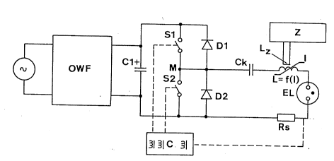
Fig. 1 illustrates the basic circuit which includes a
circuit arrangement OWF comprising a rectifier adapted for
connection to an a-c power network, and including an active
harmonic filter for power factor correction. The power source
may, for example, be a 220 V power network. The output of
circuit OWF provides an essentially constant d-c voltage of about
400 V.
An intermediate capacitor C1 is connected to the output
terminals of the harmonic filter OWF for buffering the output
energy while the a-c power wave goes through zero or null. The
circuit according to the present invention is connected to the
output terminals of the filter as well, to operate the discharge
lamp EL. Preferably, and typically, the discharge lamp EL is a
high-pressure discharge lamp.
The essential elements of the circuit in accordance with the
present invention are two power switches S1, S2, arranged in
half-bridge configuration and having a common junction M,
generating a square-wave alternating voltage. The switches Sl,
S2 are controlled in push-pull from a control unit C. Typically,
the switches S1, S2 are semiconductor switches.
An inductive reactance formed by a lamp choke ~ is
connected in series with the lamp. A coupling capacitor Ck forms
an additional energy storage element in the loop circuit which
includes the lamp. Two diodes D1, D2 are connected in parallel
to the switches S1, S2 to provide free-wheeling or by-pass to the
switch units. The diodes D1, D2 are polarized in blocking
direction with respect to the direct voltage of the rcctificr and
harmonic filter OWF.
The lamp is started or fired by an ignition circuit Z, and
applying ignition pulses by an additional winding on the
inductive reactance L. The ignition circuit Z provides a voltage
pulse which is coupled by the additional winding Lz, shown only
-8- ~ ~
21 74604
schematically. The ratio of turns of the auxiliary winding and
of the winding of the inductive reactance is so selected that a
high voltage pulse is generated at the side of the reactance
adjacent the lamp, in order to fire the discharge lamp.
A current measuring resistor Rs is connected in series with
the discharge lamp L. The resistor Rs may be a portion of the
control circuit C or, respectively, can be connected directly
therewith. The control circuit C controls the operation of the
switches S1 and S2. At the common junction M, a square-wave
voltage of predetermined frequency is generated. The switches S1
and S2, in the first operating state, are operated at a
relatively high frequency F8, and in a second operating state
with a relatively low frequency FT.
Details of the basic circuit described above are described
in the referenced U.S. Patent 5,396,152, Bonigk, the disclosure
of which is hereby incorporated by reference.
In accordance with a feature of the present invention, the
reactive impedance formed by the choke L has a reactance which
is non-linear, and which depends on the current flowing
therethrough. The operating current of the lamp, derived from
the switches Sl and S2, is determined by the reactive impedance
of the non-linear reactance L and, of course, the square-wave
voltage applied thereto. In the first operating state,f in which
the switches operate at the relatively high frequency ~ the
3trong current I8 to operate the discharge lamp EL Wi11 have
values in which the non-linear reactance L at the most has a
first value of L'; during the second operating state, with a
relatively lower frequency ~, the current IT to operate the
discharge lamp EL will have values in which the non-linear
reactance L has a reactive impedance which is between a first
value L ' and a second value L " .
The current measuring resistor Rs is used to control current
amplitude by varying the switching condition, and hence the
I ~,3.~ ~ ~ ~ 3 ~6
2 1 74604
_
impedance value of the non-linear reactance L which, for
example, can be controlled by the influence of temperature f a
core material within the core of the reactive impedance L. The
operation of the non-linear inductive reactance will be described
below with reference to Fig. 5.
Fig. 2 illustrates another embodiment of the invention. The
difference with respect to the embodiment described in Fig. 1 is
the arrangement for firing the lamp, and the filtering of the
output from the rectifier-harmonic filter OWF.
The ignition circuit Z (Fig. 1) need not be used. Rather, a
resonance capacitor CR is connected in parallel to the lamp EL,
to provideJ in combination with the non-linear reactance L, a~
respn~nce flring
~gnltlon pul~c for the lamp. The intermediate capacitor C1
which, in Fig. 1 is connected to the output terminals of the
filter OWF, is, rather, separated into two capacitors C2, C3,
which define a common junction J. Together, they have the same
effect as the capacitor C1 of Fig. 1. Preferably, the value of
capacity of the capacitors C2, C3, serially connected, is ~out
the same as the capacity value of the capacitor C1. This
arrangement permits elimination of the coupling capacitor Ck, and
the lamp EL is then connected to the common junction J between
the capacitors C2, C3 and through the non-linear inductance L
to the common junction M between the switches S1, S2.
The circuit according to Fig. 2 replaces the pulse ignition
from the circuit Z (Fig. 1) by resonant voltage enhancement of
the resonance circuit by the capacitor CR and the inductance L.
The advantage of the pulse ignition according to Fig. 1 is a low
power use to build up the high voltage, and excellent
reproducibility of the ignition voltage over the lifetime of the
accessory circuit. The advantage of the circuit of the second
embodiment is that it permits the use of two separate
intermediate circuit capacitors which can be formed as
electrolytic capacitors, eliminating the coupling capacitor Ck.
--10--
l ~ 21 746Q4
_
The coupling capacitor Ck, typically, is a wound foil capacitor
which, in the course of time, may become noisy. Furthcl,..o~ c
oxtra winding T~ on thc inductancc L can bc omittcd. The
control circuit C preferably includes inductive coupling to the
switches S1, S2, as schematically shown in Fig. 1. The control
circuit C, and the current measuring resistor Rs has been omitted
from Fig. 2 for clarity of the Figure; it can be connected
similarly as shown in Fig. 1.
Operation, with reference to Fig. 5:
Fig. 5 illustrates the course of inductance of the non-
linear impedance L with respect to lamp operating current IL
The basis for dimensioning and the construction of the non-linear
reactance is formed by the first and second operating states (not
and (not shown in Fig. 5)
sho~m in Fig. ') at the respective frequencies fH and f~/. The
operating currents, as well as their time duration and the
relative time durations, provide the desired light parameters of
the lamp.
In a first operating state, namely a holding state or
holding phase, the operating current IL has a small value,
indicated at IH~ SO that the inductance will have a relatively
high impedance and a high inductance value L'. In this state,
the inductance is not saturated. In the second operating state,
that is, during the power phase, the operating current IL is
high, as shown by the current value IT SO that the impedance, and
hence the inductance L", is relatively low. Under this
condition, the inductance is saturated. Switch-over between the
two operating phases is obtained by change in frequency in
control of the two power switches S1, S2 (Figs. 1 and 2). Fig. 5
shows ideal switching conditions in the respective operating
phases in solid line i~/and the actual course/of the function L,
which is a function of current or, mathematically,
L = f(I).
The reactance value L, hence can be switched between the two
3 ~6
2 1 74~04
values L' and L" . The ratio L' /L" should be between about 10 and
50, and preferably is about 40.
The switch-over point or, respectively, the transition
region will depend on the temperature of the core material (Figs.
3 and 4) of the non-linear reactance L .
The switch-over region between L', that is, wit~ an 1 t d
unsaturated inductance, and L", with a saturated inductance,/that
at the maximum arising operating current in the first operating
phase, namely the holding phase, and the maximum arising core
temperature, the core will not reach the saturation value. In
accordance with a feature of the present invention, disturbing
temperature influences can be compensated for by suitable control
of the lamp currents by measuring the lamp currents by the
measuring resistor Rs, and providing a control value to the
control circuit C. Thus, disturbing temperature influences on
the reactance L, which is a cored reactance, can be eliminated.
The second operating state, when IT flows through the
saturated reactance L", is shorter than the first operating
state, when current IH flows through the unsaturated reactance
L'. The temporal duration between the first operating state or
phase and the second operating state or phase is between about 10
and 30.
The inductance values, as a function of current, can be
obtained by using a customary, commercial construction of a
ferrite core, having the usual commercial designations E, RM, P,
ETD, and the like. The center leg of the core, as best seen in
Figs. 3a and 3b, is made smaller than the outer legs thereof.
This shape can be obtained by taking a standard core and grinding
it to the desired shape; alternatively, specially pressed or
compacted cores with the special shape predetermined can be used.
The center leg can be decreased in cross-section over its entire
length or only over a portion thereof. Fig. 3a and Fig. 3b show
one example of a core which has a center leg partially
8~ 3~ Y6
2i 74604
constricted with respect to the outer legs.
Another way to obtain a reactance in which the inductive
reactivity changes with current is to combine two ring cores of
different material characteristics. A low permeability powdered
core A formed, for example, of iron powder, permaloy powder or
the like, with high saturation magnetization, is secured on a
high permeability ferrite core B of low saturation
magnetization. The two cores can be connected together, for
example, by an adhesive. Both cores are then wound conjointly.
Fig. 4 illustrates a half-section through such a core.
The circuit in accordance with the present invention is
preferably operated by providing for the first operating phase,
that is, the holding phase, a holding current of 0.3 A to 0.5 A,
and at a frequency of between about 80 kHz to 100 kHz. A pulse
current of from 20 A to 30 A at a frequency of 15 kHz to 25 kHz
is provided during the power phase, that is, the second operating
state or phase. The second state, during which the power burst
is supplied, is short and has a duration of typically about 200 ~s.
This means that a burst or package of pulses during the power phase
will have about six individual oscillations or periods. The
repetition frequency of these bursts or, respectively, of the power
phase, may vary between about 160 Hz and 400 Hz.
The switches Sl and S2 preferably are power transistors and are
controlled in push-pull, inversely with respect to each other, with a
duty cycle of about 50~. Preferably, insulated gate bipolar
transistors (IGBT) are used. The IGBTs are inductively controlled by
a control transformer, integrated in the control circuit C, and shown
only schematically in Fig. 1. Such a control transformer may have a
primary winding of about 50 turns and two separate secondary windings
of, each, 120 turns.
In accordance with a feature of the invention, the power portion
of the electronic accessory circuit for pulsed operation of a
discharge lamp requires only two power switches S1, S2. Switch-over
-13-
-
21 74~0~
between the operating phases of the lamp, namely the holding phase and
the power phase, is obtained by the non-linear reactance in series
with the lamp and in the lamp circuit. The reactive impedance of this
reactance element L is dependent on current flowing therethrough.
The operation of the lamp in the holding phase or in the power phase,
respectively, requires currents of highly different current values
cause
which can bc obtaincd ~ithout cxtcrnal switchc~ by fo.",in~ th~
reactanceS L with relatively different reactance values in the
holding.phase and in the power phase, respectively.
Various changes and modifications may be made, and any features
described herein with respect to one embodiment may be used with any
of the other embodiments, within the scope of the inventive concept.
"~.3 ~G ~ ~
-14-