Note: Descriptions are shown in the official language in which they were submitted.
WO 95/13567 Z -I '1 4 PC''/iJS94/11913
1
PROCESS FOR MAKING AN ARRAY OF
TAPERED PHOTOPOLYMERIZED A GUI ES
P , File 82 3307 (6100)
Background of the Invention
The present invention relates to a process for making an array of
tapered photopol erized waveguides.
VJave des, also known in the art as li t transmissive devices
or light des, are used in display devices, such as for example
projection display devices, off screen display devices, and direct view
displays. See for example U.S.1'atents 3,218,924 and 3,279,314 to
Miller and U.S. Patent 4,767,186 to Bradley, Jr. et al. Such displays
are used in a wide range of applications inclu ' g computer terminals,
airplane cockpit displays, automotive ent panels, televisions,
and other devices that provide text, grap 'cs, or video ' o ation.
Processes for making waveguides for use in display devices are
lano .For example, U.S. Patents 3,218,924; 3,279,314; and
2 o 4,767,186 teach that projection screens may be manufactured by
known processes and list compression molding, injection ffiol ' g,
extrusion, hot roller pressing, cas ' g, and photopol e' tion. U.S.
Patent 3,767,445 teaches a method for producing inte ted optical
waveguides by making a die ha ' g a surface ffiatc g the desired
2 5 oran cross section waveguide shape, embossing a transparent
plastic substrate with the die, and coa ' g the embossed substrate with
a high refractive index material.
U.S. Patent 5,230,990 teaches a process for making optical
waveguide array of li t trmsmissive cores with uniform cross section
30 throughout the core length. A resist master is formed first by exposing
a photoresist layer through a photomask, ssol ' g the exposed areas,
and heating the non exposed areas to form p el rows of semicircular
shaped protuberances. The resist is heated until it is mehed and the
liquid surface tension draws it into a line of a semicircular cross section
35 or a hemispherical bead. Thus, semicircular grooves and henn.ispherical
dots are the only shapes a able with this method. A stamper is then
formed from the resist master by sputte ' g electroconductive film
li
CA 02174851 2004-05-03
o il
2
on the resist master to form a metal master and then forming a metallic
film on the metal master to form a stamper having parallel rows of
semicircular shaped protuberances. The stamper is then used to form
the optical waveguide array by exposing a low refractive index material
on the stamper, removing the -cured layer, putting a high refractive
index material into the semicircular shaped grooves of the cured layer,
curing the high refractive index, putting a low refractive material on the
high refractive index material, and curing. See also U.S. Patents
4,902,086; 5,113,471; and 5,136,678.
ia Kokai Patent Publication 245106 published October 31, 1991
teaches a process of making an optical plate of a substrate having high
refractive index waveguides with uniform cross section throughout the
waveguide length, wherein the waveguides are separated by low
refractive index material. The optical plate is made by placing high
i.s refractive index photosensitive resin on a substrate, covering the
photosensitive resin with a low oxygen permeable sheet, and exposing
the photosensitive resin to ultraviolet light through a photomask and the
low oxygen permeable sheet to form uniform cross section waveguides.
The unexposed resin and low oxygen permeable sheet are removed and
20 low refractive index material is placed around the waveguides.
The 245106 process is disadvantageous because it produces
waveguides which when used on a display, would suffer from low
contrast and changes in visual chromaticity as the viewing angle
changes. In order to obtain good collection of light at the input end of
25 the waveguides, they must be close packed at the input end, as taught
in Kokai 245106. Since the cross-section is uniform, this close packed
arrangement persists throughout the optical plate, along the length of
the waveguides. This results in difficulty in removing the unexposed
material from the wall area during the development step and
30 additionally, does not provide space on the output end of the plate for
contrast improving materials to be added. Moreover, waveguides with
uniform cross section do not increase the angular distribution of the
light which passes through them. It is often highly desirable that the
waveguides should cause such an increase in angular distribution as is
35 taught in U.S. Patent Number 5,481,385.
WO 95/13567 21PCT/US94/11913
~~~
3
Other processes for making optical waveguides having uniform
cross section are disclosed in U.S. Patents 4,783,136 and 5,138,687;
European Patent Publication 357396 published March 7, 1990; Kokai
Patent Publication 24121 published February 2, 1993; and Kokai
Patent Publication 119203 published May 18, 1993.
U.S. Patent 4,712,854 teaches two processes for fo ' g optical
waveguides suitable for connection to optical fibers. The first process
involves a first ultraviolet light exposure step to form a refractive index
profile in the depthwise direction of the photopolymerization material
lo and a second ultraviolet light exposure step te form a refractive index
profile in the widthwise direction to form optical waveguide having
good ffiatc ' g characteristics relative to a graded index type optical
fiber. This process is disadvantageous because two ul violet light
exposure steps are required. In addition, no relief age is formed and
the waveguide consists of a higher refractive index region widiin a
sheet of continuous polymer film, or a lamination of several of such
fihns. Optical waveguide propagation is therefore strictly limited to the
plane of the film, never to propagation normal to the film surface.
Kokai Patent Publication 42241 published September 19, 1986
teaches a process of making a lightguide array by moving a substrate
through a container of monomer solution w e exposing the solution to
ultraviolet light through a photomask so that uniform cross section
li t de bodies form on the substrate. During the process, the
monomer solution being exposed is positioned between the photomask
and substrate and the photomask is positioned between the ultraviolet
li t and the monomer solution. During the exposure, the substrate is
moved pe en 'cularly away from the li t source. The substrate is
then removed from the container and a lower refractive index ffiaterial
is poured around the rod-shaped li t de bodies and cured. Tapered
light de bodies are formed by positio g a lens between the
photomask and monomer solution and ffio g the lens, thereby altering
the mask image magnification, so that the li t de bodies taper in a
direction away from the substrate toward the lens, photomask, and
ultraviolet light. The complicated rno ' g mask and lens system makes
this process disadvantageous to use. Also, this process is incapable of
making tapered light de bodies wherein the center-t enter distance
WO 95/13567 2_ 117 A 8 PC'1Yi7594/11913
4
between light input surfaces of adjacent bodies is substantially equal to
the center-to center distance between light output surfaces thereof
As a result, the area of the input and output surfaces of the array cannot
be equal. The array area at the tapered end is decreased by the square
s of the reduction ratio of the u*adividual elements, as is clear from the
diagr s of Kokai 42241. This method is therefore of no use for
creatmg tapered waveguide arrays for use in display applications such
as liquid crystal displays (I.CD's), as it is hi y undesirable to shrink
the size of the display. Further, the cross sections of individual
io elements i~ array created by a rno ' g lens are not uniform.
which are close to the optical axis of the lens system have a different
cross-sectional profile than those lying at the pe ' eter of the array.
This effect is so clearly shown in the diagrams of Kokai 42241. As a
result, the individual elements of the array wiU have non optical
15 properties, which is highly undesirable in display systems where such
non o ties would degrade the image qualities.
such, the need exists in the art for a s' ple process for
making array of tapered photopol e ed waveguides wherein the
array of tapered photopol e' ed waveguides has improved
20 properties.
Su a of the Invention
We have developed a process for making array of tapered
photopol e' ed waveguides which responds to the foregoing need irl
25 the step (a), a photomask is placed in substantial contact with a
subs te wherein the photomask has opaque and ft-ansparent r ons.
step (b), a subs ti y uniform thickness of photopol e' ble
mixture is placed on the subs te so that the subs te is positioned
between the photopol e' ble mixture and the photomask wherei~
30 (i) the photopol e' ble mixture comprises at least one reactive
monomer and photoinitiator and (ithe photoinitiator is present 'm an
amount s cient to form a gradient of subs ti yco ated ac ' c
radiation across the thickness of the photopol e' ble mixture d g
subsequent step (c). In step (c), while maintaining the
3 s photopol e' ble mixture and substrate in a subs ti y fixed plane
relative to the substantially co ated actinic radiation, the
WO 95/13567 PC'T/iJS941119.13
2",
photopol erizable mixture is exposed through the transparent regions
of the photomask to the substantially col ' ated actinic radiation for a
ed
time sufficient to fonn an ay of tapered photopolymerized
waveguides wherein (i) the tapered end of each of the wave des
5 extends outward from the substrate, (ii) each of the waveguides has a
light input surface adjacent the substrate and a light output surface
distal from the light iaiput surface, and (iii) the area of the light input
surface of each of the waveguides is greater than the area of its light
output surface. In step (d), the photomask and photopolymerizable
i o lnixture which was not subs ti y pol e' ed by the substantially
co ' ated actinic radiation during step (c) are removed from the
substrate.
In another eulbo ent, in step (a), a subs ti y uniform
thickness of photopolymerizable mixture is placed on a photomask
is wherein (i) the photomask has opaque and transparent regions, (ii) the
photopol e' ble mixture comprises at least one reactive monomer
and photoinitiator, and (iithe photoinitiator is present in amount
sufficient to form a gradient of subs ti y co ' ated actinic radiation
across the thickness of the photopol e ble mixture during
20 subsequent step (b). In step (b), while ln ' g the
photopolymerizable mixture and photomask in a subs ti yfixed
plane relative to the subs ti y co ' ated actinic radiation,
photopol e' ble mixture is exposed through the ft-ansparent regions
of the photomask to the subs ti y co ated ac ''c radiation for a
25 time sufficient to form y of tapered photopol e ed
waveguides wherein (i) the tapered end of each of the wades
extends outward from the photomask, (ii) each of the waveguides has
a li t input surface adjacent the photomask and a li t output surface
distal from the light input surface, and (iii) the area of the li t input
30 surface of each of the waveguides is greater than the area of its light
output surface. In step (c), photopol e ble mixture which was not
substantially polymerized by the subs ti y co ' ated actinic
radiation during step (b) is removed from the photomask.
Unlike the process of Kokai Patent Publication 42241, the
35 present process is advantageous because it does not req ' e movement
of the photopol e' ble rnix e during the exposure step or a
WO 95/13567 :t~CT/tUS94/1E9Il3
6
c mplicated lens systerri in order to make tapered li tguides. More
irnp rt tly, the area of the input d utput surfaces of an array of
such tapered wave 'des is subst ti y unchanged and is largely
mdependent of the degree of taper of the individual waveguides.
s Additi n y, each individ waveguide is substantially identical
regardless of its position within the array which results in unliform
optical properties across the array.
Other advantages of the present invention wiU be apparent from
the f ll ' g description, attached drawings, anched cl ' s.
Brief Descril2tion of the
FIG. 1 shows a substrate useful in practicing the present process.
FIG. 2 shows a side view of a photomask useful in practicing the
present process. FIG. 2A shows a top view of the photomask.
2s FIG. 3 shows the combination of the subs te of FIG. I and the
photomask of FIG. 2.
FIG. 4 shows the FIG. 3 c ffib'mati n with a ph t p 1 erizable
material useful in practicing the present process.
FIG. 5 shows FIG. 4 with a cover plate useful in practicing the
present process.
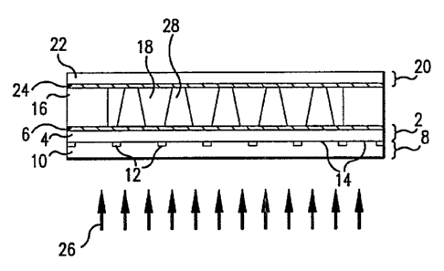
FIG. 6 illustrates exposure of the FIG. 5c binati n to
subs ti y c ' ated light.
FIG. 7' tes the FIG. 6 combination after removal of the
photomask and cover plate.
FIG. 8 tes the removal of unexposed p 1 e' ble
material from the FIG. 7 combination.
FIG. 9' tes the combination res g from FIG. 8.
FIG. 9A ' tes the combination resulting from another
effib ' ent of the present process.
FIG, 10 ' us tes e d exp s e f the FIG. 9c ffibinati ra.
FIG. 11 is exploded sectional view of y f tapered
waveguides with straight sidew s made by the present process.
FIG. 12 is array of tapered waveguides with rectangular
cr ss secti ns viewed in perspective made by the present process.
FIG. 13 is y f tapered waveguides with r dcr ss
secti ns viewed in perspective made by the present process.
W095/13567 2174v 51 PCT/iJS94/11913
7
FIG. 14 is a sectional view of a single tapered waveguide with
straight sidewalls made by the present process.
FIG. 15 is an exploded sectional view of array of tapered
waveguides with curved sidewalls made by the present process.
s FIG. 16 shows an array of tapered waveguides made by the
present process wherein the interstitial regions between waveguides
cont a light absorptive black particulate amaterial.
FIG. 17 shows an array of tapered waveguides made by the
present process wherein the output faces of the wave de array are
i o covered by a transparent protective layer.
FIG. 18 shows an array of tapered waveguides made by the
present process wherein the output faces of the waveguide array are
covered by a transparent protective layer iiicorpora ' g array of
lenses.
escrij!tion of the Preferred E bo i ents
The preferred effibo ' ents of this invention will be better
understood by those of s' in the art by reference to the above
Figures. The preferred eYnbo ' ents of this invention illustrated in the
2 o Figures are not intended to be exhaustive or to t the invention to the
precise form disclosed. The Figures are chosen to describe or to best
expl ' the principles of the invention, and its application and practical
use to thereby enable others s' ed in the art to best u e the
invention.
A waveguide substrate 2 illustrated in G. I is useful in
practicing the present process. Waveguide substrate 2 comprises
substrate 4 and optional adhesion promoting layer 6. At a ' uan,
substrate 4 is tramparent to light widiin the wavelength range from
about 400 to about 700 run, as this visible wavelength region is the
most des ble region in which the optical waveguides to be formed
wiU operate. It is more preferred that the substrate 4 also transmits
ultraviolet light in the region from about 250 to about 400 as this is
the region in which many useful photoinitiators absorb li t.
Additionally, if it is desired to utilize the tapered waveguide array in
the near infrared region, from about 700 to about 2000 , then it
would be preferred to use a substrate 4 which is parent in that
2174851
~
reo-ion as well. The index of refraction of substrate 4 mav range from
about 1.45 to about 1.65. The most preferred index of refraction is
from about 1.50 to about 1.60. Substrate 4 may be made from any
transparent solid material. Preferred materials are commercially
s available and include transparent polymers, glass, and fused silica.
Useful transparent polymers include polyesters, polyacrylates and
methacrylates, polvsty7ene, and polycarbonates. Desired
characteristics of these materials include mechanical and optical
stability at typical operatina temperatures of the display device.
Compared with glass, transparent polymers have the added advantaQe
of structural flexibility which allows products to be formed in larae
sheets and then cut and laminated as necessary. The preferred
materials for substrate 4 are alass and polyester sqch as polyethylene
terephthalate. The thickness of substrate 4 rnay vary widely.
Preferably, the thickness of substrate 4 is about 1 mil (25 microns) to
about 10 mil (250 microns).
Preferably, the adhesion promoting layer 6 is an organic material
which is lio-ht transmissive and causes the waveo-luides to be formed
thereon, especially waveo-ruides formed from polymers as for example
photocrosslinked acrylate monomer materials, to adhere strongly to
substrate 4. Such materials are well known to those skilled in the art,
are commerciallv available, and will not be described herein in great
detail. For example, if substrate 4 is glass and wavegc.iides are formed
from acrylate monomer materials, then an appropriate adhesion
promoting layer 6 may be formed bv reacting the o,lass surface with
certain types of silane compounds includinc, 3-(trimethoxvsilyl)propyl
methacrylate; 3-acrvloxypropyl trichlorosilane; and
trimethvlsilylpropylmethacrvlate. If substrate 4 is polyethvlene
terephthalate (PET) and waveguides are formed from acrylate
3 o monomer materials for exainple, adhesion promotino, layer 6 may be
provided by using an adhesion treated PET film such as Hostaphan
4500 (Hoechst-Celanese). If substrate 4 is emulsion coated and the
wavec-ruides are formed from acrylate monomer materials for example,
adhesion promotino, laver 6 mav be formed from 3-
3 s acry=loxypropyltrichlorosilaile (Huls America A0396). The thickness of
adhesion promotion laver 6 may vary widely. Usually, the thickness of
44-EAtDE~ SH
WO 95/13567 2174851 PCTIUS94/11913
9
adhesion promoting layer 6 is as used in the end application such as
conventional direct view flat panel display devices. In the preferred
eanbo ' ents of the invention, adhesion promoting layer 6 is less than
about 1 lnicrometer thick. If it is dete *ed that adhesion of the
waveguides to a bare substrate 4 is sufficient, then adhesion layer 6
may be omitted.
A photomask 8 as illustrated in FIG. 2 is useful in practicing the
present process. Photomask 8 controls the spatial profile of the
ultraviolet light, that is, where it falls upon the layer of
i o photopolymerizable material. Photomask 8 ffiprises transparent
substrate 10 which has opaque regions 12 and transparent regions 14
on one surface which allow radiation directed at photomask 8 to fall
only on the desired regions of photopol e' ble material. As shown
in FIG. 2A, photomask 8 has a patte of opaque re '0 12 and
is transparent regions 14 which comprise the desired patte of the array
of tapered waveguides. The pattern in Fig 2A is one of many useful
patterns and is intended to be illustrative only. Many other patterns of
transparent and opaque regions are useful the scope of the
present invention. Co erci y available photomasks are useful in
20 the present process.
In the first step of one effibo ' ent of the present invention,
photomask 8 is placed in substantial contact with waveguide substrate
2 as illustrated in FIG. 3. used herein, the term "substantial
contact" means that the photomask 8 and waveguide substrate 2 do not
2 s become separated during the rem ' der of the present process. Any
known method for maintaining substantial contact between two
substrates may be used herein. For example, a liquid such
isopropanol, methanol, or water may be placed between photomask 8
and waveguide substrate 2 and then a rubber roller may be used to
30 press photomask 8 and wade substrate 2 to e er. Other known
methods for maintaining substantial contact between two substrates
include mechanical fixturing, vacuum contact, static contact and others
which enable off-contact or pro ' ty printing, sofl contact printing,
and scanning.
35 In the second step of the first ernbo ' ent of the present
invention, a subs ti y form thickness of a photopol e' ble
WO 95/13567 f'CTY-US94I1Il913
21.7485
mixwre is placed on the waveguide substrate so that the waveguide
substrate is positioned between the photopol e able mixture and the
photomask wherein the photopol e' able mixture comprises a
reactive monomer, or mixture of such monomers, and photoinitiator, or
5 mixture of such photoinitiators, and the photoinitiator is present in an
ainount sufficient to form a gradient of subs ti y co11' ated
ultraviolet light across the thickness of the photopolymerizable nixture
d g a subsequent step. Any known method for placing a
subs ti y uniform thickness of a photopol e ble ffiaterial on a
lo substrate may be used in the present process. - As used herei~, the terrn
"subst ti y uniform thickness" means less than about 10 percent
variation in thickness across the area of the mixture, and more
preferably less than about 5 percent variation in thickness. As will be
expl ' ed 'm more detafl later, the thickness of photopol e' ble
mixtue is the desired final length of a photopol e' ed tapered
waveguide which, in tum, is determined by the minimum tr sverse
distance across the waveguide input surface. Preferably, the length of a
photopol e ed tapered waveguide or the thickness of
photopol e' ble mixture is from about 1 to about 4000 microns,
more preferably from about 15 to about 1600 microns, and most
preferably from about 50 to about 400 microns.
Methods for placing a subs ti y uniform thickness of
photopol e' ble material include spin coa ' g, roller coating, doctor
blading, patch coa ' g using a slot, e ion coating, and the like.
2 s FIG. 4 and 5 ustrate another method. Spacers 16 are positioned on
waveguide substrate 2. The height of spacers 16 is the desired final
length of the photopolymerized tapered waveguide.
Photopolymerizable mixture 18 is then placed on waveguide substrate
2 so that waveguide substrate 2 is positioned between
photopol e' ble mixture 18 and the phot k8.
Photopol e' ble material 18 comprises two essential
ingredients. The first essential ingredient is a photopol e ble
monomer, especi y e ylenic y unsaturated monomer which will
provide a transparent solid polymer material. Preferred solid polymer
3 5 materials have index of refraction between about 1.45 and abo
1.65 and include commercially available pol e y ethacrylate9
WO 95/13567 7 4 E 5 1 PCT/IJS94/11913
11
polycarbonate, polyester, polystyrene, and polymers formed by
photopolymerization of acrylate or methacrylate monomers. More
preferred rnaterials have an index of refraction between about 1.50 and
about 1.60 and include polymers formed by photopolymerization of
s acrylate monomer mixtures composed of urethane acrylates and
methacrylates, ester acrylates and methacrylates, epoxy acrylates and
methacrylates, (poly) ethylene glycol acrylates and ffiet.hacrylates and
vinyl containing org 'c monomers. It is useful to utilize a mixture of
monomers in the photopol e' ble mixture in order to fine time the
i o properties of the composition such as to fine tune cross ' g density,
viscosity, adhesion, curing rate, and refractive index and to reduce
discoloration, crac ' g, and delamination properties of the
photopolymer formed from the composition.
Examples of useful more preferred monomers include methyl
i s methacrylate; n-butyl acrylate (BA); 2-ethylhexyl acrylate (EHA);
isodecyl acrylate; 2-hydroxyethyl acrylate; 2-hydroxypropyl acrylate;
cyclohexyl acrylate (CHA); 1,4-bu e'ol diacrylate; ethoxylated
bisphenol A diacrylate; neopentylglycol acrylate (NPGDA);
diethyleneglycol diacrylate (DEGDA); diethylene glycol dimethacrylate
20 (PEGI3 ); 1,6-hexanediol diacrylate (HDDA); trimethylol propane
triacrylate ( A); pentae tol triacrylate (PETA);
pentaerythritol tetra-acrylate (PETTA); pheno e yl acrylate (PEA); R
-carboxylethyl acrylate ( J3-CEA); isobornyl acrylate ( A);
tetrahydro l acrylate (THFFA); propylene glycol monoacrylate
25 PGA); 2-(2-ethoxyethoxy) ethyl acrylate (EOEOEA); N- ' yl
pyrrolidone (NVP); 1,6-hexanediol dimethacrylate (HDDMA);
triethylene glycol acrylate (TEGDA) or dimethacrylate ( GD );
tetraethylene glycol diacrylate (TTEGDA) or dimethacrylate
( GI) ); polyethylene glycol diacrylate (PEGDA) or
3 o dimethacrylate (PEGDMA); dipropylene glycol diacrylate (DPGDA);
tripropylene glycol diacrylate (TPGDA); ethoxylated neopentyl glycol
diacrylate (NPEOGDA); propoxylated neopentyl glycol diacrylate
(NPPOGDA); aliphatic diacrylate (ADA); alkoxylated aliphatic
diacrylate (AADA); aliphatic carbonate diacrylate (ACDA);
35 trimethytolpropane tiimethacrylate ( ); ethoxylated
trimethylolpropane triacrylate ( EGT'A); propoxylated
WO 95113567 2174851 PC'fl'/1ITS94/41913
12
timethylolpropane triacrylate ( P T'A); glyceryl proxylated
triacrylate (GPTA); tris (2-hydroxyethyl) isocyanurate triaerylate
( ICT'A); dipentae tol pen crylate (DPEPA);
di i ethylolpropane tetraacrylate (D TTA); and alkoxylated
tetraacrylate (ATTA).
Especially useful are mixtures wherein at least one monomer is a
multifunctional monomer such as a diacrylate or triacrylate, as these
will produce a network of crosslinks within the reacted photopol er.
The most preferred materials for use in the method of the invention are
io cross ed polymers formed by photopol 'g mixtures of
ethoxylated bisphenol A diacrylate and timethylol prop etriacrylate.
The index of refraction of the most preferred materials ranges from
about 1.53 to about 1.56. It is not essential that the refractive index of
the transparent solid material be homogeneous throughout the
1s waveguide element. It may be advantageous to cause to be present,
inhomogeneities in refractive index, such as striations or seatte ' g
particles or dom s, as these inhomogeneities may further increase the
divergence of li t from the output of the waveguide array.
The amount of monomer in photopoi e' ble ffiaterial may
20 vaxy widely. The amount of monomer or the total amount of a mixture
of monomers is usuaRy from about 60 to about 99.8 percent by weight
of the photopol e' ble material, preferably from about 80 to about
99 percent by weight of the photopol e ble material, and mo
preferably from about 85 to about 99 percent by weight of the
25 photopol e ble material.
another essential component, the pol e ble material 18
includes a photoinitiator which is activated by actinic radiation to
produce activated species which lead to photo 1 e' tion of the
monomer. The photoinitiator system wiU contain a photoinitiator and
30 preferably a conventional sensi ' er which extends the spectral
response into regio ha ' g spectral u 'ty, e.g. the near ultraviolet
region and the visible spectral regions where lasers excite and where
many co on optical ffiaterials are t-ansmissive. iJs y the photo-
tiator is a free radical-generating addition pol e' tion initiator
3s activated by actinic light and is preferably e y inactive at and
below room teffipera e(e.g. about 20 C to about 25 C.)
WO 95/13567 2174851 FCT/LJS94/11913
13
Illustrative of such initiators are those described in U.S. Patent
No. 4,943,112 and references cited therein. Preferred free radical
initiators are 1-hydroxy-cyclohexyl-phenyl ketone (Irgacure 184);
benzoin; benzoin ethyl ether; benzoin isopropyl ether; benzophenone;
benzidimethyl ketal (Irgacure 651); a,a-diethyloxy acetophenone, a,a-
ethyloxy-a-hydroxy acetophenone (Darocur 1173); 1-[4-(2-
hydroxyethoxy)phenyl]-2-hydroxy-2-Ynethyl-prop -1-one (Darocur
2959); 2-methyl-l-[4-Ynethyl o)phenyl]-2-rnorpho ' o-prop -1-one
(Irgacure 907); 2-benzyl-2- ' ethyl o-1-(4-ffio ho ' ophenyl)-
lo butan- l-one (Irgacure 369); poly (1-[4-(1-ffie yl ' yl)phenyl]-2-
hydroxy-2-ffiethyl-prop -1-one } (Esacure KIP); [4-(4-
ffiethylphenylthio)-phenyl]pheny eth one (Quantacure BMS); di-
campherq ' one; and 50 / 1 -hydroxycyclohexyl phenyl ketone and
50% benzophenone (Irgacure 500).
i 5 The more preferred photoinitiators includes benzidimethyl ketal
(Irgacure 651); a,a-diethyloxy acetophenone; cc,a- ' ethyloxy-a-
hydroxy acetophenone (Darocur 1173); 1-hydroxy-cyclohexyl-phenyl
ketone (Irgacure 184); 1 -[4-(2-hydroxye oxy)phenyl]-2-hy oxy-2-
niethyl-prop -1-one (Darocur 2959); 2- e yl-1-4-
2 (ynethylthio)phenyl]-2-ffiorpho ' o-prop -1-one (Irgacure 907); 2-
be l-2- ' ethyl o-1-(4-rnorpho ' ophenyl) bu -1-one (Irgacure
369); and 50% 1-hydroxycyclohexyl phenyl ketone and 50 /
benzophenone (Irgacure 500). The most preferred photoinitiators are
those which tend not to yellow upon irradiation and, thus, do not
25 increase the coloration of the composition on the Gardner scale to a
value of greater than 8 points on exposure to a temperature of 190 C
for 24 hours dete ' ed by 1544-80. Such photoinitiators
include benzidimethyl ketal (Ir c e 651); a,a,- ' ethyloxy-a-
hydroxy acetophenone (Darocur 1173); 1-hy o-cyclohexyl-phenyl
3 o ketone (Irgacure-1 84); 1-[4-(2-hy o e o henyl]-2-hydroxy-2-
inethyl-propan-l-one (Darocur 2959); and 50% 1-hydroxycyclohexyl
phenyl ketone and 50% benzophenone (Irgacure 500).
The amount of photoinitiator which must be present to form a
gradient of subs tially co ' ated ultraviolet light across the thickness
35 of the photopol e' ble mixture 18 during a subsequent step is from
about 0.1 to about 12 percent by weight based on the total weight of
WO 95/13567 2 17 4 8 5 ?,C7/US94/11913
14
the photopolymerizable rnaterial. The amount of photoinitiator is
preferably from about 0.5 to about 12 percent by weight, and more
preferably from about 0.5 to about 8 percent by weight based on the
total weight of the photopol erizable material. It is re ed that the
desired gradient will be influenced not only by the concentration of the
initiator but by the choice of irradiating wavelengths present in the
exposure source, which may be controlled by those skilled in the art.
In addition to the essential ingredients, the photopol e' able
ffiaterial may include v'ous optional ingredients such stab' ' ers,
lo inhibitors, plasticizers, optical brightners, release agents, ch ' tr sfer
agents, other photopol e' ble monomers, and e' e.
The photopol e' ble material preferably includes a stab' ' er
to prevent or reduce degradation which leads to property deterioration
such as cracking and delamination after heat a'g at 190 C in air for
1.5 24 brs. as de ed by ASTM D 4538-90A and yello g (coloration of
greater than 8 on the Gardner Color Scale as determined by ASTM D
1544-80) after such heat a'g. Such stab' ' ers include UV absorbers,
light stab' ers, and antioxidants.
absorbers include hydroxyphenyl be otriazoles, such as 2-
20 [2-hydroxy-3,5-di(1,1- ' ethylbe 1)phenyl]-2-H-be otri ole
(Tinu ' 900); Poly(oxy-l,2-eth ediyl), a-(3-(3-(2H-be oazol-2
yl)-5-(1,1- ' e ylethyl)-4-hy henyl)-1-oxopropyl)-co-hy oxy
(Tinu ' 1130); and 2-[2-hydroxy-3,5-di(1,1- ' e ylpropyl)phenyl]-2-
H-be o ole ("Tinu ' 238) and hy oxyb ophenones such as 4-
2-9 methoxy-2-hydroxybenzophenone and 4-n-octoxy 2-
hydroxybenzophenone. Light stab' ' ers include hindered amines such
4-hy o-2,2,6,6-te ethylpiperi e, 4-hy oxy-1,2,2,6,6
pen e ylpiperi ' e, 4-benzoyioxy-2,2,6,6-te e ylpiperi ' e,
bis(2,2,6,6-tetr ethyl-4-piperi ' yl)sebacate ('finu ' 770);
3o bis(1,2,2,6,6-pen ethyl-4-piperi ' yl)sebacate (Tinu ' 292);
bis(1,2,2,6,6-pen ethyl-4-piperi ' yl)-2-n-butyl-2-(3,5-di -tert-butyl-
4-hy oxybe i)ffialonate (Tinu ' 144); and polyester of succinic
acid with N-[i-hydroxy-ethyl-2,2,6,6-te e yl-4-hy oxy-piperi ' e
('I inu ' 622). Antioxidants include substituted phenois such 1,3,5-
35 ethyl-2,4,6-tris(3,5-di-tert-butyl)-4-hydroacybe 1)be ene, 1,1,3-
tris-(2-ffiethyl-4-hydroxy-5-tert-butyl)phenyl)bu e, 4,4 -butylidene-
~
WO 95/13567 17485 1 PCTIUS94/11913
bis-(6-tert-butyl-3-methyl)phenol, 4,4'-thiobis-(6-tert-butyl-3-
rnethyl)phenol, tris-(3,5-di-tert-butyl4-hydroxybe 1)isocyanurate,
cetyl-3,5-di-tert-butyl-4-hydroxybenzene (Cyasorb UV2908); 3,5-di-
tert-butyl4-hydroxybeaazoic acid, 1,3,5-tris-(tert-butyl-3-hydroxy-2,6-
5 dimethylbenzyl) (Cyasorb 1790); ste l-3-(3,5-di tert buty1-4-
hydroxyphenyl)proprionate (Irganox 1076); pentaerythritol tetrabis(3,5-
di-tert-butyl4-hydroxyphenyl) (Irganox 1010); and thiodiethylene-bis-
(3,5-di-tert-butyl-4-hydroxy)hydroc ate (Irganox 1035).
The preferred stabilizers used in this invention are antioxidants.
io Preferred antioxidants are selected from subsfituted phenols such as
1,3,5- ethyl-2,4,6-tris(3,5-di-tert-butyl)-4-hydroxybe l)benzene,
1,1,3-tris-(2-methyl4-hydroxy-5-tert-butylphenyl)bu e, 4,4'-
butylidene-bis-(6-tert-butyl-3-ffiethylphenol, 4,4'- obis-(6-tert-butyl-3-
methylphenol, tris-(3,5-di-tert-butyl-4-hy oxybe l)isocy urate,
15 cetyl-3,5-di-tert-butyl-4-hydroxybe ene (Cyasorb LJV 2908); 3,5-di-
tert-butyl-4-hydroxybenzoic acid, 1,3,5-tris-tert-butyl-3-hydroxy-2,6-
ethylbe 1) (Cyasorb 1790); ste l-3-(3,5-di-tert-butyl-4-
hydro henyl)proprionate (Irganox 1076); pentaerythritol te bis(3,5-
di-tert-butyi-4-hydro henyl) (Irganox 1010); and odiethylene-bis-
(3,5-di-tert-butyl-4-hydroxy)hydroc' ate (Irganox 1035). The most
preferred stabilizers include pentae tol tetrabis(3,5-di-tert-butyl-4-
hydro henyl) (Irganox 1010); odiethylene-bis-(3,5-di-tert-butyl4-
hydroxy)hy oc' ate (Irganox 1035); and ste l-3-(3,5-di-tert-
butyl-4-hy o henyl)proprionate (Irganox 1076).
The amount of stabilizers in the composition may vary widely
and is us y from about 0.1 to about 10 percent by weight of the
photopol e' ble material. The amount of s b' ' er is preferably
from about 0.1 to about 5 percent by weight of the photopolymerizable
material and more preferably from about 0.2 to about 3 percent by
weight of the photopol e' ble material.
Cover plate 20 is then placed over photopol e ble mixture
18 and pressed down until it is in contact with spacers 16 as illustrated
in FIG. 5. Cover plate 20 comprises cover substrate 22 and release
layer 24. Cover substrate 22 may be made of any material such as
glass, quartz, fused silica, polymer sheet, or metal sheet. Release layer
W 95/13567 2174V 51 FCTYUS94/11913
16
24 may be a fluorinated polymer such as Teflon AF , a polysiloxane,
or untreated polymer film such as polyethylene terephthalate.
In another embodiment of the present process, wave de
substrate 2 is not used and the photopolymerizable material 18 is
placed directly on photomask 8 (not illustrated).
In the next step of both effibo ' ents of the present process,
while maintaining the photopolymerizable mixture substantially
stationary relative to the substanta y co ' ated ultraviolet light, the
photopol e' ble mixture is exposed through the tr p ent regions
io of the photomask to substantially co ' ated n.ltraviolet light for a time
sufficient to form array of tapered photopol e' ed waveguides
wherei~: (i) the tapered end of each of the waveguides extends
outward from the substrate or photomask, (ii) each of the waveguides
has a light input surface adjacent the substrate or photomask and a light
1s output surface distal from the light input surface, and (iithe area of
the light input surface of each of the waveguides is greater than the area
of its light output surface. The assembly of FIG. 5 is then exposed to
subs ti y co ' ated actinic radiation 26 as ill trated in FIG. 6. As
used herein, the term 'subs ti y coll' ated means that the li t
20 which exits the light source does not diverge from the optical axis of
the exposure system by more than 10 degrees.
The photopol e' ble material is exposed to actinic radiation
of the req ed wavelength and intensity for the req ' ed duration. As
used herein "ac = c radiation" is defined light in the visibl
25 ul violet or infrared regions of the spec , ell electron
bearn, ion or neutron beam or X ray radiation. Actinic radiation may
the form of incoherent light or coherent light, for example light
from a laser.
Sources of actinic light, and e os e procedures, times,
30 wavelengths and intensities may vaxy widely depending on the desired
degree of pol e' tion, the index of refraction of the photopolymer,
and other factors to those of ordinary skill in the art. Such
conventional photopol e' tion processes and their operational
parameters are well known in the art. See for example in S.P. Pappas
s s Ed. "Radiation Curing: Science and Tec olo a Plenum Press, New
York, NY; D.R. Randell Ed., "Radiation Curing of Polymers, U, Royal
WO 95/13567 2174851 PCTIUS94/11913
17
Society of Chenaistry, Carnbridge, Mass; and C.E. Hoyle and J.F.
Kristle, Ed., "Radiation Curing of Polylnelic Nlaterials' , erican
Chemical Society. Accordingly, they will not be described herein in
great detail.
Sources of actinic radiation and the wavelength of the radiation
may vary widely, and any conventional wavelengths and sources may
be used. It is preferable that the photochemical excitation be c'ed
out with relatively short wavelength (or high energy) radiation so that
exposure to radiation no ally encountered before processing (e.g.,
i o room lights) will not prematurely polymerize le pol e' ble
material. Thus, exposure to ultraviolet li t(300-400 wavelength)
and exposure by deep ultraviolet lit(190-300 wavelength) are
preferred. Convenient sources are high pressure xenon or ynerc -
xenon arc lamps fitted with appropriate optical filters to select the
ls desired wavelengths for processing. Also, short wavelength coherent
radiation is useful for the practice of this invention. argon ion laser
operating in the "" mode at several wavelengths near 350 is
desirable. Also, a frequency-doubled Argon ion laser with output near
257 wavelength is desirable. Electron beam or ion beam excitation
20 may also be u'' ed. The most preferred actinic radiation is ultraviolet
light in the 300-400 region, such as produced by a mercury, xenon,
or mercury-xenon lamp.
Substantially co ' ated actinic radiation 26 passes through
transparent regions 14 of photomask 8 and causes a
25 photopol tion reaction in the exposed regions 28 of
photopol e ble mixture 18 which the transparent
regions 14 of the photomask 8 as illustrated in FIG. 6. No, or in some
cases, only limited photoreaction occurs in those areas of
photopol e' ble mixture 18 which are shielded from the
30 subs ti y co ' ated actinic radiation 26 by opaque regions 12 of
photomask 8.
In order that the exposed regions 28 have the proper tapered
shape, the optical absorption of the photopol e' ble mixture 18 at
the wavelengths of the ultraviolet light must be high enough such that a
35 gradient of actinic radiation intensity is established through the film
during ac ' c radiation exposure. That is, the amount of actinic
W 95/13567 21 74rJ 51 l:QCTYi7S94111913
18
radiation available in the photopolymerizable mixtue 18 to cause the
initiation of the photoreaction will decrease from the photomask 8 side
towards the cover plate 20 side, due to the finite absorption of the
photopol erizable mix e 18. This of actinic radiation
causes a gradient in the amount of photopol e' tion reaction that
occurs across the thickness of photopol e' ble mixture 18, and this
results in the unique tapered geometry of the developed waveguide
structures, a geometry which is easily accessible with the process of the
present invention.
The gradient in the amount of photopo e' tion which occurs
across the thickness of photopol e' ble mixture 18 may be further
influenced by the presence of dissolved oxygen gas 'm the
photopol e' ble mixture 18, such oxygen acting to curtail or
quench the photopol e tion reaction except in those areas where
i5 oxygen has been consumed by the free radicals produced 'm the
photopol e' tion process. Such action of dissolved oxygen gas on
the progress of photopol e' tion reactions is well known to those
s' ed in the art. Further, the requisite geometry of the photopolymer
s c es may be further influenced by the process of self focus'mg.
2 o That is, the light f g on the surface of the photopol e' ble
mixture 18 nearest the photomask 8 initiates photopol e' tion at
that surface, and since the refractive index of the solidified polymer
material is higher than that of the liquid monomer, it acts to refract the
light passing through it. this manner, the aerial image of light falling
25 on the photo l e' ble mixture nearer to the cover plate side of the
layer is altered through refraction caused by the already-polymen'zed
material which lies closer to the photomask. This effect may cause a
n o g of the resultant polymerized s c e from the mask side,
upon which the ' a' g light was directed, towards the cover plate 20.
30 In the last step of both eanbo ' ents of the present process, the
photopol e' ble mixture which was unexposed to substantially
co ' ated actinic radiation during the exposure step is removed.
Photomask 8, spacers 16, and cover plate 20 with release layer 24 are
removed as illustrated in FIG. 7. The unreacted monomers are washed
35 away with a suitable solvent 30 such as acetone, methanol, or
isopropanol in a container 32 as illustrated in FIG. 8 leaving a pattem
WO 95/13567 PCBYiJS94/11913
2174851
19
of photopolymerized regions 28 on the waveguide substrate 2.
Depending upon the monomers selected, it may be possible to use
aqueous-based solvents. The remaining final s c e in the first
embodiment of the present invention consists of photopolyrnerized
regions 28 on wavegwde substrate 2 as illustrated in FIG. 9. In the
other ernbo ' ent of the present invention, the pattern of
photopolyr.nerized regions 28 remains on photomask 8 as illustrated in
FIG. 9A. The final s c e containing the array of tapered
photopolymerized waveguides 28 may receive optional post
io development flood exposure to ultraviolet light 34 illustrated in FIG.
to further harden the photopolymer material.
In a commercial batch production ' e, the photomask and
substrate, if used, may be contacted at a first station. This assembly is
then advanced to a second station where a co ated ultraviolet light
source is located. A photopolytne ' ble mixture is placed on the
substrate or photomask and exposed through the transparent regions of
the photomask to the subs tially co ' ated actinic radiation. The
exposed assembly is then advanced to a third station wherein the
photomask and unexposed photopol e ble mixture are removed.
In a commercial continuous production ' e, a
photopol e' ble mixture may be extruded between a flexible
substrate and flexible cover plate (not ' us ted). This assembly then
travels between two rollers wherein one roller comprises a photomask
having opaque and transparent regions thereon and actinic radiation
source situated inside the roller. The photopol e' ble mixture is
then exposed through the transparent regions of the photomask to the
subs ti y co ated actinic radiation. The cover plate is then
removed from the exposed assembly and the exposed assembly
advances around another roller through a solvent bath to remove
unexposed mixture
FIG. 11 shows exploded sectional view of image display
means 36 made of the array of tapered photopol e' ed waveguides
28 shown in FIG. 10. The image display means 36 is composed of the
substrate 4, adhesion promo g layer 6, and array of tapered
dvave des 28. The tapered waveguides 28 have a li t input surface
38, light output surface 40, sidewalls 42 and are separated by
WO 95/13567 2174g 51 PC'1'IUS94/11913
interstitial regions 44 with a lower refractive index than the refractive
index of the wave des. Input surface area 38 of each tapered
waveguide 28 is positioned adjacent to the adhesion promoting layer 6
and is larger than output surface area 40 of each waveguide 28, which
s results in a tapered s c e. The s c e and positio 'g of tapered
waveguides 28 are critical.
As shown in FIG. 11, the area of light input surface 38 of each
tapered waveguide 28 is greater than the area of its light output s ace
40, and the center-to-center distance between light input surfaces 38 of
io adjacent waveguides 28 in the array is equal or subs ti y equal to
the center-to-center distance between light output surfaces 40 thereof,
so that the angular distribution of light effier 'g from light output
surfaces 40 of waveguides 28 is larger than the angular distribution of
light ente ' g input surfaces 38 of waveguides 28. In order that the
is resolution of e age formed by a modulating means such as LCD
(not illustrated) not be degraded as it traverses image display means 36,
it is preferred that the center-to-center distance between li .t input
surfaces 38 of adjacent waveguides 28 is equai to or less than the
center-to-center distance between adjacent pixels of the modulating
20 means. In FIG. 11, sidewalls 42 are shown as straight. However, the
shape of sidewalls 42 may be straight or curved.
The cross-section of a tapered waveguide 28 in a plane parallel
to the surface of image display means 36 may have any shape including
a square, a rectangle, any equilateral polygon, a circle, or oval. FIG.
2 s 12 shows array composed of tapered waveguides 28 with
rectangular cross-sections viewed in perspective. FIG. 13 shows a
similar view of array composed of tapered waveguides 28 which
have circular cross-sections. Examples of shapes for the entire
waveguide 28 include right circular cones, right oval cones, right
square pyramids, and right rectangular pyramids, any of which may be
whole or truncated.
The optical properties, i.e. contrast and change in chromaticity
as a fimction of vie g angle, of array of tapered waveguides 28
are determined by the shape, size, and physical arrangement of the
individual waveguides 28. In FIG. 11, the center-to-center distance
between light input surfaces 38 of adjacent waveguides 28 is equal or
W0 95/13567 21j 485 PC1'/iJS94/11913
21
substantially eqtial to the center-to-center distance between the light
output surfaces 40 of adjacent waveguides 28. Therefore, optical
image entering the array at light input surfaces 38 will be neither
magnified or demagnified after traversing the array.
The tapered optical waveguides 28 of the arrays shown in FIG.
11, FIG. 12, and FIG. 13 are formed from a transparent solid ynaterial
having a higher index of refraction than interstitial regions 44 between
the waveguides. Light rays which enter waveguide 28 through light
input surface 38 (sho in FIG. 11) and thereafter are incident on
io sidewalls 42 of the waveguide at angles greattr than the critical angle
(as defined by Snell s Law) will undergo one or more total inteanal
reflections from the sidewalls 42 and, il~ most cases, emerge from
waveguide 28 through light output surface 40. A few li t rays may
pass through the sidewalls 42 or be reflected back to the li t input
surface 38. The operational fimction of tapered waveguide 28 differs
from a lens in that a lens does not u'' e total internal reflection.
Since waveguide 28 has a taper such that the area of the light
output surface 40 is sffi er than the area of li t input surface 3 8, the
angular distribution of the li t e er g from li t output surface 40
wiR be larger than the angular distribution of the li t ente ' g the light
input surface 38. Image display means 36 ha g array of tapered
waveguides 28 placed at the output surface of amodula g means will
alter the angular distribution of output light from the ffiodula g means
such that the image from the ffiodula ' g means may be viewed at
2 s higher angles. It is preferred that the area of li t output surface 40 of
each waveguide 28 be from about 1 to about 60 percent of the area of
the light input surface 38. It is more preferred that the area of the light
output surface 40 be from about 3 to about 40 percent of the area of the
light input surface 38. It is most preferred that the area of li t output
surface 40 be from about 4 to about 20 percent of the area of li t input
surface 38.
In order that image display means 36 has high overall light
throughput, it is preferred that the sum of the areas for all wave de
light input surfaces 38 be greater than 40 percent of the total area of
substrate 4 of the array. It is more preferred that the sum of the areas
for all waveguide li t input surfaces 38 in image display means 36 be
Wo 95/13567 2174851, ?C.1.IUS94/11913
22
greater than 60 percent of the total area of substrate 4 of the array. It is
most preferred that the sum of the areas for all waveguide light input
surfaces 38 il~ image display means 36 be greater than 80 percent of the
total area of substrate 4 of the array.
The index of refraction of interstitial region 44 between the
tapered waveguides 28 must be less than the index of refraction of the
tapered waveguides 28. Preferred materials for interstitial regions
iriclude air, with index of refraction of 1.00, and fluoropolymer
materials with index of refraction ranging from about 1.30 to about
1.40. The most preferred ffiaterial is air.
A single tapered wave de 28 with light input surface 38, li t
output surface 40, and straight sidewalls 42 is shown in FIG. 14. If
tapered straight sidewalls 42 in the dra ' g are extended until they
intersect, they form taper angle 46. Desired values for taper angle 46
1 5 range from about 2 degrees to about 14 degrees. More preferred
values for taper angle 46 range from about 4 degrees to about 12
degrees. Most preferred values for taper angle 46 are from about 6
degrees to about 10 degrees.
The length 48 of tapered wave 'de 28 depends upon dimension
50 which is the minimum transverse distance across wave de light
input surface 38. For example, if light input surface 38 has the shape of
a square, diinension 50 is the length of one side of the square. If li t
input surface 38 has a rectangular shape, dimension 50 is the smaller of
the two side dimensions of the rectangle. The specific values for
2 s dimension 50 may vary widely depen ' g on the center to center
distance between adjacent pixels of a modulating means. In order that
the resolution of the image formed by a moda g means not be
degraded, dimension 50 should be equal to or less than the center to
center distance between adjacent pixels of a modulating means. For
3 o example, if the center to center distance between adjacent pixels in a
rnodula ' g means is 200 microns, then dimension 50 is gener y in the
range from about 5 microns to about 200 microns, more preferably
from about 15 microns to about 200 'crons, and most preferably from
about 25 microns to about 100 microns.
35 Once dimension 50 is chosen, length 48 may be specified by the
ratio of length 48 to dimension 50. The ratio of length 48 to dimension
2174851
WO 95113567 PCT'/L7S94/11913
23
50 may vary widely depending on how much one wishes to increase
the angular distribution of light emerging from the light output surface
40 compared to the angular distribution of light entering input surface
38. The ratio of length 48 to ditnension 50 is usually from about 0.25
to about 20. It is more preferred that the ratio of length 48 to
ditnension 50 be from about I to about 8. It is most preferred that the
ratio of length 48 to dimension 50 be from about 2 to about 4.
A further embo ent of the present invention is illustrated in
FIG. 15. Image display means 36 is composed of a substrate 4, an
io adhesion promoting layer 6, and individual tapered waveguides 28.
Waveguides 28 have curved sidewalls 52 instead of straight sidewalls
as was shown in FIG. 11. The preferred relationships between the area
of the light output surface 54 and the area of the light input surface 56
are the same as the preferred relationships previously stated for tapered
waveguides 28 with straight sidewalls. In particular, it is preferred that
the area of light output surface 54 of each waveguide 28 be from about
1 to about 60 percent of the area of light input surface 56. It is more
preferred that the area of the light output surface 54 be from about 3 to
about 40 percent of the area of light input surface 56. It is most
preferred that the area of li t output surface 54 be from about 4 to
about 20 percent of the area of light input surface 56.
A preferred elnbo ent of the present invention in which the
interstitial regions 44 between tapered waveguides 28 are fdled with a
light absorptive material, as for example li t absorptive black
particulate material 58 is shown in FIG. 16. By u'' g a light
absorptive material in interstitial regions 44, the direct view display
device has higher contrast and less ambient light is reflected back to the
observer. It is preferred that li t absorptive particles 58 be used for
the interstitial regions 44 rather than a con ' uous black ffiaterial in
order to minimize the area of black material in contact with sidewalls
42 of the waveguides. A continuous black material in interstitial
regions 44 would result in excess absorption loss to li ttr n.iitted
through waveguides 28. Any light absorptive material can be used to
form light absorptive black particles 58. These materials can be
identified by a black color.
W 95/13567 2 174~ 51 ?C'r/1TS94111913
24
Examples of useful light absorptive black particulate material
include carbon lampblack powder, mixture of carbon black and toner,
and rru'xture of carbon black and fluoropolymer. Loo g at the light
output side of array of tapered phot pol e ed wave des, the
light absorptive black particulate material causes the array to appear a
dark matte black and provides good light trans ssion and little
reflection.
In one enlbo ' ent, light absorptive black particulate aterial 58
is confined to interstitial regions 44 between waveguides 28 by us'mg a
io low index polymer having light absorptive blAck particulate ffiaterial
therein. It is possible to make suspensions or emulsions of li t
absorptive black particulate rnaterial. In these cases, the c'er
ffiaterial for the black particles should preferably have index of
refraction less than the index of refraction of the individual tapered
waveguides. This lower index fiUing material allows for total internal
reflection (tir) of light propagating through the tapered wave des to
occ . It is more preferred that the index of refraction be at least 0.1
units less than the index of the preferred tapered waveguide material.
It is most preferred that the index of refraction be 0.2 units or more less
than the ir~dex of the preferred tapered waveguide material. For
example, a suspension of amorphous teflon, such Teflon
available from DuPont Corporation, and carbon lampblack powder 'm
solvent may be coated onto an array of tapered photopol e ed
wave des. The solvent is then evaporated and the teflon acts
2-5 optical buffer. another ex ple, emulsion of fluoropolymer and
carbon lampblack powder in water may be used. In another example, a
low index fluo ated polyurethane resin mixed with carbon lampblack
powder may be used. The light absorptive black particulate material
mixtures are typicaUy cured by heating or and after curing, the
surface may be cleaned by buffing.
A further effibo ' ent of the present invention shown in FIG.
17 which incorporates protective layer 60 over output ends of the
tapered waveguides 28. Protective layer 60 prevents mechanical
damage to the output surfaces of waveguides 28 and also se es to
confine li t absorptive particulate material 58 to interstitial regions 44
between waveguides 28. Protective layer 60 may be ex ded or
CA 02174851 2004-05-03
laminated overcoat. A protective layer may also be applied to the
output surfaces of waveguides 28 before filling the interstitial regions
44 with a light absorptive black particulate material 58. Protective
layer 60 is composed of a transparent backing materia162 as for
5 example the material used to form substrate 4 and optionally and
preferably anti-reflective film 64 formed from a material such as
magnesium fluoride, which reduces specular reflections of ambient
light from the surface of image display means 36. An anti-reflective
coating may also be evaporated directly on the light output ends of the
io tapered waveguides 28 and interstitial regions 44. Examples of useful
anti-reflective coatings are the fluoropolymers taught by commonly
assigned U.S. Patents 5,061,769; 5,118,579; 5,139,879; and 5,178,955
to Aharoni et al.
In FIG. 18, an embodiment of the present invention is illustrated
s..s which utilizes a protective layer 66 which includes an array of negative
lenses 68. Each lens 68 is formed on substrate 70 and is aligned with
the light output end 40 of tapered waveguide 28. Lens 68 is composed
of a material with a lower refractive index than the overcoat layer 72.
The advantage of incorporating an array of negative lenses with the
20 image display means 36 is that the resulting display will have increased
viewing angle.
The array of tapered waveguides produced by the present
process may be used as image display means- in the direct-view flat
panel display devices of commonly assigned U.S. patent application
25 panel display devices of U.S. Patent Number 5,481,385.
Such display devices are used in computer terminals,
televisions, airplane cockpit displays, automotive instrument panels,
and other devices that provide text, graphics, or video information. In
addition, the array of tapered waveguides produced by the present
process may be used to alter or improve the optical characteristics of
other information displaying means such as road signs, cathode ray
tube (CRT) displays, dead front displays and other text, graphic or
video information displays which do not fall in the category of flat
panel devices, or to alter or improve the brightness or optical
characteristics of lighting systems.
W 95/13567 2 ~ ~ ~ 851 PCT/LTS94/11913
26
In an altemate method for co ercial production, the
photochemical m ac g process described above may be used i~
srriall scale to produce tapered waveguide masters. The tapered
waveguide master may then be used to create inverted tapered
waveguide mold. The process for making such an inverted tapered
waveguide mold is well known to those skilled in the art (see e.g.
chael T. Gale et al., "Con ' uous-relief Di active Optical Elements
for Two- ' ensional Array Generation" in Applied Optics, Vol. 32,
No. 14, p. 2526 (1993)). Typically, the mold is made by electroless
io depositing nicke l metal. From this mold, further metal molds may be
fabricated. Each successive mold generation provides the opposite
profile pol 'ty from the previous mold. Manufacture of the tapered
waveguides may then be carried out by fiUing a mold of opposite
profile polarity from the master with a photopol e' ble mixture and
1s exposing the mixture actinic radiation. The resulting s cture is
then separated from the mold and is a subs ti y exact replica of the
ori al tapered waveguide master. The replicated s c e can be
made free standing or can be created on a subs te, such as glass or
polyester filni, by applying the substrate to the photopol e able
20 mixtue and mold before pol e' tion. A decision to employ the
replica from a mold technique wiR be guided by the exact dimensions
of the waveguide array being fabricated as well the production scale.
The subsequent steps described in this process can now be applied to
either the ori al or replicated tapered waveguide arrays.
25 The f o g specific examples are presented to particularly
us te the invention and should not be construed to place limitations
thereon.
E PLE I
30 The production of array of tapered waveguides on a thin,
plastic film was achieved and was most desirable because of both its
diinness and econo 'cs. A photolitho phic y created mask
(5"x5 Bx0.09 ) with a two- ensional d of 45 micron wide clear
squares on 50 cron centers was used. The 5 'cron wide spaces
3 s between squares were opaque to ultraviolet and visible radiation. Onto
this mask a few drops of methanol were applied and then a 100 ffiicron
2174851
27
thick poly(ethylene terephthalate) (PET) film was pressed on. This
PET film was prepared with an ultra-thin film surface treatment which
renders it reactive and adherable to polvmerizing monomer solution.
Such surface-activated films were known to those skilled in the art.
The surface tension of the methanol caused the film to mildlv, but
firmlv adhere to the mask. The mask and the surface-activated PET
film constituted the arrav substrate subassemblv.
Onto a separate 12.7 cm x 12.7 cm x 0.64 cm blank glass plate
was bonded a PET film usinQ a pressure sensitive adhesive. This
o constituted the release fihn subassembly. The release film subassexnbly
was placed fi1m-side up on a black, metal platform containing threaded
holes. Metal spacers, 1 cm x 3 cm x 200 microns thick, were placed
around the edges on top of the release film. Approximatelv 1 rni.ll.iliter .
of a photopolymerizable monomer solution was delivered to the center
of the release film. This monomer solution consisted of 62 parts
ethoxylated bisphenol A diacrylate; 31 parts trimethylolpropane
triacrvlate; 1 part pentaerythritol tetrabis(3,5-di-tert-butyl-4-
hvdroxyphenvl) (Iraanox 1010) antioxidant; 2 pa.rts a,a-dimethyloxy-a
-hvdroxy acetophenone (Darocur 1173) photoinitiator; 2 parts
2o benzidunethyl ketal (Irgacure 651) photoinitiator; and 2 parts of 50%
1-hvdroxvcyclohexyl phenyl ketone and 50% benzophenone (Irgacure
500) photoinitiator. The array substrate subassembly was then placed,
PET fihn-side down on top of the monomer solution. A clear glass
12.7 cm x 12.7 cm x 0.64 cm plate was placed on top of this entire
fabrication assemblv and metal clamps and screws were used to fully
and evenlv compress the plates tolgether resulting in a 200 micron thick
monomer solution layer between the release film and the array
substrate.
At this point the entire fabrication assembly was placed under
the collimating lens of a ultraviolet/visible (TJV-vis) radiation exposure
system. The UV-vis system contained a 1000 Watt Mercury-Xenon
lamp and delivered even, collimated, and homogeneous full-spectrum
radiation with an intensity of 85 mW/cm2 to the entire 12.7 cm x
12.7cm area of the fabrication assembly. The sample was irradiated for
3s 0.76 seconds. The fabrication assembly was then disassembled and the
PET film with the array of tapered optical waveguides now formed, but
still covered with monomer solution in the interstitial regions between
elements, was
ENDE-9 5i
wO 95/13567 2174851 PC'T/1J594/11913
28
positioned upside-down in a bath of isopropanol and left for ten
minutes. Isopropanol was a relatively poor solvent for the monomer
but was advantageous since it allowed for the even and mild
development of the optical waveguide elements' reflective walls. After
s removal of the residual monomer, the tapered optical waveguides were
dried in a stream of nitrogen gas, placed in a a nitrogen gas-purged
enclosure, and hard cured under the UV-vis radiation for an additional
20 seconds.
Electron microscopy and optical microscopy were used to
io evaluate the tapered optical waveguides. The-individual optical
waveguides were observed to have the shape of cated right square
pyr ds. The elements were 200 microns tafl. The width of the
smaller, output surface of the optical waveguides was 20 microns. The
reflective sidewalls were very smooth and joined together at a depth of
15 160 microns below the output surface face. The input surface of the
waveguides was located at the interface between the 100 micron thick
PET array substrate and the width of this input surface was 50 microns
although, as described, the input surfaces were to y fused together in
this example. The taper angle of the optical waveguides was thus 12
2 o degrees.
EXAMPLE II
Example I above was taken as a starting point. The tapered
optical waveguides were abundantly covered with carbon lampblack
25 powder, an optic y absorbing mateiial. The lampblack powder had a
average particle size much smaller than the 50 micron dimensions of
the optical waveguides. The powder was then care y smoothed into
the interstitial regions of the array of tapered optical waveguides using
a soft instrument, in this case a gloved finger. The excess was removed
30 with the same ins ent. The optical waveguides were so robust that
the lampblack could be spread without causing visible damage.
Loo ' g at the output side of the tapered waveguide array, the
lampblack caused the array to appear a dark, matte black. The percent
of the visible surface area which was blackened was determined to be
35 85 percent.
2 17~~51
WO 95/13567 PC'r/CJS94/11913
29
A transmission measurement was carried out by passing a
helium-neon laser beam with a gaussian mode shape and a 6 degree full
divergence angle through the array of tapered optical wave des.
When the light propagated from the light input side towards the light
output side of the waveguides, the transffiission was 60%.
A further experiment was c'ed out on a separate array of
tapered optical waveguides. Here half the array was filled with
lampblack powder and the other half was flUed with a black liquid
epoxy. After the epoxy dried, the two samples were compared. The
io array area f.lled.with lampblack when viewed from the light input side
appeared very transmissive and the array exhibited a snlission of 60
percent from the light input side to the light output side. The array area
filled with black epoxy when viewed from the li t input side appeared
much less transmissive and the array exhibited a s ssion of about
i 5 15 percent from the light input side to the light output side. This
showed that the choice of optically absorbing material was very critical
in allowing light to propagate success y through the array of tapered
waveguides. Where the optically absorbing material was lampblack
powder, the powder came in direct contact with only a syn fraction of
20 the surface area of the waveguide sidewalls and allowed the
phenomenon of total internal reflection to proceed unimpeded. Light
was transmitted through the waveguides by entering the input ends of
the waveguides, reflec ' g off the side w s of the waveguides, and
exi ' g through the output surfaces. When the optically absorbing
25 material was a black epoxy, its index matched to the reflective
sidew s and caused the light to couple through the sidew s and be
absorbed by the optically absorbing material.
EXAMPLE III
30 Example II above was taken as a starting point. The array of
tapered optical waveguides with interstitial regions ed with
lampblack powder was laminated together with a piece of PET film
prepared with a pressure sensitive adhesive. The pressure-sensitive
adhesive formed index matched interface with the output surface of
35 the optical waveguides. The array of waveguides con ' ued to show a
sffiission of 60 percent as irz Example II above. The array of tapered
W095/13567 211 4' 1 PC'A'/US94/11913
optical waveguides was now fitted with a protective layer and was
washed, flexed, and handled without damage to the waveguides and
without loss of the powdery, optically absorptive ffiaterial.
5 EXAMPLE IV
Example II above was taken as a starting point. The array of
tapered optical wave des with interstitial regions fifled with
1 pblack powder was 1 ' ated together with a piece of plastic heat-
activated lamination film, typically used to laminate iden ' cation
io cards. The laminating film formed an index tched interface with the
output surface of the optical wave ides. The array of waveguides
continued to show a transariission of 60 percent as in Example H above.
The array of tapered optical waveguides was now fitted with a
protective layer and was washed, flexed, and handled without damage
15 to the waveguides and without loss of the powdery, optically
absorptive material.
EXAMPLE V
Example IV above was taken as a starting point. When viewed
20 from the light output surface, the laminated, protectlve fLbn offered a
con ' uous air-plastic interface which caused light from be ' d the
viewer to be reflected back into the viewer's eye. The example was
covered with a layer of the same photopol e' ble monomer solution
as used in Example I above. top of the array and monomer solution
2.5 was then placed a glass plate with ti-reflection coating. After
c g the monomer solution with -vis radiation, the array of
tapered optical waveguides with a protective, laminated plastic film,
and a further anti-reflection coated glass plate was observed to appear
much darker. This was due to the reduction in reflected spurious li t
3 o reac ' g the viewer's eyes.
EXAMPLE
Example IV above was taken as a starting point. The protected
array of tapered optical wave 'des with absorptive black material was
placed in front of a helium-neon laser beam a gaussian mode
shape and a 6 degree fuU divergence angle. The laser beam propagated
Wo 95/13567 21748 51 PC'I'IiJS94111913
31
from the light input side to the light output side. The light output was
then observed on a diffusive viewing screen to be transformed into a
broad pattem. This pattern was analyzed using video frame grabbing
instrumentation and computer software. Analysis showed that this
array of tapered optical waveguides caused light to be transformed into
a broad output pattern centered about the central laser beam spot. Due
to the use of a single laser beam and the geometry of the waveguides,
the output pattem contained four-fold s etry and 8 spots of roughly
equal intensity. The full angular distribution of the regions of
lo maximum spot intensity was 40 degrees. The entire output pattem of
the array of tapered waveguides showed a relatively smoothly
decreasing variation in light output intensity over a ftffl angle of about
60 degrees even though the laser beam input had only a 6 degree
divergence. J
A lambertian diffuser offered an object to test the absolute
display characteristics of the array of tapered optical waveguides. The
intensity of the light propagating co early with the laser beam was
norrnalized to 1. At a full angle of 40 degrees, the array of tapered
optical waveguides provided 50 percent of the intensity of the ideal
lambertian dfffuser. At a full angle of 60 degrees, the array of tapered
optical waveguides provided 17 percent of the intensity of the ideal
lambertian diffuser. It should be pointed out that the 1 bertian
diffuser operates by a anech isffi of intense scattering and transmitted
only 47 percent of the light incident on one surface in the forward
2 s direction.
EXAMPLE VII
Example I was taken as a starting point. A blackfillin g mixture
was created by mixing 5 parts carbon lampblack (Degussa
Corporation) with 20 parts Fluorolink-T, 80 parts Fluoro '-B (from
Ausimont Corporation), and 0.005 parts hardener, dibutyl tin dilaurate.
This fluorinated polyurethane mixture had an index of refraction of
about 0.2 units less than the index of the photopolymer tapered
waveguides. This mixture was then applied to the interstitial regions of.
the tapered waveguide array with a soft ent, in this case a
gloved finger. The excess was removed by using the same instrument
WO 95/13567 2 174851 PC'1y1I7S94/11913
32
and also was cleaned with blotter paper. The top surface of the cones
were observed to be clear of the black mixture. The array of tapered
optical waveguides with interstitial regions filled with the blac ing
mixture was then allowed to cure in an oven at 50 degrees Celsius for 2
hours.
Looking at the output side of the tapered wave 'de arrav, the
blac g mixture caused the array to appear a dark, matte black.
The percent of the visible surface area which was blackened was
dete ed to be 85 percent.
A transni*ssioal measurement was carried out by passing a
heli -neon laser beam with a gaussimode shape and a 6 degree fiffl
divergence angle through the array of tapered optical wave des.
When the light propagated from the light input side towards the light
output side of the waveguides, the trans 'ssion was 57%.