Note: Descriptions are shown in the official language in which they were submitted.
wo gS/12047 PCT~US94n2498
21 7~937
-- 1 --
ELECTRONIC COMBINATION LOCK
DESCRIPTICN
Technical Field
The invention relates to the electror~ic I Iocks. More specif~cally, the
5 invention relates to electronic; h;n-~tir~n locks in which an assembly of '
elements and . . ;~ t d processes provide a wide range of features.
Back~round Art
Various lock designs are known in the art. Cu~ ally, locks have been purely
0 n~rh~nir~l in design. However, with the d~,~.,lu}~ of reliable integrated circuits and
vl v~ more s~ ' and functional lock devices have become possible.
However, even historicaUy )I' ' electronic lock designs have failed to provide a
number of desirable features.
Desirable features include the ability to be self-powered, so that correct operation
15 of the lock is not prevented during power failures or battery failures. Whereas certain self-
powered loclcs are known in the art, their designs suffer from the possibility that the self-
charging function can interfere with the ' entry function.
Also, it is desirable that locks be tamper-evident and resistant to physical attack
Also, it is desirable to reduce tbe number of ~- r ' in a lock, so as to enhance
2 0 simplicity and promote reliability. Known locks have not adequately reduced the number
of, . such as in the . used for bearing and retaining a c~
dial, or in a mechanism used to act directly on the linkage to the bolt. Typically, known
locks have involved gears which are '~ comple~c and prone to failure.
WO 95/12047 PCTIIIS94112498
.
2~14931 - 2 -
n is also desirable to avoid a situation in which a user enters a correct . ~
and tbus enables the bolt to be withdrawn, but for some reason leaves the lock unattended
so that some other, ' ' individual may open the lock. It is desirable to prevent
an, ' person from opening the lock after the authorized person, who entered a
5 correct . ' has departed.
Along a similar line, especially pertinent to self-powered locks which have a limited
power storage capacity, it is desirable to ensure that there is sufficient energy to prevent
any person from opening the lock if there is not enough power to operate the lock
correctly. However, C()~ ....iUllal locks have overlooked these features.
It is especially desirable in self-powered locks to use ~ . which consume
a minimum amount of power. Among the r ' of co-~, ' locks which
'~, consume power are the sensors which sense motion and rotation of the
.,.l,:.";,~. dial. Cu..~ ' lock designs have overlooked a feature of reducing
y power A '- in this a~ea
It is also desirable to provide a cnn~hin~inn lock in which, after a person has
entered a given number of . ' which are incorrect, it is made even more difficult
for the user to open a lock. This feature is based on the premise that an
individual (or a rapid dialling machine) attempting to open the lock without knowing tbe
correct c~ml will first enter several ' incorrectly. However,
2 0 ~u..~ ' lock designs have not . ' ' this desirable feature that, based on an
apparent attempt by an - ~ user to open the lock, it should be made even more
difficult for the user to open the lock.
Thus",u..~. ' lock designers have overlooked many features, and cnml
of features, which would provide a versatile, convenient, tamper-evident, reliable, power-
WO 95/12047 2 1 7 4 q 3 7 PCTleJS94112498
efficient, electronic . hiro-inn lock. It is to meet these demands that the present
invention is dioected.
DISCLOSUR13 OF INV~NTION
The present invention provides a variety of featuoes which overcome limitations of
known locks, including electronic cnnrhino~inn locks.
According to a first aspect of the invention, a dual dial r~rrr~ is provided,
including a first dial which is turned to generate power, and a second dial which rotates to
generate numbers to oepoesent the dial position. As an additional feature, the second dial
can be pushed to input a selected displayed number as a ~ n ~ entry.
Thus, the invention provides an ~ of controls on a t nmhit~inn lock, the
,, comprising means for I r~ a c~ and for allowing opening of
the lock, when power is provided, means for storing and providing power to the
Ir~ means, a first control structure7 accessible from outside the lock, which ismovable by a user to provide power to the storing means, and a second control structuoe,
accessible from outside the lock, which is movable by the user separately from the first
control structure to determine the ~
According to a second aspect of the invention, means aoe provided for oetaining the
first and second dials, which function both as bearings for the dials, and as oetaining
2 0 members for the dials, so that the cnmhinotinn lock is tamper-oesistant and tamper-evident.
Thus, the invention provides an ~ for bearing and oetaining at least one
e~ternally accessible rotatable dial on a ' Iock The ~ ~ comprises a
support structure, the rotatable dial, and an integral l,r~uih.~ g member, affL~ed to
a first one of the support structuoe or dial, the member including a clip which matingly
WO 9~/12047 PCTIUS94/12498
37
engages a slot in a second of the support structure or dial so that the clip cannot be
removed from its mating . ~ with the slot without causing visible damage.
According to a third aspect of the present invention, a motor,7ed cam directly acts
on a locking lever, so that the lock bolt is mPrl~lir~lly drawn by the lock dial.
Thus, the invention also provides an within a lock" . - a
motor, a motor cam which is directly responsive to turning of the motor, a bolt which is
extendable out of and w;~l~dlaw~l~ into the lock, and a locking lever which is operatively
connected to the bolt and which is directly contacted by the motor cam and directly
responsive to the motor cam so as to be moved into and out of an "engage" position in
which tne bolt may be extended or withdrawn from the lock.
According to a fourth aspect of the present invention, a timeout period is provided
after a correct L' '' has been entered. If the bolt has not been withdrawn during
the timeout pedod, the invention prevents it from being withdrawn, umtil a correct
has again been entered.
Thus, the invention further provides an within a lock, comprising a bolt
capable of being extended from or withdrawn into the lock, means for entering an input
,.. 1.: .-;.,.. and a controller. The controller includes means for comparing the input
.. with at least one correct crmhi~qti~n and for ,'~ ' g a match
h. ~.., means for forming a time window after the match is ~' d, amd means
2 0 for enabling the bolt to be withdrawn only during the time window.
A flfth aspect of the invention provides a scheme of monitoring power supply
voltages witbin the lock. For example, if -~ power is available to operate the
Iock, the monitoring feature prevents the lock from attempting to opeMte at all. PrefeMbly,
W095/lZ047 2 ~ 7 4 9 3 7 PCTrl~S94rl2498
tbis monitoring is performed in a flexible manner using a ~ ull~ such
as one including a Illi-,lU~ ,~Vl CPU.
Thus, the invention also provides a self-powered lock comprising a bolt capable of
being e~ctended from and withdrawn into the lock, and means, responsive to entry of a
5 correct, ll;nqtj~n for enabling the bolt to be withdrawn into the lock. The, the
enabling means has an "engage" position in which the bolt can be withdrawn into the lock
and a "disengage" position in which the bolt cannot be withdrawn into the lock. The lock
also has means for storing energy for operation of certain ~ the lock, means for
monitoring an energy level of the storing means, and means, responsive to the monitodng
10 means, for preventing the enabling means from moving from its "disengage" position to its
"engage" position if the monitored energy level is below a given energy threshold. The
given energy threshold is greater than or equal to an amount of energy required to
ly move the enabling means from its "engage" position to a "disengage" position
after a i ' ~ ' time period.
According to a sixth aspect of the present invention passive magneac sensors are
used to sense movement of a dial, and, in ~ with other circuitry, determine the
direction of dial movemenL
Thus, Lhe invention further provides a self-powered lock compdsing a movable dial,
accessible from outside the lock for a user to select am input ~ ' means for
20 generating and storing energy, a ,..~g.. i;- d element, moving in response to the dial's
movement, a Wiegand sensor placed with respect to the ~ ' element for generating
signals indicative of movement of the ~ - d element, and a controller, powered by
the energy from the stodng means, for i-~ I;..P the signals from the Wiegand sensor
and for controlling operation of the lock.
WO 95/12047 PCTNS94/12498
~ 7 4937
According to a seventh æpect of the present invention, after a given number of
~tu~ entered, incorrect ~ have been made, a "lockout state" is entered
in which the lock is prevented from opening, even if a correct ' is entered. An
"override" c~ is provided to end the lockout state.
Thus, the invention provides a .~ lock capable of operating in (1) a
normal mode in which at leæt one first c ~ . allows the lock to be opened and (2) a
lockout mode in which at leæt one second c~ allows the lock to be opened,
wherein the at leæt one first . . ~ differs from lhe at leæt one second ~
The lock comprises means for receiving an input ~Amhin~ti~n means for comparing the
input, ' with the at leæt one first o~ means for counting a number of
"u~ entered incorrect input ~ which do not match a valid first
1 and means, responsive to the counting means when the counting means
determines that a given threshold number of :~u~.c.~,~o;~,ly entered incorrect cnml
have been F o ' e~l for changing the operational mode of the lock into the override
mode.
According to still another æpect of the present invention, power storage for DC
operation of various c~. ,t.~ of a lock are separated, so that available power for a
given function may be monitored, and selected monitored power depletion may thus govern
operation of the lock.
According to still another æpect of the invention, data is sent serially from a
processor to a ~ tj.." number display, to minimize the number of pathways pæsingthrough the door of the security container.
WO 95J12047 PCT/US94/12498
21 7~937
-- 7 --
According to a further aspect of the invention, switches which detect bolt position
and the position of the dial which is pushed to choose ' numbers, are providedwith pivot posts and overtravel springs, to minimize damage to the switch case.
Other objects, features, and advantages of the invention will be apparent to those
skilled in the art, upon reading the following Best Modes for Carrying out the Invention
in ~ with the . .~ ~ drawing figures.
BRIEF DESCRIPI ION OF DRAWINGS
The invention is better understood by reading the following Best Mode(s) for
Carrying out the Invention with reference to the . ~ g drawing flgures, in whichlike reference numerals refer to like elements throughout, and in which:
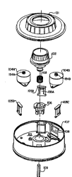
FIG. 1 is an exploded p~ . view of a dial assembly according to a preferred
Pm~~ ' of the present invention.
FIG. 2 is an exploded p~ view of a ~ock ~ according to a
preferred Pm~
FIG 3A is a circuit diagram illustrating preferred, ~- " of circuitry for
prodncing power levels, power sensing levels, and other signals used in an ~ I,o~l ' of
the electronic ' lock.
2 0 FIG. 3B ~ h ~ ly illustrates a central processing unit (CPU) receiving rotational
~f~ from a rotating dial and other ~ regarding power levels, and
controlling a display and motor cam, thus clc~ ullically governing operation of an
P~-' of the electronic: hi~ iOn lock.
FIG. 4 illustrates a preferred drive cam 218 (FIG. 2), showing details thereof.
WO 95/12047 PCIIUS94/12498
~7~937 - 8 -
FIG. S is an enlarged view of the locking lever 213 (E71G. 2), with FIGS. 5A and
SB showing relative orientation of the motor cam 205 in relation thereto in the engage and
disengage (lock) position.
FIG. 6 is a flow chart illustrating single user operation of the preferred electronic
5 . ' Iocl~
FIG. 7 is a flow chart ;,,.I,l,l., . ll;,~g the flow chart of FIG. 6, illustrating the
"lockout" state enhred when a user has entered a given number of incorrect ct)mhin~tir~nc
FIG. 8 - ' 'ly illustrates various elemenfs from FIG. 1, not necessarily to tbe
same scale, to ~ mr the tamper-eYident features of the present invention.
BEST MODE(S) FOR CARRYING OUT THE INVENTION
In describing preferred ~, ho.l;, .. ~f~ of the present invention illustrated im the
drawings, specific ~.l.lil~olo~y is employed for the sake of clarity. However, the invention
is not intended to be limited to the specific h~lfillolo~y so selected, and it is to be
understood that each specific element includes all technical equivalents which operate in
a similar manner to accomplish a similar purpose. For example, the terms "uppern,
"lower", "aboven, "below", "clockwisen, "counter-clockwise", and the like, are used for
purposes of explaining a preferred emhoflim(~nf illustrahd in the ~,~ . Jillg drawings,
but should not be interpreted as limiting the claims which follow this ~
2 0 FIG. 1 illustrahs in exploded perspective view a preferred dial assembly according
to the present invention.
A dial ring 10.7 houscs and supports the elements of the dial assembly. An outer
dial 101 is positioned ~" ~ lly atop the dial ring, and is supported on it by three
bearings, illustrated as elements 105A, 105B, and 105C The bearings, coll~ ly referred
WO 95/12047 PCT/US94/12498
21 74937
g
to herei~ as element 105, fit in an annular slot (not visible in FIG. 1) in the bottom side
- of outer dial 101. The bearings 105 are provided vith retaining clips, which may be leaf
springs, one of which is visible in FIG. 1, as element 155A. Bearings 105 are first retained
in the dial ring 107, and outer dial 101 snaps into place. As the outer dial snaps into place,
5 tbe bearings fit in the annular slot in the bottom of the outer dial, snapping in place through
the action of retaining clips 155A. FIG. 8 illustrates the details of tbis ~, in
greater detail.
Thus, after the outer dial is snapped in place, the lock ' is less susceptible
to physical attack, as the dial is retained by its bearings. Should an individual forcibly
10 remove the dial after it is mounted on the bearings, the bearings and dial would be visibly
damaged, leaving evidence of the attempted entry or vandalism.
The invention also provides one or more generators 104A, 104B, which are secured
to the dial ring 107. Tbe generators 104A, 104B are provided with respective rotary gear
members 154A, 154B. Teeth on the periphery of gear members 154A, 154B interlock with
15 an annular gear (not shown) on the bottom side of outer dial 101.
In operation, as outer dial 101 is turned, the teeth on its annular gear turn the gear
members 154A, 154B so as to cause respective generators 104A, 104B to generate
alternating current (AC) electricity. As will be described in greater detail below, the
generators provide electricity to a bank of energy storage devices for providing power to
2 0 those c~ , of the electronic lock which require electric power to function. These
include, for exarnple, a central processing unit (hPr~in-~ftrr ~CPU"), liquid
crystal display (hereinafter "LCD"), and associated circuitry, to be described with reference
to FIGS. 3A and 3B.
WO 95/12047 PCI/US94/12498
2~74937
-- 10 --
The dial assembly is also provided with an inner dial 102. During assembly, a dial
bearing 106 is f~ed to the dial ring 107. As the inner dial 102 is snapped into place, tbe
dial bearing 106 snaps into an annular slot (not visible) on the underside of the inner dial.
A spdng 103, which may be a cylindrical c~ spring, urges inner dial 102 away
5 from the dial ring.
In the same manner as bearings 105 retain outer dial 101 as described above, dial
bearing 106 retains inner dial 102 in posiaon in the dial assembly. As the dial bearing 106
is preferably made of a molded material, such as DELRINlM, the ~ngr - of the
bearing and inner dial is tamper-evident, should an individual attempt to forcibly remove
10 the inner dial or vandalize that poraon of the apparatus. The details of this ~ g.
are illustrated in FIG. 8, discussed below.
After assembly, inner dial 102 is arranged c~ ly with outer dial 101, and
both are posiaoned rotably atop the dial ring 107.
In operaaon, dials 101, 102 may be freely rotated on their respecave bearings. As
15 will be described in greater detail below, the outer dial is rotated to generate alternaang
current electrical power which is later recafied to charge banks of capacitors. The
capacitors store power to operate the electronic circuitry, and rotate a cam to allow
unloc~ing and re-locking of the lock assembly. The inner dial, on the other hand, is rotated
so as to cause the CPU to make the LCD display a number, and is pushed in by the user
2 0 against the force of spring 103 so as to select a paracular number which is displayed; the
inner dial is also used to lly retract the lock's bolt.
In FIG. 1, the LCD display is placed behind a window 108, and a printed circuit
board is located at a posiaon 110. Suitable interfæes are provided between the elements
rotaang with the inner dial, the printed circuit boards, the LCD display, and between the
WO 95112047 2 1 7 4 9 3 7 PCT/US94/12498
outer dial and the capacitor bank. The physical and electrical of elements
is not central to the invention, and may readily be . ' ' by those skilled in the art,
so that furlher discussion thereof is omitted.
Referring now to FIG. 2, an exploded y~ y~ , view of a preferred lock
is illustrated. A lock case 214 supports, houses and protects elements of the
lock
A drive cam 218 is integrally linked with inner dial 102 ~a 1), such as via a
he:cagonal rod 109 (shown in 1). Thus, in a typical Pml - i ~, the underside of dial ring
107 (E;IG. 1) is physically opposed to the underside of case 214 (E7IG. 2), so that a direct
-10 linkage of the dial assembly to the lock mechanism is provided. F~GS. 1 and 2 are
provided in exploded y~y~ , views merely for purposes of ~ and it is
understood that FIGS. 1 and 2 should be rotated 90 degrees in mutually opposite directions
to rr ' ' ~ their orientation when assembled.
Again referring to FIG. 2, drive cam 218 is rotatably positioned atop a bushing 219.
A spring 220 and cam spring retaining bushing 221 are disposed directly above drive cam
218. Cam spring retaining bushing 221 is held in place by a bracket 223 which is mounted
directly above tbe drive cam. The cam spring 220 is captured between the drive cam 218
and the cam spring retaining bushing 221. The mounting position of the bracket 223 in the
lock case 214 causes the cam spring to be ~ and hold the drive cam against the
hard plate bushing 219.
Drive cam 218 rotates integrally with the inner dial 102 (E;IG. 1) by means of the
hexagonal spindle 109 disposed along their common rotational a~is. In , the
methods embodied in the CPU (described below), and the turning of the drive cam by the
inner dial, s~lhct~n~ lly govern operation of the lock ~ rh-~icrn
WO 95/12047 PCT/IIS94/12498
~ 7 4937
-- 12 --
A bolt 215 extends from a slot 214S in case 214 when in the "lock" position, butis withdrawn into the case 214 in its "unlock" position. Bolt 215 is provided with a detente
ball 216 and a detente spdng 217, providing upward urging on the bolt. In the locked
position, this upward urging works in ~"j ~ with the angle of an edge of an angled
. ' (not visible) on the bottom of the bolt, to translate the upward force into a
l" ~c~ "" force in the direction of bolt motion. This force on the angled . '-holds the bolt against its stop in its fully extended position.
The position of bolt 215 is substantially goYerned by the l,~ C,I,.,~ position and
angular orientation of a locking lever 213. The locking lever rotates about an axis of
rotation defined by a hole 213H. A lever screw 224 fits through the hole 213H into a
threaded hole in bolt 215 near the left end thereo The lever screw 224 ensures that lever
213 and bolt 215 move together, l,- c;~ ly.
Locking lever 213 is urged in a counoer-clockwise direction (as viewed in FIG. 2)
by a lever spring 212, which urges a stra ght key portion 213K of lever 213 toward drive
cam 218. Although not visible in FIG. 2, a slot 218SL (shown in FIG. 4) is provided in
drive cam 218 which can engage key 213K when drive cam 218 is in the proper position,
as described below.
Locking lever 213 has a slot 213SL which receives a first end of sliding link 211.
At the end of sliding link 211 opposite slot 213SL protrudes a small key 21 IK, which key
may engage a tab 218T on drive cam 218, shown in FIG 4. Further, a . spring
225 engages the sliding link 211 to hold it in a "rest" position away from motor cam 205.
Mating brackets 204, 223 support and position various other elements in the lock
W09S112047 2 1 7 4 9 3 7 PCT/US94/12498
-- 13 --~
A magnet rotor 202 is provided with an axis which is parallel to the axis of drive
- cam 218. A magnet rotor post 209 is positioned along the axis of magnet rotor 202, and
has at its lower end a gear teeth s ., g. . which mates with gear teeth 218G positioned
on top of drive cam 218. The magnet rotor post 209 penetrates a hole in bracket 223 in
5 which it can rotate.
First and second sensor switches 203A, 203B are provided.
First sensor switch 203A is provided at a position 223A on mating bracket 223.
Switch 203A senses when the inner dial 102 has been pushed. More ;,~ cally, switch
203A directly senses the upward motion (as viewed in FIG. 2) of drive cam 218, which is
integrally connected with the inner dial 102. Switch 203A provides a signal to a CPU
indicating pressing of the inner dial, as described with reference to FIG. 3B.
Similarly, second sensor switch 203B is provided at a position 204B on bracket 204.
Sensor switch 203B senses when the bolt 215 is withdrawn into tbe case in its unlock
position. Switch 203B also provides a signal to the CPU as described with reference to
15 FIG. 3B.
Switches 203A and 203B are retained to respective brackets 223 and 204 by a pivot
post and a switch spring (not shown for purposes of clarity). Each pivot post fits in the
right hole (as viewed in FIG. 2) of the two small holes in the respective brackets 204, 223.
A switch spring, which is preferably in the form of a "U", fits in the left hole (as view in
2 0 FIG. 2) of the two holes. The switch springs holds the pivot posts in place and urges the
switches back to their original position after the overtravel condition is relieved. This
mounting - .,.,~c,. - l allows the switches to pivot about pivot post when the switch
reaches its maximum limit of travel. In this manner, it prevents breakage of the switches.
WO 95112047 PCT/US94112498
~7 4q31 14 -
A bolt motor 201 is provided with an axle which penetrates mating bracket 204.
Extending from the bolt motor axle is a motor cam 205. Under control of the CPU
(FIG. 3B), the bolt motor causes motor cam 205 to engage or disengage locking lever 213
within a cove 213C of the locking lever 213. The cam is positioned in the cove, beyond
5 the end of the sliding link 211.
As the largest portion of motor cam 205 is rotated upward and to the right (as
viewed in FIG. 2), it causes the locking lever 213 to rotate clockwise (as viewed in F~GS. 2
and 5B) into its disengaged (lock) position, away from drive cam 218. Conversely, as
motor cam 205 rotates away from this position to its "engage" position (see FIG. 5A), the
- 10 locking lever 213 is allowed to rotate toward drive cam 218 under the urging of lever
spring 212 (EiIG. 2).
Also illustrated in FIG. 2, for the sake of ~ , is a re-locker 207, which
is rotatably affixed to mating bracket 204 by a re-lock rivet 208. The re-locker element
207 is urged in a clockwise direction (as viewed in FIG. 2) by a re-lock spring 206. The
re-locker element 207 acts substantially in,l. lJ. 1. .. lly of most other elements in FIG. 2.
In the event that an individual physically forces an object into the lock rl1P~h~nicm
the cover (not shown) of case 214 deforms, causing the re-locker to rotate clockwise
(as viewed in FIG. 2). When the re-locker rotates clockwise, a nose portion 207N of the
re-locker is inserted into a cove 215C in bolt 215, and into a slot (not visible) inside case
214. When nose 207N is rotated into the slot within case 214, the bolt 215 cannot be
withdrawn into the case because the nose within cove 215C blocks retraction of the bolt.
FIGS. 3A and 3B (which may collectively be referred to herein as FIG. 3) show
various elements ~. l.. ~l;. Ally. These elements show the manner in which the various
W095112047 / ~ 7 ~ 9 3 7 PCIIUS94/12498
physical elements of FIGS. 1 and 2 are connected by electronic elements, and function æ
irl the flow charts in FIGS. 6 and 7 (described below).
Referring to FIG. 3A, circuitry for converting generated electricity into DC power
for operation of the lock, is illustrated. Generators 104A, 104B (FIG. 1) are illustrated in
FIG. 3A connected to respective pairs of full wave rectit~lerS (~FWRs") 304A, 304B and
304C, 304D. The negative terminals of FWRs 304A and 304B are grounded, wbile tbepositive terminals are wired together to effectively form a summing junction 305A. The
sum from junction 305A feeds the negative terminals of FWRs 340C and 304D. The
positive terminals of FWRs 304C and 304D are wired togelher to effectively form a
summing junction 305B.
A fuse 306 is located on a path between the summing junction 305B and a node
308. Node 308 has a voltage V_RECT, which is a rectified DC voltage resulting from the
full wave rectified outputs of the generators. V_RECT is not a regulated voltage.
Node 308 is connected to nodes 310, 320, 330, and 340 by respective diodes D311,D321, D331, D341. The diodes D311, D321, D331, D341 ensure current cannot pass from
any one of nodes 310, 320, 330, 340 to any other of these nodes.
A Zener diode D312 leads from ground to node 310, and ensures that the voltage
on any of nodes 310, 320, 330 or 340 does not exceed a given set amount, chosen im
accordance with the tolerances of the electronic r ' or capacitors. In a preferred
~ diode D312 is 16 volt Zener diode.
A capacitor, or, preferably, capacitor bar~, C322 is provided between ground and node 320. In parallel with C3æ is a voltage divider including resistors R324 and R3Z5.
The . `l~ f~ node between R324 and R325 is labeled BOLT_VDD, and is an analog
voltage which is monitored in a manner described below. Node 320 has a voltage
. =
wo 95/12047 Pcr/uss4/l24ss
~ ~7 ~q37
- 16 -
V_LOCK, which is supplied to power motor 201 (liIGS. 2, 3B) to move motor cam 205
(E;IG. 2) as described below.
Node 330 is separated from ground by a capacitor, or, preferably, capacitor bank,
C332. In parallel with C332 is a voltage divider including resistors R334 and R335. Node
330 has a voltage V_UNLOCK which also provides power to the motor 201 (F~GS. 2, 3B)
to move the motor cam 205 in the opposite direction as when voltage V_LOCK powers the
motor. The - ' node between R334 and R335 is labeled UNBOLT_VDD, and is
an analog voltage which is monitored in a manner described below.
Node 340, with voltage labeled V_DCSUPP, is connected to ground via a capacitor,or, preferably, capacitor bank, C342. In parallel with C342 is a voltage divider including
resistors R344 and R345. The ' node between R344 and R345 is labeled
CMPNT_VDD, an analog voltage which is monitored in a manner to be described below.
Various elements derive power from V_DCSUPP on node 340. For example, a
voltage, ' 350, a voltage u ~ ,t~Lu. 353, and a voltage regulator 356 derive
power from node 340. The powering of these elements is not explicitly shown in FIG. 3A,
for purposes of clarity.
Voltage regulator 356 provides VDD from V_DCSUPP, which governs operation
of the electronic component shown in FIG. 3B such as the flip-flops, CPU, display
elements, and shift register.
2 0 Voltage l ~ u, 350 is shown ~ h ~ lly, with its input connected to an
t node of a voltage divider having resistors R351 and R352. R351 and R352
connect node 340 to ground. When ~ .,.vul~g~ detector 350 deter nines that the voltage
on node 340 has fallen below a certain level, its output leading to the shutdown input of
voltage regulator 356 is activated. In this manner, when the voltage on node 340 falls
WO 95/12047 ~ i 7 4 ~ 3 7 PCT/US94/12498
below a certain critical level required for proper operation of the Plprtrnnirc~ regulator 356
is deactivated and VDD=O.
An R-C ~ rl. in a low-pass filter rr~nrAiEllr~inn cormects VDD to grourld.
The node between resistor R357 and capacitor C358 is a RESET_CPU signal which
5 remains low for a given time after VDD is initially powered up. The RESET_CPU signal
is used to reset a central processing unit (CPU) 380 ~a 3B). In a preferred ernho~iimP~t
this reset pulse lasts ~,u~ , 20 milliQo~Ann~lc to initialize the CPU.
The input to voltage u~v.vvtv.,~û- 353 is connected to an ~l ' node of a
voltage divider including resistors R354 and R355. When the vûltage at node 340 is
10 determined as being above a certain threshold deemed necessary for proper operation of
the electronic - r ', the output of voltage over detector 353 is activatvd. This digital
output, labeled V_SENSE, is provided to the CPU 380 (E~IG. 3B).
Thus, circuitry on FIG. 3A provides various types of signals for use by the other
electronic , on FIG. 3B. V_LOCK and V_UNLOCK, as well as VDD, provide
15 power to ~.ul ~ , VOLT_VDD, UNBOLT_VDD and CMPNT_VDD are
analog voltages which are measured at startup to ensure tbat adequatv power is available
for a complete operational scenario. V_SENSE is a digital signal providing a binary
indication of the sufficiency of the voltage VDD to the electronic ~ . "t~ Finally, the
RESET_CPU signal is a short signal which initially resets the CPU when the electronic
2 0 circuitry is initially powered up by the generators.
Refer~ing now to FIG. 3B, various other elements relaoed to operation of the
c~ lock are illustraoed.
Magnet rotor 202 is illustraoed srhPmAAtirAlly. In an exemplary omho-lim ont magnet
rotor 202 has three pairs of north-south poles arranged in an aloemating patoern about the
WO 95/12047 PCTIIJS94/12498
~7~q37
rotor. Two Wiegand sensors 370A, 370B are arranged at a 90 offset to each other, with
respect to the axis of rotation of the magnet rotor.
The nature and operation of Wiegand elements is described in literature available
to those skilled in the art, for example, "The Wiegand Effect, What's It All About?" from
Sensor l~ g Company, an Echlin Company, 2155~ State Street, Hamden,
t, 36517, which is i~,u~ ' herein by reference. The document describes
principles of operation and a particular .~.. " .. lly available Wiegand sensor (part no.
1 10-00057-000).
Essentially, as magnet rotor 202 rotates with the user's turrling of the inner dial 102,
each sensor generates pairs of alternate-polarity, short-duration predictable voltage pulses
whose magnitude and duration are c~lhc~nti~llly; ~ f ~lf ,1 of the speed of rotation of the
magnet rotor. In this manner, operadon of the inner dial is made more predictable than
purely inductiYe sensing, while retaining the advantage that no power needs to be provided
to generate the pairs of pulses at the output of sensors 370A, 370B.
A first pulse shaping element 37 lA responds to the opposite-polarity pairs of pulses
from the Wiegand element 370A, and provides an interrupt request signal IRQ to CPU 380.
In the illustrated emho~imPnt thefalling edge of the IRQ signal interrupts the CPU. Thus,
as magnet rotor 202 turns, sensor 370A produces pulse pairs which element 371A converts
into a wider digital pulse whose falling edge causes an interrupt. As the magnetic poles
on magnet rotor 202 pass sensor 370A, the CPU 380 is interrupted, so that the CPU can
then cause a new number to be displayed to the user.
Wiegand sensor 370B provides pairs of pulses to a second pulse shaping element
371B. In response, element 371B provides digital pulse pairs to the "set" and "reseL" ("S"
and "R") inputs of an S-R flip-flop 372.
WO95/12047 2 i 7 4 93 7 PCT/~rS94/12498
.
-- 19 --
The output of S-R flip-nop 372 is provided to the data input of a D-type flip-flop
375. The clock input of D-type flip-flop 375 is triggered by the ris~ng edge of the IRQ
signal from element 371A. The clocked output of flip-flop 375 is a direction-indicating
signal DRXN which is provided to the CPU 380.
In operation, the signals entering S-R flip-flop 372 are either a set pulse
, followed by a reset pulse, or a reset - - 'y followed a set pulse. The
order of the pulse pairs is determined by the direction of rotation of magnet rotor 202. As
a result, the output of S-R flip flop 372 after the second pulse of a pulse pair is determined
by the direction of rotation of magnet rotor 202.
At a time after the pulse pair is rll~ v",.r. .r(~, the rising edge of the IRQ signal
clocks the direction-indicating signal at the output of S-R flip-flop 372 into D-type flip-flop
375. Thus, when a user rotates magnet rotor 202, the output of D-type flip-flop 375 is a
constant binary signal which indicates the direction the user is turning the inner dial.
During operation, the pulses produced by Wiegand sensor 370A cause an interrupt
of CPU 380 on the falling edge of the IRQ signal from element 371A. In servicing the
interrupt, CPU 380 samples the DRXN signal which is stably registered in flip-flop 375 by
the rising edge of the IRQ signal. In this manner, the CPU can determine whether to
irlcrement or decrement the number it causes to be displayed to the user on a display 312,
described below.
2 0 Also illustrated in FIG. 3B are various signals and levels which are generated on
F~G. 3A. For example, the analog voltage levels, BOLT_VDD, UNBOLT_VDD and
CMPNT_VDD are input to respectiYe analog-to-digital converters within the CPU. The
signal VDD and ground provide reference levels for the conversion to digital signals.
Also, the V_SENSI~ binary signal is sampled directly by the CPU.
WO 95/12047 PC~IUS94/12498
~ 7 '~q31 20 -
Switches 203A, 203B are ~I h ~ : Ally illustrated as respective two-position
switches which may be connected either to VDD or to ground. Switch 203A senses
whether inner dial 102 ~G. 1) has been pushed, and switch 203B senses whether the bolt
215 (}:IG. 2) has been withdrawn. Further switches (not shown) may be provided in a
similar, ~ to perform other functions. For example, it may be desirable to allowa user to request a change of c. " "~ ,. a request which should be recognized only when
the bolt is retracted. This ~ y is readily built into the CPU software.
The RESET_CPU signal is shown connected to the active-low reset input of the
CPU.
Also, a suitable timing source, such as a crystal oscillator 381, is illustrated.
The CPU 380 also outputs two pairs of binary signals which govern the position of
electronic switches 396, 397, 398, 399. Switches 396 and 397 are connected in series
between V_UNLOCK and ground. Switches 398, 399 are connected in series between
V_LOCK and ground. The motor 201 (E~IG. 2) is connected between the respective
;~ t I~lr~ nodes between switches 396 and 397, and between switches 398 and 399.In operation, when the CPU determines that the motor is to turn motor cam 205 ina direction to allow the bolt to unlock, then switches 396 and 399 are turned on, so that
current passes from V_UNLOCK through switch 396, the motor 201, and switch 399 to
ground. The motor turns the motor cam into a position shown in FIG. 5A.
2 0 Conversely, when the CPU determines that the motor should turn motor cam 205
to prevent the user from w;llldl_w;llg the bolt, then it causes switches 397 and 398 to close,
so that current passes from V_LOCK through switch 398, motor 201, and switch 397 to
ground. The motor turns the motor cam into a position shown in Fla 5B.
WO 95112047 PCT/lTS94n2498
2 i ~
-- 21 --
Of course, when the CPU determines that the motor should be inactiYe, all switches
3g6, 397, 398, 399 are left open, and no power is consumed by the motor.
CPU 380 governs a display element 312. The illustrated display element includes
two LCD numeric displays 312, and an arrow element 312A. CPU 380 passes data to a
shift register 314 associated with the displays using data and clock signals in a manner
easily a~ - ' ' by those skilled in the art. The bits are decoded by logic witbin the
display element, so as to provide a visual display of numerals to the operator.
In an exemplary ~mho~iim~n~ which should in no way limit the scope of the
invention as defined in the claims, the following particular ;".~ c of various
elements may be chosen. The total ~ of elements C322 and C332 may be the
same. However, because capacitor bar~c C342 powers all the electronic ~ r its
should be ~ , four times that of the C322 and C332 capacitor banks.
Of course, the particular .' of the electronics would determine an optimum
design for the capacitor bar~s. Overvoltage and ll~ld~. nJI~5~ detectors 350, 353 may be
; ~ d using an ICL 7665SIPA. Voltage regulator 356 may be ;, ,1)1 . -~ d as an
ICL 7663SIBA, and produce a 3.1 volt output for the electronics from an ~I).UA....Lt~
16 volt ~ input. Suitable by-pass capacitors may extend between VDD and
ground, as deemed necessary. Flip-flops 372, 375 may be . ' ~ as part of a single
4013 integrated circuit package. CPU 380 may be . ' ' as a s~ n~iR6~ available
from, Motorola, Inc. The reference voltage of Zener diode D312 may be 16 volts, and
correspond to the maximum ~ e of the capacitors in the capacitor bar~s C322,
C332 and C342. The full wave rectifiers 304A-D may be of ~ design, with the
time-domain summation elements 305 simply being a wire connection between the outputs
of the full wave rectifiers. The shift register 314 may be; ,.1,1, ~ ~1 in any suitable
WO 95/12047 PClNS94/lZ498
~7 4q31 22 -
serial-in-parallel-out shift register. Of course, variations and of these
elemerlts, and of the magnitude and nature of the electrical quantities which they produce,
lie well within the capability of those skilled in the art.
Briefly, the electronic c~mhin~ti~n lock of FIGS. 1-5B functions as follows.
At startup, the CPU monitors UNBOLT_VDD and V_SENSE (and also
BOLT_VDD if desired) to determine when it is appropriate to begin an operationalscenario. In practice, ' '~, after startup, the CPU does not begin its main operation
until it senses that UNBOLT_VDD is ~arge enough, and V_SENSE is activated. Aftersufficient power has been generated and stored in capacitor bank 330, the electronic
c~mhin~ti~n lock may operate fully. A similar monitoring may be performed on
BOLT_VDD.
In a particular preferred Pmho~limPn~ the display is turned on only after sufficient
power has been generated and stored, by operation of the outer dial. In this ~.,.hl~,l, ,. ..-
the activation of the display indicates to the user that he does not need to turn the outer dial
any more.
As the inner dial is turned, the dial position is encoded through use of the magnet
rotor 202 and the Wiegand effect sensors 370A, 370B. CPU 380 recogniæs the signals
derived from the pulses generated in response to Wiegand elements, and the CPU causes
the position indicator LCDs 312 to indicate increasing or decreasing numerical values.
When the inner dial is pushed (~ UIII~Iy to indicate the user believes the
displayed number is one number in the numerical rl-mhin~ri~n). sensor switch 203A is
closed, thus informing CPU 380. CPU 380 reads the change of state of the switch 203A
and accepts the displayed number as part of the believed ' storing the number
internally. This process of entering successive numbers of the cnmhin~tit~n is repeated for
.,
WO 95112047 PCT/I~S94/12498
21 7~937
-- 23 ---
successive numbers of the believed cnmhir~'nn Then, the following occurs in the
mechanical elements.
However, when a correct r~ is input through operation of inner dial 102,
the lock may be put into its unlocked position in the following manner. The electronic
5 circuitry recognizes the sequential entry of cnn~hinq~inn numbers through repeated pushing
of inner dial 102. The CPU 380 causes application of electrical current to bolt motor 201
so æ to rotate motor cam 205. The motor c_m 205 rotates within cove 213C on the
locking lever 213 to allow the locking lever to rotate counter-clockwise (in FIGS. 2 and
SA) under the urging of spring 212. As the locking lever 213 rotates counter-clockwise,
the key 213K engages a notch in the ddve cam. Then, æ the user rot~tes inner dial 102
clockwise (which translates to counter-clockwise motion æ viewed in FIG. 2), the bolt is
retracted as locking lever 213 pulls bolt 215 into the case 214.
To lock the after it has been unlocked, the following occurs. The inner
dial is turned counter-clockwise in Fla 1, which ~ to clockwise motion in
~:IG. 2. Because the key 213K (E~IG. 5) is mated with the slot 218SL in drive cam 218
(E:IG. 4), the bolt 215 is moved toward its locked (extended) position. As the imner dial
is turned further, the key 213K is pushed out of the ddve cam's slot 218SL because of the
rounded shape of the key 213K. After the locking lever is disengaged from the ddve cam,
a tab 218T (FIG. 4) on the side of the ddve cam engages the link key 211K (EIG. 2).
20 Continued rotation of the inner dial causes continued motion of the sliding link 211 to
engage the motor cam 205 and cause it to rotate clockwise. As it rotates clockwise, motor
cam 205 raises locking lever 213 so that the key 213K can no longer engage the slot
218SL in ddve cam 218. Thus, in order for the inner dial (and the drive cam) to move the
bolt into the cæe again, the correct c~ :n-- must again be dialed.
WO 95112047 PCTIUS94/12498
~7 4q37
-- 24 --
When the bolt 215 is extended in its lock position, it cannot move back into the
lock case 214, because of the position of the locking lever 213. This is because the motor
cam 205 rotates the locking lever clockwise (as viewed in FIGS. 2 and SB) into a position
to hold it away from the slot 218SL in the drive cam 218, and against a stop surface 214SS
5 in the case. If force is applied directly to the bolt 215 to attempt to force it into the case
214, motion of the lever 213 and bolt 215 is prevented by virtue of the position of stop
surface 214SS.
It will be ~ ' by those skilled in the art that the charge stored in
V_UNLOCK is used up very quickly by the motor in moving the motor cam after a correct
10 cl-mhir~ n entry. In contrast to V_UNLOCK, V_DCSUPP normally lasts much longer
than needed to allow the user to withdraw the bolt. When a sufficient length of time has
not passed between successive locking openings, the voltage supplying power to the
electronic , V_DCSUPP, is still at a high enough level to allow the lock to
operate. However, in this situation, there would not be a sufficient charge in V_UNLOCK.
15 For this reason, a separate sensing signal is used to monitor the magnitude of V_DCSUPP
and V_UNLOCK to ensure proper startup operation.
This monitoring feature is s~lrp'~-- ' by a "timeout" feature, as follows.
According to a preferred l~mho~imrnt after the CPU causes the bolt motor 201 to
rotate the locking lever 213 counter-clockwise to engage the drive cam 218, an "opening
20 time window~, preferably about 20 seconds, is created in the software. During this
window, the bolt must be retracted by turning the inner dial. If the inner dial is not
properly turned in the manner required to open the lock, the window ends, the motor
rotates the motor cam 205 to rotate locking lever 213, and the correct c~ must
again be dialed to retract the bolt.
WO 95/12047 2 1 7 4 9 3 7 PCT/US94/12498
-- 25 --
To achieve this "ameout" feature, the electrical interlock switch 203B senses if the
lock bolt 215 has been drawn within the case 214 a sufficient distance. If the lock bolt 215
has not been retracted, the switch will not have changed the state within the time window.
Accordingly, the CPU reverses motor's direction and turns the motor cam 205 so as to
5 move the locking lever away from the drive cam. In this position, the locking lever is
rotated clockwise as seen in FIG. 2, and it cannot engage the driYe cam 218 until a correct
,~,."h: .~;.. . is entered.
FIG. 4 illustrates drive cam 218 in more detail, with its slot 218SL and tab 218T.
Slot 218SL is provided for F..g,lgf ~ l with key 213K on locking lever 213. Tab 218T
is provided for e~ f ., ll with sliding link key 211K The purpose and function of these
elements in the electronic çr~mhina~inn lock are described above.
FIG. 5 (not in exact proportion to FIG. 4) illustrates the portions of locking lever
213 in more detail, including the following: slot 213SL for receiving sliding link 211; key
213K for engaging drive cam 218; cove 213C in which bolt motor drive cam 205 operates;
and pivot hole 213H about which the locking lever rotates, and into which fits lever screw
224 which is threaded into a ~ l r~ lf~ hole in bolt 215.
FIGS. 5A and 5B illustrate the relative position of the locking lever 213 and motor
cam 205 in the unlock (engage) position and lock (disengage) positions, ~ ,ly, as
referred to repeatedly above.
2 0 Referring now to FIG. 6, a flow chart of the operation of the electronic c~-ml
lock is illustrated. For purposes of clarity, the flOw charts in this ~ omit
incidental and bo- ~k, ~ g tasks which are understood by those skilled in the art to be
present and necessary. For example, index (counting) variables are not explicitly shown
to be initialiæd or i" r~ , because a specific illustration and description of such
WO 95/12047 PCINS94112498
~7 ~337
-- 26 --
are not required for description of the invention and are not necessary for
those skilled in the art to make and use the invention. Those skilled irl the art are readily
capable of properly initializing and ;~ f index variables, witbout undue
. .
The method illustrated in FIG. 6 may be . 1 ~ in software or f~rmwars in
CPU 380 (E'IG. 3). Preferably, the software or firmware is embedded in a read only
memory (ROM) within the CPU. The ROM is connected to the processor in tbe CPU bysuitable address, data, and control buses as readily :~rrr~Pri~pd by those skilled in the art,
and found in . lly available CPUs. Because the detailed; ~ lF.~ ;1"' of the
internal structure of the CPU is not essential to the invention that is being claimed, and
because this structure is readily capable of ;~ or .- ,. " " . Al purchase by those
skilled in the art, it is not further discussed here.
Referring to Fla 6, the user spins outer dial 101 (E;IG. 1) so as to provide power
to the electronic C~ F ~ This procedure, indicated in block 600, is carried out using
the circuitry shown in FIG. 3A.
Thereafter, as indicated at block 602, the CPU causes display element 312 to display
an index number Ir~ the number of times that the lock has previously been
opened. This feature ~lv~ y informs the user of any, :l"" ;,. ~1 openings of thelock. For example, if, on a Friday afternoon, a bank officer opened the lock and saw a
2 0 "47" displayed, but then, on Monday morning, opened the lock to find a "49-- displayed
(instead of the "48" he would expect), he would know that over the weekend another
individual had opened the lock
After these ~ uy steps 600 and 602, control passes to a loop whose frst
functional block is block 610.
WO95112047 21 749~7 PCT/US94/12498
.
-- 27 --
In block 610, the CPU monitors the moYement of the inner dial. This is done by
receiving signals from pulse shaper 371A and flip-flop 375 (E~IG. 3B), as described above.
In response to the monitored movement and position of the inner dial, the CPU
changes the display 312 to provide visual feedback to tbe operator that his rotation of the
inner dial is being ~, ' This ongoing change of display is reflected at block 612.
Decision block 614 causes control to branch, based on whether or not the inner dial
has been pushed by the operator. This is sensed by the sensor switch 203A (FIG. 3). If
the inner dial ha~ not been pushed, control returns to block 610 for continued monitoring
of the position and movement of the inner dial. However, if the CPU detects closure of
dial switch 203A, control passes to block 616.
At block 616, the CPU recognizes the present number output to display element 312
as being a number which the operator believes is part of the cnmhins~inn The CPU stores
this number in RAM for ~1~ ;~ ~i~ with the ~.u~;,~.,...~,l cnmhirs~inn of the particular
cnmhinsfinn lock which has previously been stored in a non-volatile memory.
Control then passes to decision block 620. At decision block 620, the CPU decides
whether the total number of times that the dial has been pressed, is the same as the quantity
of numbers that are in the ~n~ ;.... Usually, there are three numbers in the
If less than the total quantity of numbers in the çnn~hinstinn have been entered.
control passes to block 622. At block 622, the CPU causes display element 312 to" 'y display another number, which in the preferred f~mho~imPnf is different from
the number selected by the operator. Then, control passes back to block 612, in which the
CPU monitors the position and movement of the inner dial.
WO 95/12047 PCI/US94112498
~7 4931
-- 28 --
More specifically, in block 622, the CPU may execute an algorithm which causes
display of a different number. Essentially, the preferred algorithm is a non-random offset
number display which is sufficiently different from the selected number to ' ~,
hide the selec.~ed number from people spying on the operator. This feature also provides
5 the advantage of defeating auto-dialers.
Referring again to FIG. 6, if decision block 620 determines that three selections
have been entered, control passes to decision block 624. At block 624, the CPU compares
the numbers in the ~ lc cnmhino~inn or cl~mhin~fi~nc to the series of selected
numbers which the operator has entered. If tbe series of selected numbers do not match
10 a proper ~ control passes to block 626.
At block 626, the CPU blar~s the number display and causes the display element
312A to display an arrow for a given period of time such as 20 seconds, as if a correct
.. had been entered. However, from this time on, the CPU recognizes the lock
as being in a "locked" state æ indicated by lock 648. After 20 seconds, the entire display
is blanked and the lock cannot be opened.
If, however, decision block 624 determines that the series of selected numbers
matches a ~ control passes to block 628. At this time, a 20-second timer is
ætivated. The 20-second timer defines a 20-second time window which is used for
purposes described below.
At this time, it is known that a correct c~mh;no~inn has been entered. Therefore,
block 630 reflects the CPU's ætivation of the motor (E;IG 3). CPU 380 causes motor 201
(EIG. 2) to rotate motor cam 205 (E~IGS. 2 and 5A) to allow the locking lever 213 to
engage drive cam 218. Thereafter, control passes to block 632.
WO 95/12047 2 1 7 ~ g 3 ~ PcTrusg4rl2498
-- 29 --
At block 632, the CPU causes the numerals to be blanked from display element 312,
but displays an arrow 312A to be shown to the user. The arrow instructs the user to rotate
the inner dial clockwise to mPr~ irally open the lock. Then, control passes to decision
block 634.
At block 634, the CPU determines whether bolt withdrawal detection switch 203B
has changed state, to indicate that bolt 215 (E IG. 2) has indeed been withdrawn. If the bolt
has not yet been withdrawn, control passes to decision block 640.
At decision block 640, the CPU determines whether or not the 20-second time
period started in block 628 has expired. If the time period has not expired, control passes
to block 632, repeating the loop in which the state of bolt withdrawal detection switch
203B is sensed. When the bolL has been withdrawn into the case, control passes from
decision block 634 to block 635.
At this time, the index reflecting the number of times that the lock has been opened
is ' This index number is stored for laLer use by block 602. This number is
preferably stored in a non-volatile memory, such as an electrically erasable ~.v; a~
read only memory (EEPROM) resident wiLhin the CPU, so that the number will be
preserved over the subst ntial periods of time between the occasions on which the locked
is opened.
T~ y thereafter, the entire display is blanked at block 636, and the CPU
recognizes the lock to be in the "unlocked" state, as indicated at block 638.
Returning to discussion of decision block 640, if the 20-second time window has
expired, control passes from decision block 640 to block 642. At block 642, the motor cam
is rotated so as to rotate the locking lever 213 away from drive cam 218, as shown in
WO 95/12047 PCTIUS94/12498
~7 i~931
-- 30 --
FIG. SB. This prevents opening of the lock, even if the drive eam 218 is rotated. In order
to open the lock, a eorreet cnmhirs~inn must again be entered.
After the locking lever is moved away from the drive cam, the display is blanked,
as shown at block 644. The CPU recognizes the lock to be in the "locked" state, as
5 imdicated at block o48.
In the preferred eml - " t, if at any time during the procedure of FIa 6, a period
of 20 seconds elapses between ~ .,ulivt: steps, the CPU blanks the display, and the entire
process must be started from block 600. This eventu. lity is not specifically displayed in
FIG. 6, to keep FIG. 6 as clear as possible. Those skilled in tbe art will readily be able
10 to implement this feature without undue r~ given the present (i~r~irtic~n
especially that related to FIGS. 3A and 3B. Therefore, the partieular software or firmware
needed to accomplish it is not further discussed here.
Referring now to FIG. 7, the "lockout" feature of the present invention is illustrated
in flOw ehart form.
Referring to FIG. 7, the decision block 624, the display block 626, and the
LOCKED state block 648 are copied from FIG. 6. Inserted after block 626 are a eounter
increment block 700 and a decision block 710.
At deeision block 710, the CPU determines whether or not the number of successive
incorrect cnmhirls~innc entered has grown to a certain number, for example, S. If less than
2 0 five incorrect cn ,~ have been entered c u~ , control p, sses to block 648 in
the same manner described with reference to FIG. 6.
However, if the user has entered five successive incorrect c,,~ ir ~ c, the system
enters the "lockout" state. Briefly, the lockout state provides that no one ean open the loek,
even with the "eorrect" three-number c--mhins~ir,n processed in FIG. 6. To open the lock
WO9S112047 2174"37 PCT/aS94~12498
-- 31 --
in the lockout state, a user must enter an "override" r,n~ , r.A~ In the preferred
~ml -'~ t, the override ~ has six numbers, as compared to three numbers
discussed above in the rnmhi~tinn processed in FIG. 6.
Referring again to FIG. 7, as the lockout state is entered control passes to block
720.
At block 720, a "number of entries~ parameter, which is used for ~ in
block 620 (E IG. 6), is changed from 3 to 6. More generally, block 720 indicates a change
in a "number of entries" parameter from the quantity of numbers in the "normal mode~
cnmhin~inn to the quantity of numbers in the override cnmhinAtinn
It is understood tbat block 720 can be ;~ in a variety of ways. For
example, an override cnmhino~inn may be chosen which is a . .~ . Al variation of the
normal mode cnmhinA-inn This choice of override c~mhin~-inn facilitates the user's
I ' 7 the override cnmhin~inn while reducirlg the number of separate
cv~ .c which must be stored in the non-volatile memory.
After block 720, control passes to the top of FIG. 6. The sysoem responds as in the
mode described with reference to FIG. 6, except that the ~ . .. "~ ."c performed in blocks
620 and 624 have been altered by FIG. 7 block 720.
When a correct override ~ ,h~ n~ has been entered, as recognized at block 624,
the system exits the lockout mode and reenters normal mode. Control passes to block 740.
Block 740 performs the reverse operation performed by block 720. Specifically, the
"number of entries" parameter is changed back to 3. When the lock is later used, it will
be in the normal mode upon power-up.
WO 95112047 PCIIUS94/12498
~74~3 1 -32-
FIG. 8 illustrates seYeral elements from FIG. 1. The elements in FIG. 8, which are
not illustrated to the same scale æ each other, .~ the tamper-resistant and tamper-
evident features of a preferred emho~iimPn~
Referring to F~G. 8, the bcali..~ member 106 for inner dial 102 is
5 illustrated. The bearing/retaining member 106 fits within the cylindrical portion in the
center of dial ring 107.
Similarly, a plurality of l,C~il.~ i..i.lg members 105 are provided to bear and
retain outer dial 101.
In more detail, I; c~ui..g/.cL~i..i..~, member 106 is provided with three inner tabs offset
from each other by 120~, only two tabs of which, 862, 864, are illustrated. Each inner tab
is provided on a bendable tongue member, one of which is illustrated æ element 866. As
inner dial 102 is inserted within bcalil.~c~illi lg member 106, tongue 866 yields outward
to allow passage of the lower portion of inner dial 102. As inner dial 102 is fully inserted
in member 106, tabs 862, 864 snap into a milled slot 820 provided about the ., ~, .. " r~
of the inserted portion of dial 102. In this manner, after inner dial 102 is inserted in its
l)c~illglll~Lill;.lg member 106, it cannot be removed, because of the locking action of 862,
864 and slot 82Q
Also illustrated in FIG. 8 is one of the three outer tabs 860 which are provided on
the outer face of bc~i.~g/lcLl-;..g element 106. Tab 860 is provided on its own tongue,
2 0 and yields æ it is inserted irlto a hollow cylindrical portion of the dial ring 107. When the
l,c~ui-.g/lcL..;l.g member 106 is fully inserted in tbe dial ring 107, tab 860 fits within an
annular slot 868 in dial ring 107. In this manner, bco~ llcta;lii.}g member 106 cannot be
removed from dial ring 107 without leaving physical evidence of its removal.
WO95112047 2 1 74 9~7 PCI~/~JS94/lZ498
- 33 --
The three tabs such as element 860 are offset 60 from tabs such as elements 862,
864. Thus, I,c~i..g/i 7 element 106 is provided with six yielding tongues of two
t,Ypes which are arranged in an alternating pattern about the .; ~ .. r~ ....
Outer dial l01 is retained in the following manner. P ~ ,L....~g member 105,
5 an exemplary one of three such members shown in FIG. 1, is provided wiLh a tongue 856
at whose extremity is provided a hooked structure 850. As Lhe outer dial l01 is lowered
into place, Lhe tongue 856 yields until hook structure 850 engages an annular slot 810 on
Lhe ~ r~. r~ r of Lhe outer dial. The outer dial is Lhus snapped in place, and may rotate
freely with hook membes 850 from the plurality of l)c~i..g/.~,L~ii.g elements 105 stayirlg
10 within annular slot 810.
B~ glll;L...,.g member 105 is proYided with a bearing surface 852 which
supports a 7 ~h~f d surface 814 on the bottom face of the outer dial. Also,
bc~i..~.iL..;.~g structure 105 is proYided with a slighLy concaYe surface 854 which
matches Lhe convex ~ " rt,f ,~I~A1 surface 812 on Lhe outer dial, aboYe slot 810. ~ this
~ ~ - æf .~. ~1, bf~ g/l~ g members such as element 105 secure the outer dial in place
as it rotates.
Outer dial 101 is proYided with a hole 818 through which the knob portion of inner
dial 102 may fiL A ring-shaped surface 816 on the bottom part of the edge of hole 818
abuts a c . .l ~ ~l' ~ ; ring-shaped surface 822 on the top face of inner dial 102. The radial
extent of surface 822 is greater Lhan Lhat of hole 818, so that Lhe inner dial 102 cannot be
removed wiLhout either destroying or remoYing outer dial 101.
During assembly, members 105 and 106 are flxed to Lhe dial ring 107. Then, inner
dial 102 is snapped in place. Finally, outer dial 101 is snapped in place.
WO 95112047 PCTIUS94112498
~14q37
-- 34 --
Using this ~ g t, neitber the outer dial 101 nor the inner dial 102 can be
removed without obvious evidence of physical damage. Inner dial 102, which provides the
more s,J~ t .~ function of selecting c~mhin~ti~ n numbers, is still further protected, not
only by a tab-slot ~-I I AI IL.~ , but also by the fact that it is secured by the outer dial 101
5 itself.
Various advantages accrue, from employing the present invention. The listed
advantages specifically listed herein of course do not limit the scope of the invention as
defined by the ? . ,yi..g claims.
An advantage of the present invention is its ability to allow the user to enter
10 c-7ml numbers by pressing inner dial 102. Between entry of cf~mhin~ti~m numbers,
the user may turn the dial in either direction. Depending on the software design chosen,
the dial may be rotated any given number of times before the next romhin~tinn number is
entered. The software can be v~ritten to limit how many times the dial is rotated before a
next number is recognized as being properly entered. The software may, for e~cample,
15 refuse to recognize a number entered after the dial has been rotated in one direction past
the correct number more than once.
Another advantage of the present invention is its use of a passive magnetic sensor
to sense both the position and direction of the inner dial. The passive magnetic sensors,
in the form of Wiegand elements placed close to the magnetic rotor, allow the CPU to
2 0 count the revolutions of the dial. This ~,, æ. ~: : is simple, yet very reliable, because the
direct ",/ ~ lrl~ of position do not require any power. In any event, recogniti~n of the
operator's selection of a number is based on the CPU's displayed number, and is not based
directly on any sensed position of the magnet rotor, thus eliminating false inputs.
W1~ 95112047 2 1 7 ~ ~ 3 ~ PCI~/US94/12498
.
-- 35 --
Further, the invention's bolt is directly withdrawn and e:ctended through use of
' elements, not requiring electrical power or compleA- and failure-prone gears
which rfre common in the art.
Moreover, the invention's use of a time-out period, such ~s 20 seconds, to govern
S various operations as described above, provides additional features of security.
Also, the use of a dual dial, one to generate electricity, and the other to select and
enter cnmhinatinn numbers, are not found in known systems.
Of course, the novelty and non-ol,viuuD..~,DD of the present invention need not be
limited to those features exclusively described herein. Further, mn~iil7. Al ll~l~C and variations
10 of the above-described Pmho~imf~n~Q of the present invention are possible, as ,.
by those skilled in the art in light of the above teachings. For eA-amp~e, different electrical
p"" t~, different A A ,~pf l c thereof, and different l "1,1r 1. l ~ . ~ of the described
processes, may be effected by those skilled in the art without varying from the scope of the
invention. It is therefore to be understood that, within the scope of the appended claims
~5 and their equivalents, the invention may be practiced otherwise than as specifically
described.